Your browser does not fully support modern features. Please upgrade for a smoother experience.
Submitted Successfully!
 +1 credit
Thank you for your contribution! You can also upload a video entry or images related to this topic.
For video creation, please contact our Academic Video Service.
| Version | Summary | Created by | Modification | Content Size | Created at | Operation |
|---|---|---|---|---|---|---|
| 1 | PRATHIBA MUTHUKRISHNAN | -- | 1738 | 2022-09-28 11:23:47 | | | |
| 2 | Sirius Huang | Meta information modification | 1738 | 2022-09-30 03:31:17 | | |
Video Upload Options
We provide professional Academic Video Service to translate complex research into visually appealing presentations. Would you like to try it?
Cite
If you have any further questions, please contact Encyclopedia Editorial Office.
Muthukrishnan, P.; Sathasivam, S. Delay Defects in Nanoscale Digital VLSI Circuits. Encyclopedia. Available online: https://encyclopedia.pub/entry/27934 (accessed on 24 July 2026).
Muthukrishnan P, Sathasivam S. Delay Defects in Nanoscale Digital VLSI Circuits. Encyclopedia. Available at: https://encyclopedia.pub/entry/27934. Accessed July 24, 2026.
Muthukrishnan, Prathiba, Sivanantham Sathasivam. "Delay Defects in Nanoscale Digital VLSI Circuits" Encyclopedia, https://encyclopedia.pub/entry/27934 (accessed July 24, 2026).
Muthukrishnan, P., & Sathasivam, S. (2022, September 29). Delay Defects in Nanoscale Digital VLSI Circuits. In Encyclopedia. https://encyclopedia.pub/entry/27934
Muthukrishnan, Prathiba and Sivanantham Sathasivam. "Delay Defects in Nanoscale Digital VLSI Circuits." Encyclopedia. Web. 29 September, 2022.
Copy Citation
As technology scales down, digital VLSI (very large-scale integration) circuits are prone to many manufacturing defects. These defects may result in functional and delay-related circuit failures. The number of test escapes grows when technology is downscaled. Small delay defects (SDDs) and hidden delay defects (HDDs) are of critical importance in industries since they are the source of most test escapes and reliability problems.
nanoscale devices
small delay defect
hidden delay defect
1. Introduction
The downscaling of technology increases integrated circuit density, as predicted by Moore [1]. The fabrication process has become increasingly challenging and complex with the evolution of deep submicron technology. The complex fabrication process can make semiconductor chips more prone to defects, affecting the chip’s functionality and timing of operation. When the technology becomes smaller and smaller, and with the advancement of the fabrication process, the defects can cause undesirable delays in the circuit rather than catastrophic failure.
Interconnects play a vital role in distributing clocks and propagating data signals. The interconnect delays are significant compared to the gate delays with decreased feature size. Tight interconnect pitches, and the narrowing of wires can cause capacitive coupling between the interconnects [2]. The capacitive coupling can affect the delay of the switching signal and is referred to as crosstalk [3]. Moreover, smaller technology nodes are more susceptible to process variations, affecting the oxide thickness, coupling capacitance, interconnect length, etc. This makes the signal propagation delay even more unpredictable.
Any physical defects that affect the signal propagation delay and produce an erroneous output at a particular operating frequency are called delay defects. Defects can be random or systematic. Random defects are due to the airborne particles and chemicals used during the fabrication of chips [4]. These defects are a significant cause of reliability problems, as they can cause resistive openings or shorts in the circuits. Strong resistive openings cause large delay defects or functional defects, and weak resistive openings cause SDDs in the chip [5]. The weak resistive openings in the vias and interconnects are prone to electromigration and cause reliability problems in the chip [6][7]. These reliability problems manifest as small delays and grow into large delays and can affect the at-speed operation of the chip [8]. The reliability defects in the semiconductor chips used for safety-critical applications like automotive, avionics, medical, etc., can be life-threatening. Hence, in-field testing of these defects is also essential.
On the other hand, systematic defects are due to process variations or crosstalk and can manifest as small delays. This is specific to a particular process technology. The major challenge in detecting SDDs and HDDs is testing them in the presence of process variations and crosstalk. It is difficult to differentiate the delay due to defects (resistive opens/shorts due to airborne particles in wafers) from the delay due to process variations or crosstalk. Also, traditional delay testing methods detect large delay defects, but most test escapes happen for SDDs and HDDs. Hence, there is a need to detect these defects.
2. Fault Models for Delay Defects
Generally, the industries use two popular delay fault models for detecting delay defects. These include the transition delay fault (TDF) model [9] and path delay fault (PDF) model [10][11]. A single vector pattern is generated for the stuck-at fault model, which is used for logical testing. But for the TDF and PDF models, two vector patterns are generated to test the delay faults. The first vector sets the initial transition value, and the second vector sets the final transition value and propagates the fault effect to the output. The TDF model assumes that the large delay defect is localized at a single node, such that any transition passing through this node will be detected regardless of the slack in the sensitized path. The TDF model considers two types of faults per node: slow to rise and slow to fall, for generating the test patterns. The defects that cause a small delay in signal propagation can escape the traditional TDF model-based testing. Figure 1a shows the pattern generation for the fault site at node A based on the TDF model. Here, the fault effect can be propagated from faulty node A to output C or D. Based on the assumption of the TDF model such that the delay is significant enough to fail the circuit when it is propagated through any path. The TDF pattern propagates the fault effect from faulty node A to output C, which is the shortest path, leaving the SDDs undetected. Scan based TDF 2 vector patterns is generated either through launch-off-capture (LOC) [12] or launch-off-shift (LOS) [13] mode. The advantage of LOC over LOS is discussed briefly in Section 2.1. Another well-known fault model is the PDF model. This model assumes that the delay defect is distributed across a path. The PDF model considers two types of faults per path: slow to rise and slow to fall for generating the test pattern. When an SDD occurs along a path, and if the cumulative delay of the path exceeds the clock period, the SDD gets detected. Figure 1b illustrates the PDF-based pattern generation. Here the slow to rise transition through path A to D is tested, detecting small delays that accumulate along the path. But for larger designs, the number of paths grows exponentially with the size of the design, and test pattern generation for all these paths will be time-consuming. But in the TDF model, the number of fault sites is proportional to the number of nodes in the design. Even though the TDF model fails to detect certain SDDs and HDDs, it is still widely used, with some changes to detect these defects. Since this model is widely adopted, it is essential to explore the various available pattern generation schemes and choose the appropriate one based on the requirement.
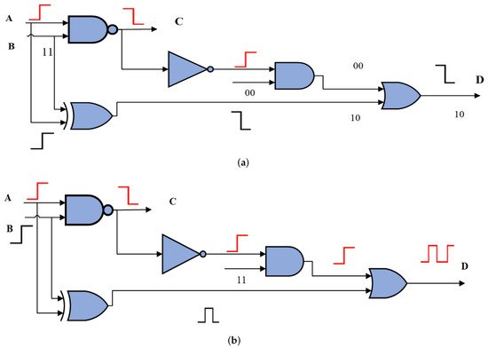
Figure 1. (a) TDF based pattern generation to propagate the fault at node A; (b) PDF based pattern generation for the path A to D.
2.1. Advantage of LOC over LOS
The major difference between LOC and LOS lies in the launch of transition. In LOC, the transition is launched at the at-speed functional launch clock cycle, but in LOS, the transition is launched at the last shift cycle. The LOS scheme is difficult to implement for high operating frequency because of the complexity of generating a high-speed switching scan enable (SE) signal. Figure 2a illustrates the waveform of the LOC scheme for pattern generation. Here the SE signal is de-asserted before the launch clock edge. Hence avoiding the need for high-speed switching SE signal. Figure 2b illustrates the waveform for the LOS scheme. Here the clock for launching the transition is in shift mode, and the SE signal has to be switched between the launch and capture clock cycle, which demands a high-speed SE signal.
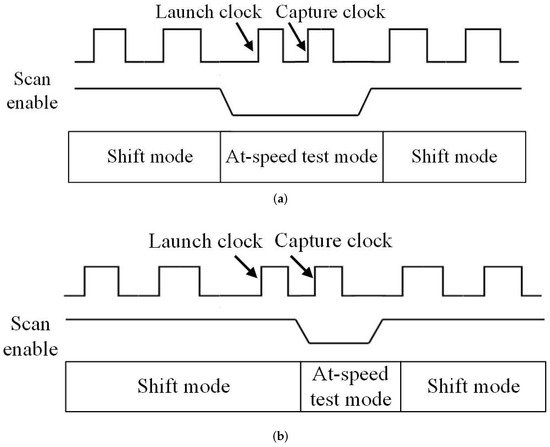
Figure 2. (a) Waveform for LOC based scheme for pattern generation; (b) Waveform for LOS based scheme for pattern generation.
Figure 3 and Figure 4 shows the result comparison of LOS and LOC based test pattern generation scheme for delay faults that evolved over time [14]. Figure 3 compares the test coverage of both the schemes produced by the commercial ATPG tool. It can be inferred that the LOC scheme has evolved over time and provides better test coverage. Figure 4 represents the pattern count for both the schemes generated by the commercial ATPG tool over the years. By comparing both Figure 3 and Figure 4. It can be inferred that the test coverage of LOC has been improving at the expense of pattern count. As compared to 2006, the test coverage of LOC has improved and is very close to that of LOS in 2012. But the pattern count is more. In 2019 noticeable test coverage increase is found in the case of LOC than in LOS, but still, the pattern count is higher. This is the case when the test coverage of LOC is more than the LOS. But in [14], it is reported that the pattern count will be almost equal for the same test coverage in the year 2019. This shows that the LOC scheme has been evolving in commercial tools in terms of test coverage. But in the case of run time, the LOS scheme remains better. Still, the LOC scheme-based pattern generation can be adopted, especially for low-cost testers.
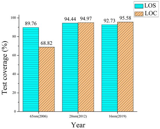
Figure 3. Result comparison of LOC and LOS based test coverage (commercial ATPG tool) with the evolution of years [14].
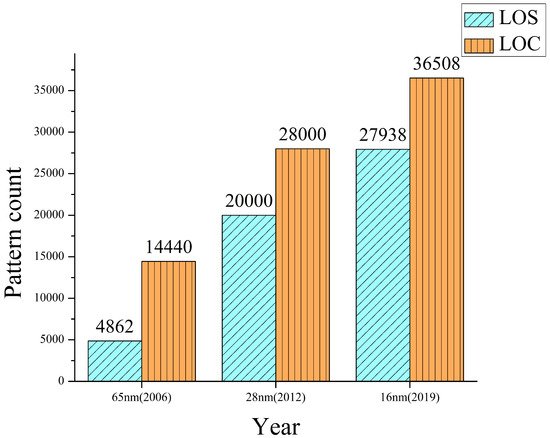
Figure 4. Comparison of LOS and LOC based pattern count (commercial ATPG tool) with the evolution of years [14].
3. Small Delay Defects vs. Hidden Delay Defects
3.1. Small Delay Defects
A small delay defect [15][16] is a type of delay defect that makes the chip fail during at-speed operation. The total path delay may go beyond the clock period when the small delays get propagated through the long paths. These delay defects will be huge enough to fail the circuit during the at-speed operation, but it will escape the traditional TDF model-based tests. The TDF model assumes that only large delay defects are localized in a single node, so whatever transition passes through this node will get delayed past the clock period. Hence, the TDF-based ATPG tool will try to propagate the fault effect through the easiest and shortest path possible to reduce the run time, as shown in Figure 5a. Here Path 1 and Path 2 are short paths through which the fault can be propagated, but the longest path is the third path mentioned as the Longest path in Figure 5a. If the TDF ATPG tool tries to propagate the fault effect through Path 1 or Path 2, then this will leave the small delay fault undetected. But this delay can cause the circuit to fail during at-speed functional operation.

Figure 5. (a) Delay of each path of the circuit through fault site X and the observation time T1 and T2 for detecting the small delay; (b) Delay of the path through the fault site X and the observation time T1 to detect the hidden delay.
3.2. Hidden Delay Defects
An HDD is a special type of SDD that does not fail the circuit during at-speed operations. These defects exist only in the shorter path. Even though the TDF model-based test generation propagates the fault effect through the short paths, the impact of fault is not visible at the particular at-speed operating frequency. This is clearly illustrated in Figure 5b. Assume that the longest path and the path sensitized by the pattern are the same. But the small delay effect is not visible during the at-speed clock period. These delay defects may grow due to aging effects and may cause early life failure and reliability issues [17].
References
- Moore, G.E. Cramming more components onto integrated circuits, Reprinted from Electronics, volume 38, number 8, April 19, 1965, pp.114 ff. IEEE Solid State Circuits Soc. Newsl. 2006, 11, 33–35.
- Brain, R. Interconnect scaling: Challenges and opportunities. In Proceedings of the 2016 IEEE International Electron Devices Meeting (IEDM), San Francisco, CA, USA, 3–7 December 2016; pp. 9.3.1–9.3.4.
- Piplani, S.; Visweswaran, G.S.; Kumar, A. Impact of crosstalk and process variation on capture power reduction for at-speed test. In Proceedings of the 2016 IEEE 34th VLSI Test Symposium (VTS), Las Vegas, NV, USA, 25–27 April 2016; pp. 1–6.
- Faisal, W.; Knotter, D.M.; Mud, A.; Kupera, F.G. Impact of particles in ultra pure water on random yield loss in IC production. Microelectron. Eng. 2009, 86, 140–144.
- Montanes, R.; de Gyvez, J.; Volf, P. Resistance characterization for weak open defects. IEEE Des. Test Comput. 2002, 19, 18–26.
- Zisser, W.H.; Ceric, H.; Weinbub, J.; Selberherr, S. Electromigration induced resistance increase in open TSVs. In Proceedings of the 2014 International Conference on Simulation of Semiconductor Processes and Devices (SISPAD), Yokohama, Japan, 23 October 2014; pp. 249–252.
- Ghaida, R.S.; Zarkesh-Ha, P. A Layout Sensitivity Model for Estimating Electromigration-Vulnerable Narrow Interconnects. J. Electron. Test. 2009, 25, 67–77.
- Villacorta, H.; Champac, V.; Gomez, R.; Hawkins, C.; Segura, J. Reliability Analysis of Small-Delay Defects Due to Via Narrowing in Signal Paths. IEEE Des. Test 2013, 30, 70–79.
- Waicukauski, J.A.; Lindbloom, E.; Rosen, B.K.; Iyengar, V.S. Transition Fault Simulation. IEEE Des. Test Comput. 1987, 4, 32–38.
- Pomeranz, I. A Metric for Identifying Detectable Path Delay Faults. IEEE Trans. Comput. Aided Des. Integr. Circuits Syst. 2012, 31, 1734–1742.
- Majhi, A.; Agrawal, V. Delay fault models and coverage. In Proceedings of the Eleventh International Conference on VLSI Design, Chennai, India, 4–7 January 1998; pp. 364–369.
- Savir, J.; Patil, S. On broad-side delay test. IEEE Trans. Very Large Scale Integr. VLSI Syst. 1994, 2, 368–372.
- Savir, J.; Patil, S. Scan-based transition test. IEEE Trans. Comput. Aided Des. Integr. Circuits Syst. 1993, 12, 1232–1241.
- Pandey, K. A Critical Engineering Dissection of LOS and LOC At-speed Test Approaches. In Proceedings of the 2020 IEEE International Test Conference India, Bangalore, India, 12–14 July 2020; pp. 1–7.
- Ahmed, N.; Tehranipoor, M.; Jayaram, V. Timing-based delay test for screening small delay defects. In Proceedings of the 2006 43rd ACM/IEEE Design Automation Conference, San Francisco, CA, USA, 24–28 July 2006; pp. 320–325.
- Sato, Y.; Hamada, S.; Maeda, T.; Takatori, A.; Nozuyama, Y.; Kajihara, S. Invisible delay quality-SDQM model lights up what could not be seen. In Proceedings of the IEEE International Conference on Test, Austin, TX, USA, 8 November 2005; pp. 9–1210.
- Qian, X.; Singh, A.D. Distinguishing Resistive Small Delay Defects from Random Parameter Variations. In Proceedings of the 2010 19th IEEE Asian Test Symposium, Shanghai, China, 1–4 December 2010; pp. 325–330.
More
Information
Subjects:
Engineering, Electrical & Electronic
Contributors
MDPI registered users' name will be linked to their SciProfiles pages. To register with us, please refer to https://encyclopedia.pub/register
:
View Times:
2.1K
Revisions:
2 times
(View History)
Update Date:
30 Sep 2022
Table of Contents


Notice
You are not a member of the advisory board for this topic. If you want to update advisory board member profile, please contact office@encyclopedia.pub.
OK
Confirm
Only members of the Encyclopedia advisory board for this topic are allowed to note entries. Would you like to become an advisory board member of the Encyclopedia?
Yes
No
${ textCharacter }/${ maxCharacter }
Submit
Cancel
Back
Comments
${ item }
|
${ item.createdUser.fullName }
${ item.createdAt }
${ item.vote }
${ item.reply }
Delete
${ reply.createdUser.fullName }
${ reply.createdAt }
${ reply.vote }
Delete
There is no reply to this comment~
${ item.replyTextCharacter }/${ item.replyMaxCharacter }
Submit
Cancel
More
No more~
There is no comment~
${ textCharacter }/${ maxCharacter }
Submit
Cancel
${ selectedItem.replyTextCharacter }/${ selectedItem.replyMaxCharacter }
Submit
Cancel
Confirm
Are you sure to Delete?
Yes
No