Your browser does not fully support modern features. Please upgrade for a smoother experience.
Submitted Successfully!
 +1 credit
Thank you for your contribution! You can also upload a video entry or images related to this topic.
For video creation, please contact our Academic Video Service.
| Version | Summary | Created by | Modification | Content Size | Created at | Operation |
|---|---|---|---|---|---|---|
| 1 | Paweł Węgierek | -- | 4815 | 2022-08-24 18:39:57 | | | |
| 2 | Beatrix Zheng | + 2 word(s) | 4817 | 2022-08-25 08:16:57 | | | | |
| 3 | Beatrix Zheng | Meta information modification | 4817 | 2022-08-25 08:17:47 | | |
Video Upload Options
We provide professional Academic Video Service to translate complex research into visually appealing presentations. Would you like to try it?
Cite
If you have any further questions, please contact Encyclopedia Editorial Office.
Pastuszak, J.; Węgierek, P. Photovoltaic Cell Generations. Encyclopedia. Available online: https://encyclopedia.pub/entry/26456 (accessed on 30 July 2026).
Pastuszak J, Węgierek P. Photovoltaic Cell Generations. Encyclopedia. Available at: https://encyclopedia.pub/entry/26456. Accessed July 30, 2026.
Pastuszak, Justyna, Paweł Węgierek. "Photovoltaic Cell Generations" Encyclopedia, https://encyclopedia.pub/entry/26456 (accessed July 30, 2026).
Pastuszak, J., & Węgierek, P. (2022, August 24). Photovoltaic Cell Generations. In Encyclopedia. https://encyclopedia.pub/entry/26456
Pastuszak, Justyna and Paweł Węgierek. "Photovoltaic Cell Generations." Encyclopedia. Web. 24 August, 2022.
Copy Citation
Solar energy is one of the most demanding renewable sources of electricity. Electricity production using photovoltaic technology not only helps meet the growing demand for energy, but also contributes to mitigating global climate change by reducing dependence on fossil fuels. The level of competitiveness of innovative next-generation solar cells is increasing due to the efforts of researchers and scientists related to the development of new materials, particularly nanomaterials and nanotechnology.
photovoltaic
solar cells
renewable energy
photovoltaic cell manufacturing technologies
efficiency
photovoltaic generations
1. Introduction
In the past decade, photovoltaics have become a major contributor to the ongoing energy transition. Advances relating to materials and manufacturing methods have had a significant role behind that development. However, there are still numerous challenges before photovoltaics can provide cleaner and low-cost energy. Research in this direction is focused on efficient photovoltaic devices such as multi-junction cells, graphene or intermediate band gap cells, and printable solar cell materials such as quantum dots [1].
The primary role of a photovoltaic cell is to receive solar radiation as pure light and transform it into electrical energy in a conversion process called the photovoltaic effect. There are several technologies involved with the manufacturing process of photovoltaic cells, using material modification with different photoelectric conversion efficiencies in the cell components. Due to the emergence of many non-conventional manufacturing methods for fabricating functioning solar cells, photovoltaic technologies can be divided into four major generations, which is shown in Figure 1 [2].
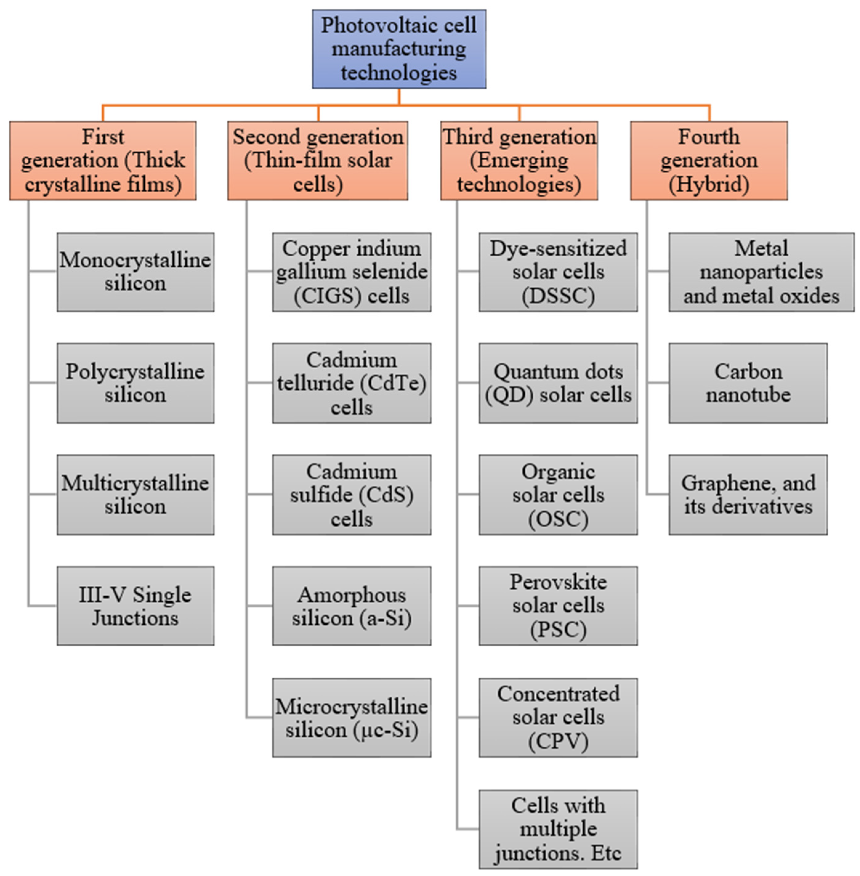
Figure 1. Various solar cell types and current developments within this field [3].
The generations of various photovoltaic cells essentially tell the story of the stages of their past evolution. There are four main categories that are described as the generations of photovoltaic technology for the last few decades, since the invention of solar cells [4]:
-
First Generation: This category includes photovoltaic cell technologies based on monocrystalline and polycrystalline silicon and gallium arsenide (GaAs).
-
Second Generation: This generation includes the development of first-generation photovoltaic cell technology, as well as the development of thin film photovoltaic cell technology from “microcrystalline silicon (µc-Si) and amorphous silicon (a-Si), copper indium gallium selenide (CIGS) and cadmium telluride/cadmium sulfide (CdTe/CdS) photovoltaic cells”.
-
Third Generation: This generation counts photovoltaic technologies that are based on more recent chemical compounds. In addition, technologies using nanocrystalline “films,” quantum dots, dye-sensitized solar cells, solar cells based on organic polymers, etc., also belong to this generation.
-
Fourth Generation: This generation includes the low flexibility or low cost of thin film polymers along with the durability of “innovative inorganic nanostructures such as metal oxides and metal nanoparticles or organic-based nanomaterials such as graphene, carbon nanotubes and graphene derivatives” [4].
Examples of solar cell types for each generation along with average efficiencies are shown in Figure 2.
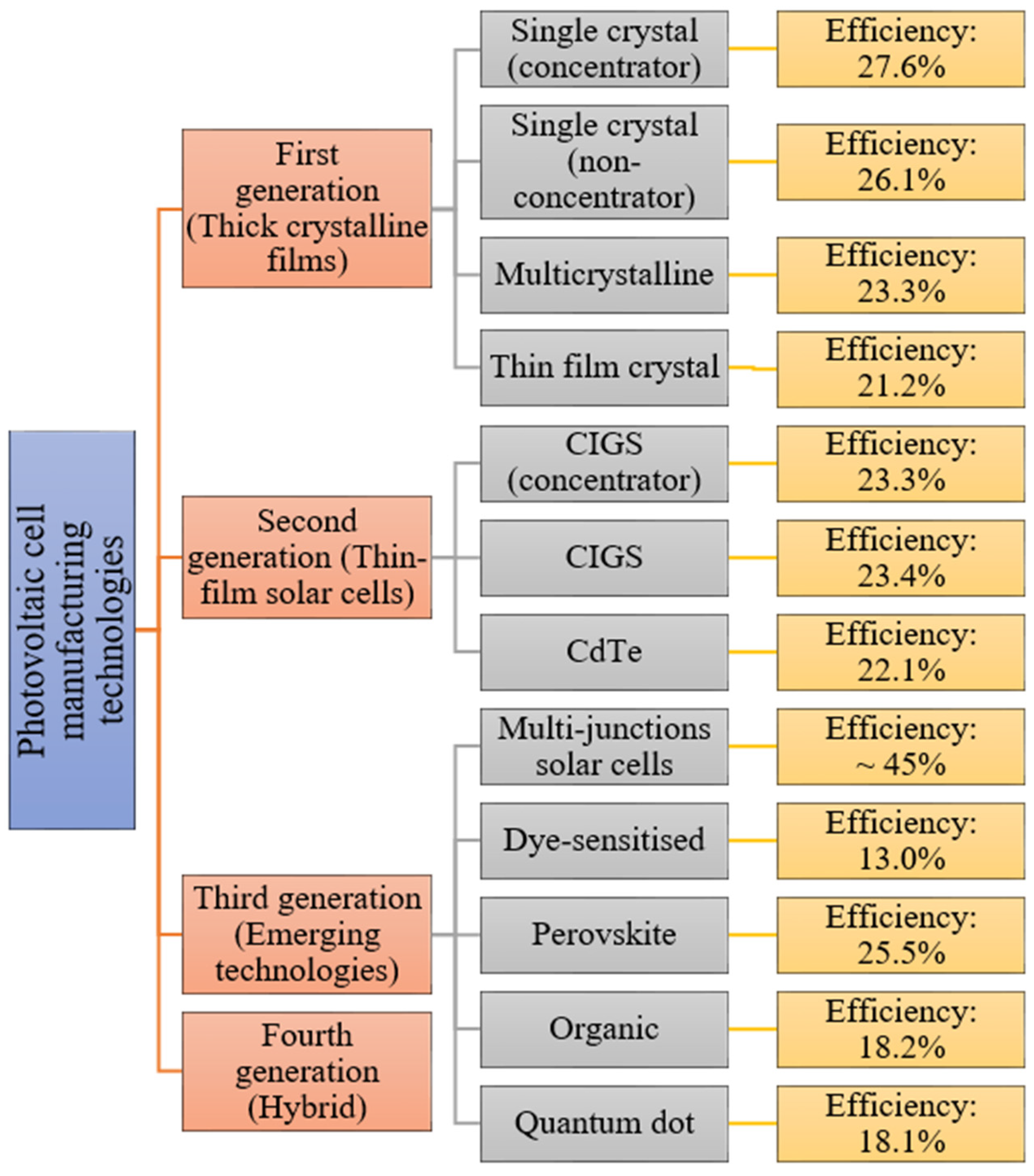
Figure 2. Examples of photovoltaic cell efficiencies [5].
2. First Generation of Photovoltaic Cells
Silicon-based PV cells were the first sector of photovoltaics to enter the market, using processing information and raw materials supplied by the industry of microelectronics. Solar cells based on silicon now comprise more than 80% of the world’s installed capacity and have a 90% market share. Due to their relatively high efficiency, they are the most commonly used cells. The first generation of photovoltaic cells includes materials based on thick crystalline layers composed of Si silicon. This generation is based on mono-, poly-, and multicrystalline silicon, as well as single III-V junctions (GaAs) [6][7].
Comparison of first-generation photovoltaic cells [7]:
-
Solar cells based on monocrystalline silicon (m-si)
Efficiency: 15 ÷ 24%; Band gap: ~1.1 eV; Life span: 25 years; Advantages: Stability, high performance, long service life; Restrictions: High manufacturing cost, more temperature sensitivity, absorption problem, material loss.
-
Solar cells based on polycrystalline silicon (p-si)
Efficiency: 10 ÷ 18%; Band gap: ~1.7 eV; Life span: 14 years; Advantages: Manufacturing procedure is simple, profitable, decreases the waste of silicon, higher absorption compared to m-si; Restrictions: Lower efficiency, higher temperature sensitivity.
-
Solar cells based on GaAs
Efficiency: 28 ÷ 30%; Band gap: ~1.43 eV; Life span: 18 years; Advantages: High stability, lower temperature sensitivity, better absorption than m-si, high efficiency; Restrictions: Extremely expensive [7].
The first generation concerns p-n junction-based photovoltaic cells, which are mainly represented by mono- or polycrystalline wafer-based silicon photovoltaic cells. Monocrystalline silicon solar cells involve growing Si blocks from small monocrystalline silicon seeds and then cutting them to form monocrystalline silicon wafers, which are fabricated using the Czochralski process (Figure 3a). Monocrystalline material is widely used due to its high efficiency compared to multicrystalline material. Key technological challenges associated with monocrystalline silicon include stringent requirements for material purity, high material consumption during cell production, cell manufacturing processes, and limited module sizes composed of these cells [8].
Multicrystalline silicon blocks are produced through melting high-purity silicon and crystallizing it in a big crucible by directional solidification process (Figure 3b). There is no reference crystal orientation in this process, as in the Czochralski process, and therefore, silicon material with different orientations is produced. The most commonly used base material for solar cells are p-type Si substrates doped with boron. The n-type silicon substrates are also used for the fabrication of high-efficiency solar cells, but they present additional technical challenges, such as achieving uniform doping along the silicon block in comparison to p-type substrates [9].
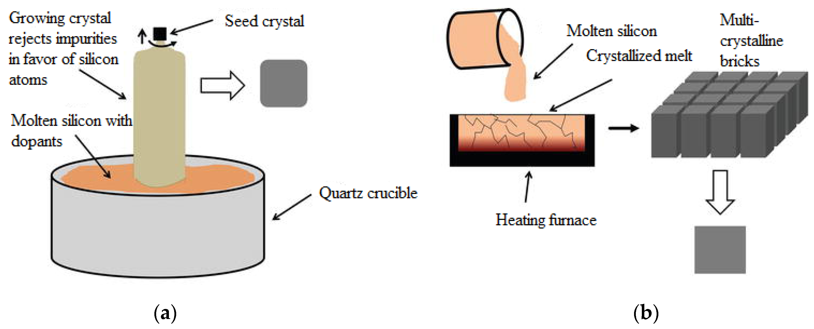
Figure 3. A picture showing (a) the Czochralski process for monocrystalline blocks and (b) the process of directional solidification for multicrystalline blocks [10].
In the production of crystalline solar cells, six or more steps need to be carried out sequentially. These typically include surface texturing, doping, diffusion, oxide removal, anti-reflective coating, metallization, and firing. At the end of the process, the cell efficiency and other parameters are measured (under standard test conditions). The efficiency of photovoltaic cells is determined by the material quality that is used in their manufacture [10].
The theoretical efficiency threshold for first-generation PV cells appears to have been estimated at 29.4%, and a sufficiently close value was reached as early as two decades ago. At the laboratory scale, reaching 25% efficiency was recorded as early as 1999, and since then, very minimal improvements in efficiency values have been achieved. Since the appearance of crystalline silicon photovoltaic cells, their efficiency has increased by 20.1%, from 6% when they were first discovered to the current record of 26.1% efficiency. There are factors that limit cell efficiency, such as volume defects. Breakthroughs in the production of these cells include the introduction of an aluminum back surface field (Al-BSF) to reduce the recombination rate on the back surface, or the development of Passivated Emitter and Rear Cell (PERC) technology to further reduce the recombination rate on the back surface [11]
3. Second Generation of Photovoltaic Cells
The thin film photovoltaic cells based on CdTe, gallium selenide, and copper (CIGS) or amorphous silicon have been designed to be a lower-cost replacement for crystalline silicon cells. They offer improved mechanical properties that are ideal for flexible applications, but this comes with the risk of reduced efficiency. Whereas the first generation of solar cells was an example of microelectronics, the evolution of thin films required new methods of growing and opened the sector up to other areas, including electrochemistry [12].
The second-generation photovoltaic cell comparison [7]:
-
Solar cells based on amorphous silicon (a-si)
Efficiency: 5 ÷ 12%; Band gap: ~1.7 eV; Life span: 15 years; Advantages: Less expensive, available in large quantities, non-toxic, high absorption coefficient; Restrictions: Lower efficiency, difficulty in selecting dopant materials, poor minority carrier lifetime.
-
Solar cells based on cadium telluride/cadium sulfide (CdTe/CdS)
Efficiency: 15 ÷ 16%; Band gap: ~1.45 eV; Life span: 20 years; Advantages: High absorption rate, less material required for production; Restrictions: Lower efficiency, Cd being extremely toxic, Te being limited, more temperature-sensitive.
-
Solar cells based on copper indium gallium selenide (CIGS)
Efficiency: 20%; Band gap: ~1.7 eV; Life span: 12 years; Advantages: Less material required for production; Restrictions: Very high-priced, not stable, more temperature-sensitive, highly unreliable [7].
4. Third Generation of Photovoltaic Cells
The third generation of solar cells (including tandem, perovskite, dye-sensitized, organic, and emerging concepts) represent a wide range of approaches, from inexpensive low-efficiency systems (dye-sensitized, organic solar cells) to expensive high-efficiency systems (III-V multi-junction cells) for applications that range from building integration to space applications. Third-generation photovoltaic cells are sometimes referred to as “emerging concepts” because of their poor market penetration, even though some of these have been studied for more than 25 years [13].
The latest trends in silicon photovoltaic cell development are methods involving the generation of additional levels of energy in the semiconductor’s band structure. The most advanced studies of manufacturing technology and efficiency improvements are now concentrated on third-generation solar cells.
One of the current methods to increase the efficiency of PV cells is the introduction of additional energy levels in the semiconductor’s band gap (IBSC and IPV cells) and the increasing use of ion implantation in the manufacturing process. Other innovative third-generation cells that are lesser-known commercial “emerging” technologies include [14]:
-
Organic materials (OSC) photovoltaic cells;
-
Perovskites (PSC) photovoltaic cells;
-
Dye-sensitized (DSSC) photovoltaic cells;
-
Quantum dots (QD) photovoltaic cells; and
-
Multi-junction photovoltaic cells [14].
Third-generation photovoltaic cell comparison [7]:
-
Solar cells based on dye-sensitized photovoltaic cells
Efficiency: 5 ÷ 20%; Advantages: Lower cost, low light and wider angle operation, lower internal temperature operation, robustness, and extended lifetime; Restrictions: Problems with temperature stability, poisonous and volatile substances.
-
Solar cells based on quantum dots
Efficiency: 11 ÷ 17%; Advantages: Low production cost, low energy consumption; Restrictions: High toxicity in nature, degradation.
-
Solar cells based on organic and polymeric photovoltaic cells
Efficiency: 9 ÷ 11%; Advantages: Low processing cost, lighter weight, flexibility, thermal stability; Restrictions: Low efficiency.
-
Solar cells based on perovskite
Efficiency: 21%; Advantages: Low-cost and simplified structure, light weight, flexibility, high efficiency, low manufacturing cost; Restrictions: Unstable.
-
Multi-junction solar cells
4.1. Organic and Polymeric Materials Photovoltaic Cells (OSC)
Organic solar cells (OSCs) are beneficial in applications related to solar energy since they have the potential to be used in a variety of prospects on the basis of the unique benefits of organic semiconductors, including their ability to be processed in solution, light weight, low cost, flexibility, semi-transparency, and applicability to large-scale roll-to-roll processing. Solution-processed organic solar cells (OSCs) that absorb near-infrared (NIR) radiation have been studied worldwide for their potential to be donor:acceptor bulk heterojunction (BHJ) compounds. In addition, NIR-absorbing OSCs have attracted attention as high-end equipment in next-generation optoelectronic devices, such as translucent solar cells and NIR photodetectors, because of their potential for industrial applications. With the introduction of non-fullerene acceptors (NFAs) that absorb light in the NIR range, the value of OSC is increasing, while organic donor materials capable of absorbing light in the NIR range have not yet been actively studied compared to acceptor materials that absorb light in the NIR range [15].
The most advanced BHJ structure by combining organic donor and acceptor materials showed tremendous hope for low-cost and lightweight organic solar cells. Over the past decade, enormous progress was made, with power conversion efficiencies reaching more than 14% for a single-junction device and more than 17% for a tandem device through the design of new NIR photoactive materials with low bandwidth. Compared to wide-band organic photovoltaic materials, low-band donor and non-fullerene acceptor materials with wide-range solar coverage extended to the NIR region typically exhibit more tightly superimposed electronic orbitals, easier delocalization of π electrons, higher dielectric constant, stronger dipole moment, and lower exciton binding energy. These properties make low-bandwidth photovoltaic materials play an important role in high-performance organic solar cells, including single-junction and tandem devices [16].
A clever strategy in active layer design could be summed up as optimizing the weight ratio of donor to acceptor materials, using ultra-low band gap materials as a third component to improve NIR light utilization efficiency, and adjusting the thickness of the active layer to achieve a compromise between photon collection and charge accumulation. Much effort has gone into optimizing the translucent top electrode: well-balanced conductivity and transmittance in the visible light range, increased reflectance in the NIR or ultraviolet (UV) light range, and better compatibility with active layers. In terms of device engineering, photon crystal, anti-reflection coating, optical microcavity, and dielectric/metal/dielectric (DMD) structures have been placed to realize selective transmission and reflection for simultaneous improvement of power conversion efficiency and average transmission of translucent OSC visible light [17].
4.2. Dye-Sensitized Photovoltaic Cells (DSSC)
Conjugated polymers and organic semiconductors have been successful in flat panel displays and LEDs, so they are considered advanced materials in the current generation of photovoltaic cells. A schematic representation of dye-sensitized organic photovoltaic cells (DSSCs) is shown in Figure 4. Polymer/organic photovoltaic cells can also be divided into dye-sensitized organic photovoltaic cells (DSSCs), photoelectrochemical photovoltaic cells, and plastic (polymer) and organic photovoltaic devices (OPVDs), differing in mechanism of operation [18].
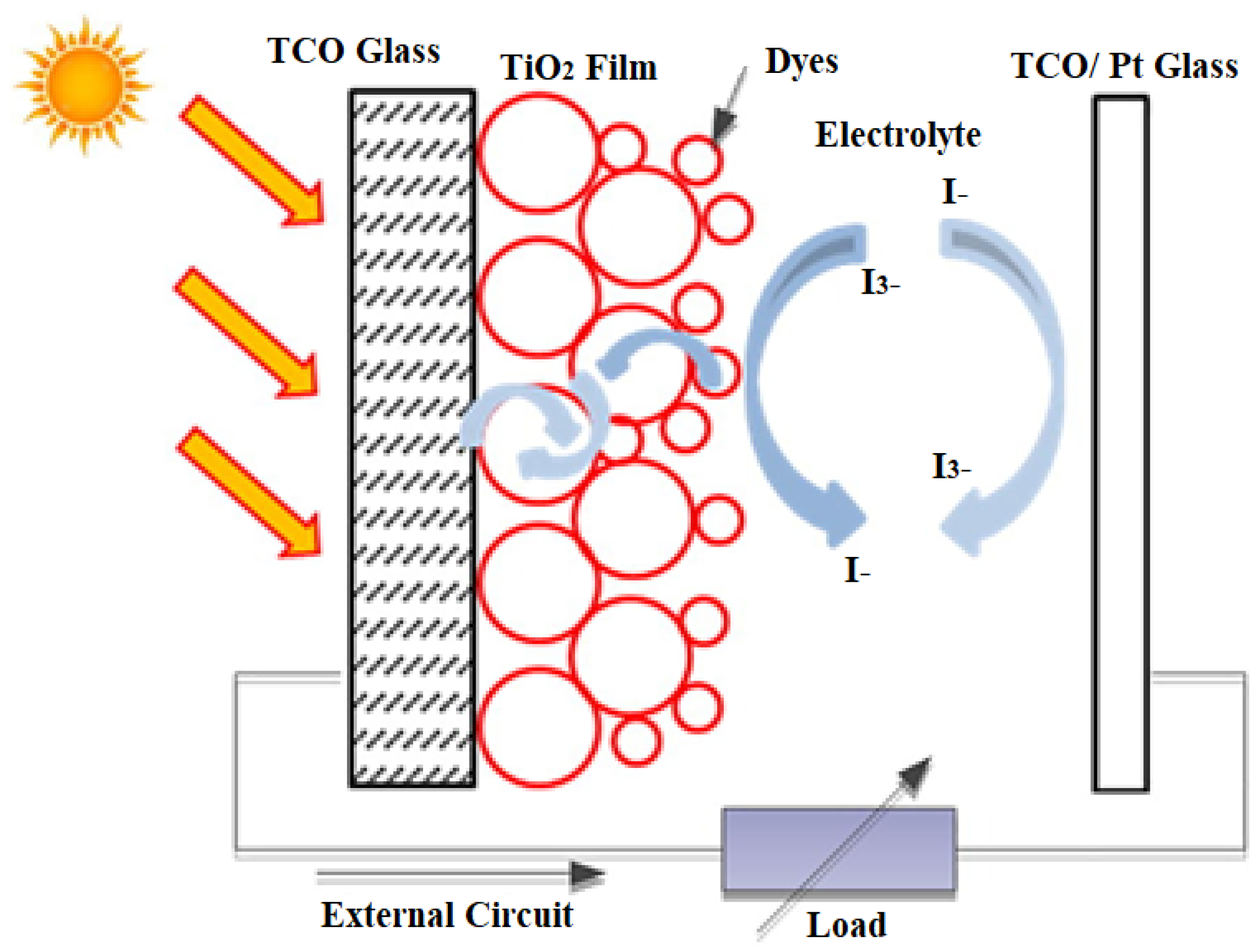
Figure 4. Schematic representation of a DSSCs [19].
Dye-sensitized solar cells (DSSCs) represent one of the best nanotechnology materials for energy harvesting in photovoltaic technologies. It is a hybrid organic–inorganic structure where a highly porous, nanocrystalline layer of titanium dioxide (TiO2) is used as a conductor of electrons in contact with an electrolyte solution also containing organic dyes that absorb light near the interfaces. A charge transfer occurs at the interface, resulting in the transport of holes in the electrolyte. The power conversion efficiency has been shown to be about 11%, and commercialization of dye-sensitized photovoltaic modules is underway. A novel feature in DSSC solar cells is the photosensitization of nanosized TiO2 coatings in combination with optically active dyes, which increases their efficiency to more than 10% [20].
DSSCs hold promise as photovoltaic devices because of their simple fabrication, low material costs, and their benefits in transparence, color capability, and mechanical flexibility. The main challenges in commercializing DSSCs are poor photoelectric conversion efficiency and cell stability. The highest attainable theoretical energy conversion efficiency was estimated at 32% for DSSCs; however, the highest efficiency reported to date is only 13%. Intensive work is underway to understand the parameters governing the DSSC to improve its efficiency. Numerous attempts have been made to optimize the redox pair and absorbance of the dye, modify a wide band gap semiconductor as a working electrode, and develop a counter electrode (CE). In addition to increasing the efficiency of DSSC, the cost of materials is another major issue that needs to be solved in future work [21].
4.3. Perovskite Photovoltaic Cells
Perovskite solar cells (PSCs) are a revolutionary new photovoltaic cell concept that relies on metal halide perovskites (MHPs), e.g., methylammonium iodide as well as formamidine lead iodide (MAPbI3 or FAPbI3, respectively). MHPs integrate a number of features favored in photovoltaic absorbers, including a direct band gap with a high absorption coefficient, long carrier lifetime and diffusion length, low defect density, and ease of tuning the composition and band gap. In the year 2009, MHP was first described as a sensitizer in a dye cell based on liquid electrolyte conducting holes. In 2012, MHP demonstrating ~10% efficiency of PSCs based on a solid-state hole conductor sparked an explosion of PSC studies. In about a decade of research, the efficiency of a single PSC junction increased to a certified level of 25.2% [22].
The development of PSCs has been heavily influenced by the improvement of material quality through a broad range of synthetic methods designed under the guidance of a fundamental understanding of MHP growth mechanisms. Comprehension of the complex and correlated processes of perovskite growth (e.g., nucleation, grain growth, as well as microstructure evolution) has aided in the development of a broad range of high-efficiency growth modes (for example, single-step growth, sequential growth, dissolution process, vapor process, post-deposition processing, non-stoichiometric growth, additive-assisted growth, and fine-tuning of structure dimensions). The latest efforts were concentrated on interface engineering, focusing on reducing open-circuit voltage losses and improving stability, particularly by introducing a two-dimensional perovskite surface layer. With progress in synthetic control, the perovskite composition is becoming simpler, mainly toward FAPbI3. This will undoubtedly contribute to the simplification of scale deposition methods and a basic understanding of the properties of these cells [23].
4.4. Quantum Dots Photovoltaic Cells
Solar cells made from these materials are called quantum dots (QDs) and are also known as nanocrystalline solar cells. They are fabricated by epitaxial growth on a substrate crystal. Quantum dots are surrounded by high potential barriers in a three-dimensional shape, and the electrons and electron holes in a quantum dot become discrete energy because they are confined in a small space (Figure 5). Consequently, the ground state energy of electrons and electron holes in a quantum dot depends on the size of the quantum dot [24].
Nanocrystalline cells have relatively high absorption coefficients. Four consecutive processes occur in a solar cell: (1) light absorption and exciton formation, (2) exciton diffusion, (3) charge separation, and (4) charge transport. Due to the poor mobility and short lifetime of excitons in conducting polymers, organic compounds are characterized by small exciton diffusion lengths (10–20 nm). In other words, excitons that form far from the electrode or carrier transport layer recombine and the conversion efficiency drops [25].
The development of thin film solar cells with metal halide perovskites has led to intensive attention to the corresponding nanocrystals (NCs) or quantum dots (QDs). Today, the record efficiency of QD solar cells was improved to 16.6% using mixed colloidal QDs with perovskites. The universality of these new nanomaterials regarding ease of fabrication and the ability to tune the band gap and control the surface chemistry allows a variety of possibilities for photovoltaics, such as single-junction, elastic, translucent, controlled cells with heterostructures and multi-junction tandem solar cells which would push the field even further. However, a narrower size distribution has the potential to enhance the performance of QD solar cells through more ways than one. Firstly, electron transport might be better in smaller QDs, as larger QDs function as a band tail or shallow trap that makes transport more difficult. Secondly, the open-circuit voltage (VOC) of QD solar cells could be limited by the smallest band gap (largest size) QD near the contacts. Enhancing the homogeneity and uniformity of QD size would also improve PV performance by the minimization of such losses. Although controlled experiments such as these have not yet been reported, it is possible that more controlled synthesis might provide benefits to QD cells [26].
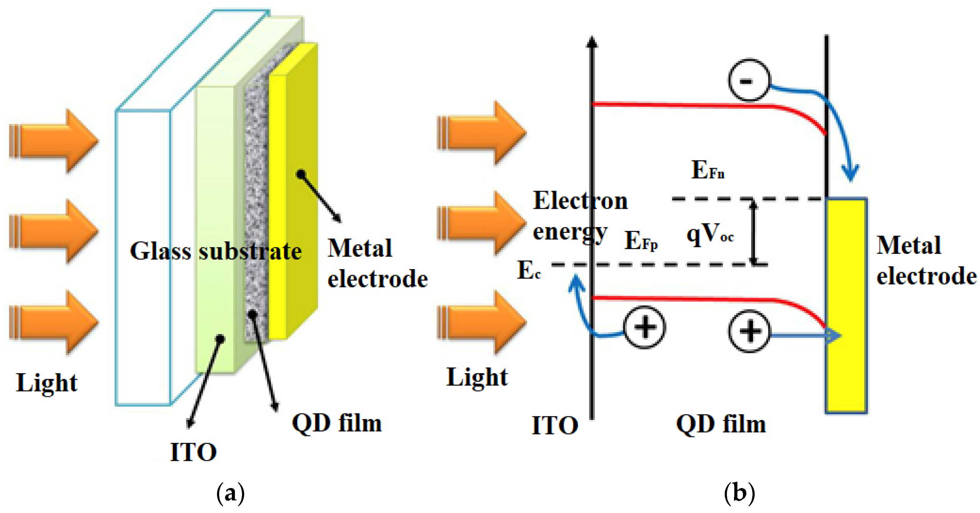
Figure 5. (a) A scheme of a solar cell based on quantum dots, (b) solar cell band diagram [27].
4.5. Multi-Junction Photovoltaic Cells
Multi-junction (MJ) solar cells consist of plural p-n junctions fabricated from various semiconductor materials, with each junction producing an electric current in response to light of a different wavelength, thereby improving the conversion of incident sunlight into electricity and the efficiency of the device. The concept to use various materials with different band gaps has been suggested to utilize the maximum possible number of photons and is known as a tandem solar cell. An entire cell could be fabricated from the same or different materials, giving a broad spectrum of possible designs [28].
Usually, the cells are integrated monolithically and connected in series through a tunnel junction, and current matching between cells is obtained through adjusting each cell’s band gap and thickness. The theoretical feasibility of using multiple band gaps was examined and was found to be 44% for two band gaps, 49% for three band gaps, 54% for four band gaps, and 66% for an infinite number of gaps. Figure 6 illustrates a scheme of an InGaP/(In)GaAs/Ge triple solar cell and presents crucial technologies to enhance efficiency of conversion [29].
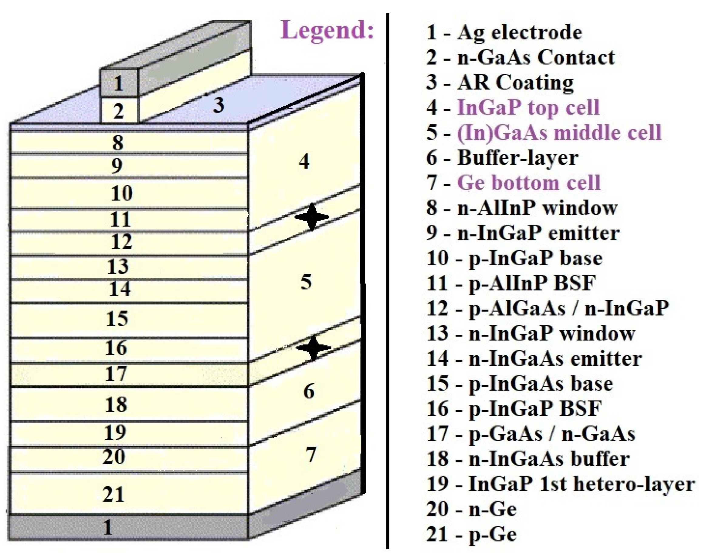
Figure 6. Schematic illustration of a triple-junction cell and approaches for improving efficiency of the cell [28].
Grid-matched InGaP/(In)GaAs/Ge triple solar cells have been widely used in space photovoltaics and have achieved the highest true efficiency of over 36%. Heavy radiation bombardment of various energetic particles in the space environment inevitably damages solar cells and causes the formation of additional non-radiative recombination centers, which reduces the diffusion length of minority carriers and leads to a reduction in solar cell efficiency. The sub-cells in multi-junction solar cells are connected in series; the sub-cell with the greatest radiation degradation degrades the efficiency of the multi-junction solar cell. To improve the radiation resistance of (In)GaAs sub-cells, measures such as reducing the dopant concentration, decreasing the thickness of the base region, etc., can be used [29].
4.6. Photovoltaic Cells with Additional Intermediate Band
The National Renewable Energy Laboratory (NREL) estimates that multi-junction and IBSC photovoltaic cells have the highest efficiency under experimental conditions (47.1%). The main feature of these cells is precisely the additional intermediate band in the band gap of silicon. Currently, two types of these cells are specified in the world literature: IBSC (Intermediate Band Solar Cells) and IPV (Impurity Photovoltaic Effect) [30].
Impurity Photovoltaic Effect (IPV) is one of the solutions used to increase the infrared response of PV cells and thus increase the solar-to-electric energy conversion efficiency. The idea of the IPV effect is based on the introduction of deep radiation defects in the structure of the semiconductor crystal structure. These defects ensure a multi-step absorption mechanism for photons with energies below the band gap width. The addition of IPV dopants into silicon solar cell structure, under certain conditions, increases the spectral response, short circuit current density, and conversion efficiency [31].
A major direction of study with great potential for development is Intermediate Band Solar Cells (IBSCs). They represent a third-generation solar cell concept and involve not only silicon, but also other materials. The idea behind the intermediate band gap solar cell (IBSC) concept is to absorb photons with an energy corresponding to the sub-band width in the cell structure. These photons are absorbed by a semiconductor-like material that, in addition to the conduction and valence bands, has an intermediate band (IB) in the conventional semiconductor’s band gap (Figure 7). In IBSCs, the silicon layers are implanted with very high doses of metal ions to create an additional energy level [32].
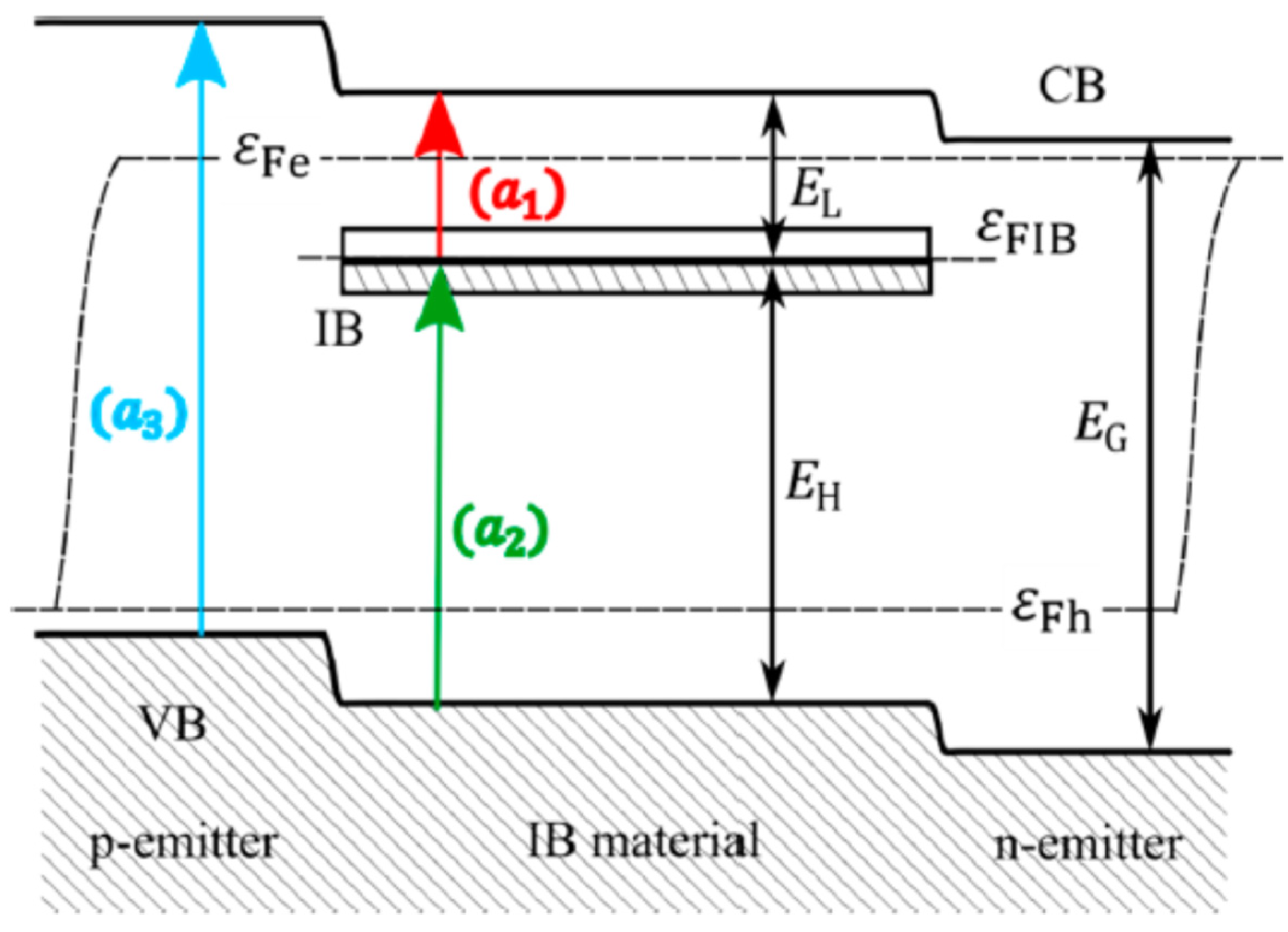
Figure 7. Energy band diagram of an intermediate band solar cell (IBSC) [32].
Based on the research conducted on the effect of defects introduced into the silicon structure, a model was developed according to which introducing selected deep defects into the charge carrier capture region results in improved PV cell efficiency. Of particular interest are defects that facilitate the transport of majority carriers and defects that counteract the accumulation of minority carriers. This contributes significantly to reducing the recombination process at the charge carrier capture site. Finally, by introducing defects into the structure of the silicon underlying the solar cell, the researchers combine effective surface passivation with simultaneous reduction in optical losses [33].
The introduction of intermediate bands in semiconductors, using ion implantation, can be executed using two methods: by introducing dopants of very high concentration into the semiconductor substrate, or by implanting the silicon layer with high-dose metal ions. The increasing use of ion implantation in the photovoltaic cell manufacturing process has the potential to reduce the cost of deployment and increase the cost-effectiveness of silicon cells by increasing their efficiency. The use of ion implantation technology provides increased precision of silicon layer doping and generation of additional levels of energy in the band gap, as well as shortening the individual stages of cell fabrication, which ultimately translates into improved quality and lower production costs [34].
Lately, the technique of ion implantation is gaining popularity in the solar industry, gradually displacing the diffusion technique that has been used for many years. As can be seen in Figure 8, cell performance is expected to continue to improve as the technology evolves toward higher efficiencies. In addition to local and reference doping, the major benefits of this technology involve high precision control of the amount and distribution of dopant doses, which results in high uniformity, repeatability, and increased efficiency (above 19%), with a significantly narrower distribution of cell performance [35].
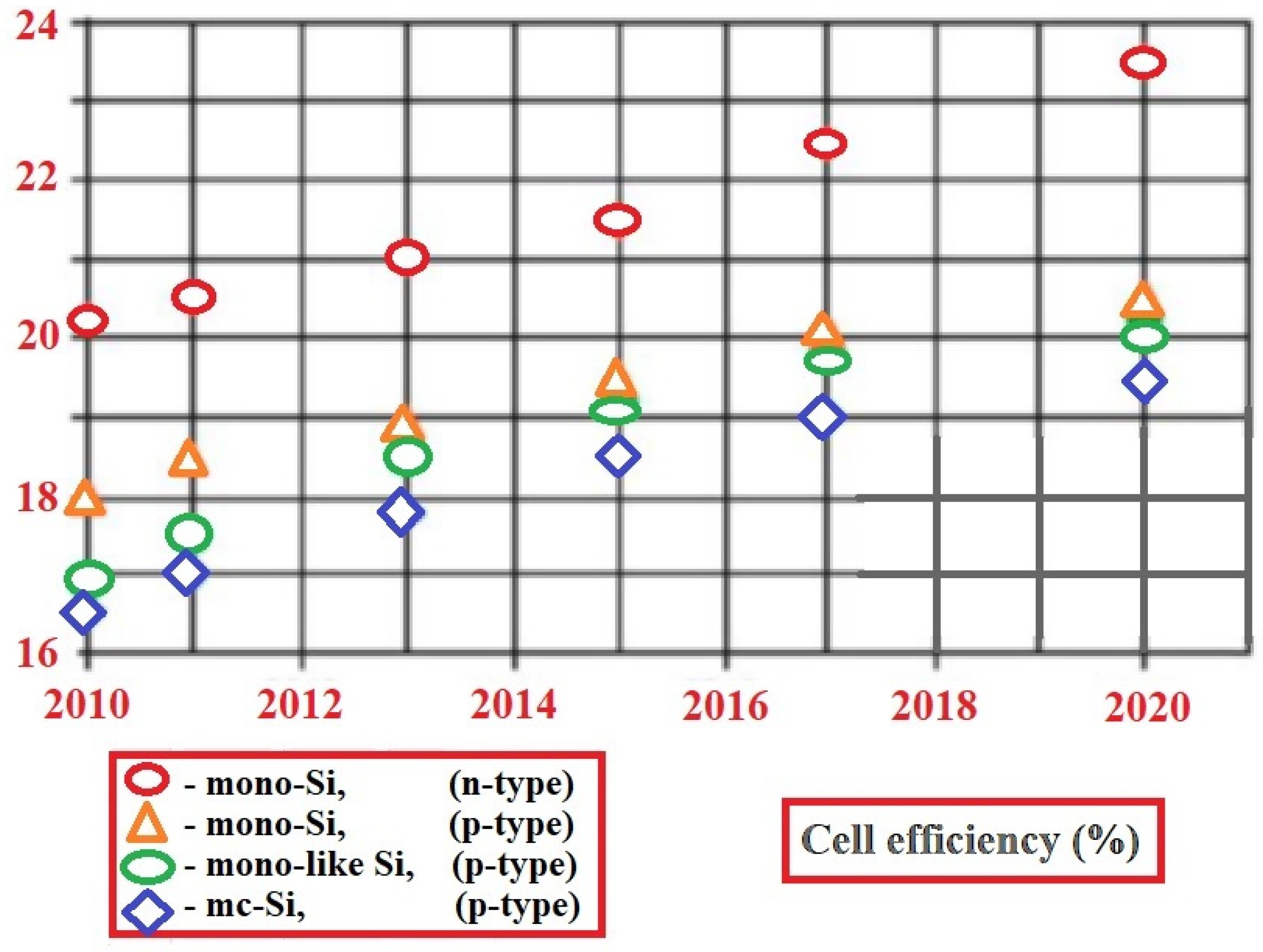
Figure 8. Stabilized cell efficiency trend curves [35].
In the method of ion implantation, chosen ions with the required impurity are inserted into the semiconductor by accelerating the impurity ions to a high energy level and implanting the ions into the semiconductor. The energy given to the impurity ions defines the depth of ion implantation. Contrary to the diffusion technology (where the impurity ion dose is introduced only at the surface), in the ion implantation technique, a controllable dose of impurity ions can be placed deeply into the semiconductor [36].
5. Fourth Generation of Photovoltaic Cells
Fourth-generation photovoltaic cells are also known as hybrid inorganic cells because they combine the low cost and flexibility of polymer thin films, with the stability of organic nanostructures such as metal nanoparticles and metal oxides, carbon nanotubes, graphene, and their derivatives. These devices, often referred to as “nanophotovoltaics”, could become the promising future of photovoltaics [37].
Graphene-Based Photovoltaic Cells
By using thin polymer layers and metal nanoparticles, as well as various metal oxides, carbon nanotubes, graphene, and their derivatives, the fourth generation provides excellent affordability and flexibility. Particular emphasis was placed on graphene because it is considered a nanomaterial of the future. Due to their unique properties, such as high carrier mobility, low resistivity and transmittance, and 2D lattice packing, graphene-based materials are being considered for use in PV devices instead of existing conventional materials. However, to achieve adequate device performance, the key to its practical applications is the synthesis of graphene materials with appropriate structure and properties [38].
Since the properties of graphene are fundamentally related to its fabrication process, a judicious choice of methods is essential for targeted applications. In particular, highly conductive graphene is suitable for use in flexible photovoltaic devices, and its high compatibility with metal oxides, metallic compounds, and conductive polymers makes it suitable for use as a selective charge-taking element and electrode interlayer material [39].
In the past two decades, graphene has been combined with the concept of photovoltaic material and is showing a significant role as a transparent electrode, hole/electron transport material, and interfacial buffer layer in solar cell devices. The researchers can distinguish several types of graphene-based solar cells, including organic bulk heterojunction (BHJ) cells, dye-sensitized cells, and perovskite cells. The energy conversion efficiency exceeded 20.3% for graphene-based perovskite solar cells and reached 10% for BHJ organic solar cells. In addition to its function of extracting and transporting charge to the electrodes, graphene plays another unique role—it protects the device from environmental degradation through its packed 2D lattice structure and ensures the long-term environmental stability of photovoltaic devices [40].
Semi-metallic graphene having a zero band gap creates Schottky junction solar cells with silicon semiconductors. Even though graphene was discovered for the first time in 2004, the first graphene–silicon solar cell was not characterized as an n-silicon cell until 2010. Figure 9 schematically shows a graphene–silicon solar cell with a Schottky junction. Graphene sheets (GS), cultured by chemical vapor deposition (CVD) on nickel films, were wet deposited on pre-patterned Si/SiO2 substrates with an effective area of 0.1–0.5 cm2. The graphene sheet forms a coating on the exposed n-Si substrate, creating a Schottky junction. The graphene sheet was contacted using Au electrodes [41].
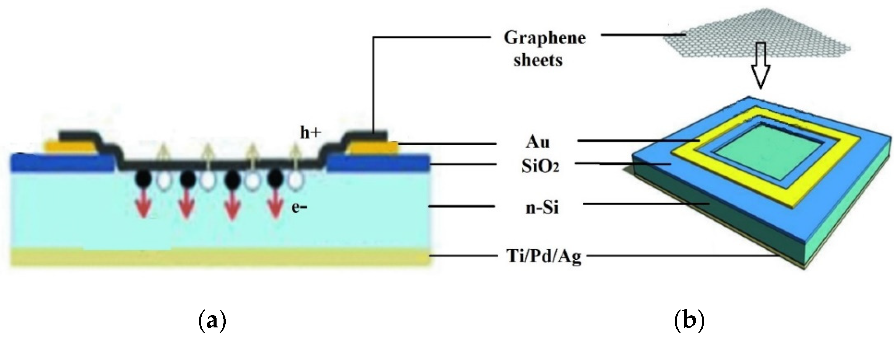
Figure 9. Graphene–silicon Schottky junction solar cell. (a) Cross-sectional view, (b) schematic illustration of the device configuration [38].
Graphene synthesis uses mainly two methodologies, which are the bottom-up and top-down methods. In the top-down approach, graphite is the starting material, and the goal is to intercalate and exfoliate it into graphene sheets by solid, liquid, or electrochemical exfoliation. Another approach under this categorization is the exfoliation of graphite oxide into graphene oxide (GO), after which chemical or thermal reduction takes place. A bottom-up approach is to produce graphene from molecular precursors by chemical vapor deposition (CVD) or epitaxial growth. The structure, morphology, and attributes of the resulting graphene, including the layer numbers, level of defects, electrical and thermal conductivity, solubility, and hydrophilicity or hydrophobicity, are dependent on the manufacturing process [41][42].
Graphene can absorb 2.3% of incident white light even though it is only one atom thick. Incorporating graphene into a silicon solar cell is a promising platform since graphene has a strong interaction with light, fulfilling both the optical (high transmittance) and electrical (low layer resistance) requirements of a typical transparent conductive electrode. It is important to note that both the layer resistance and the transmittance of graphene change with the number of layers. As the layer resistance decreases as the number of graphene layers increases, the optical transparency decreases as well [43].
For PV technology, graphene offers a lot more because of its flexibility, environmental stability, low electrical resistivity, and photocatalytic features, while having to be carefully and deliberately designed for the targeted applications and specific requirements [41][43].
One problem for graphene application is the absence of a simpler, more reliable way to deposit a well-ordered monolayer with low-cost flakes on target substrates having various surface properties. The other problem is the adhesion of the deposited graphene thin film, a subject that has not yet been studied properly. Large-area continuous graphene layers with high optical transparency and electrical conductivity may be fabricated by CVD. As an anode in organic photovoltaic devices, graphene holds great promise as a replacement for indium tin oxide (ITO) because of its inherently low-cost manufacturing process and excellent conductivity and transparency properties [44].
Graphene’s major disadvantage is its poor hydrophilicity, which negatively affects the design of devices processed in solution, but that fact may be overcome through modifying the surface by non-covalent chemical functionalization. Given graphene’s mechanical strength and flexibility, as well as its excellent conductivity properties, it can be anticipated that new applications in plastic electronics and optoelectronics will soon emerge involving this new class of CVD graphene materials. The discovery paves the way for low-cost graphene layers to replace ITO in photovoltaic and electroluminescent devices [45].
References
- Tsakalakos, L. Nanotechnology for Photovoltaics, 1st ed.; CRC Press: Boca Raton, FL, USA, 2010; pp. 1–48.
- Almosni, S.; Delamarre, A.; Jehl, Z.; Suchet, D.; Cojocaru, L.; Giteau, M.; Behaghel, B.; Julian, A.; Ibrahim, C.; Tatry, L.; et al. Material challenges for solar cells in the twenty-first century: Directions in emerging technologies. Sci. Technol. Adv. Mater. 2018, 19, 336–369.
- Dambhare, M.V.; Butey, B.; Moharil, S.V. Solar photovoltaic technology: A review of different types of solar cells and its future trends. J. Phys. Conf. Ser. 2021, 1913, 012053.
- Luque, A.; Hegedus, S. (Eds.) Handbook of Photovoltaic Science and Engineering, 2nd ed.; John Wiley & Sons: Chichester, UK, 2011; pp. 4–36.
- Marques Lameirinhas, R.A.; Torres, J.P.N.; de Melo Cunha, J.P. A Photovoltaic Technology Review: History, Fundamentals and Applications. Energies 2022, 15, 1823.
- Richter, A.; Hermle, M.; Glunz, S.W. Reassessment of the limiting efficiency for crystalline silicon solar cells. IEEE J. Photovolt. 2013, 3, 1184–1191.
- Sharma, P.; Goyal, P. Evolution of PV technology from conventional to nano-materials. Mater. Today Proc. 2020, 28, 1593–1597.
- Crabtree, G.W.; Lewis, N.S. Physics of sustainable energy, using energy efficiently and producing it renewably. In Proceedings of the AIP Conference, Berkeley, CA, USA, 1–2 March 2008; American Institute of Physics: Melville, NY, USA, 2018.
- Goetzberger, A.; Hebling, C.; Schock, H.W. Photovoltaic materials, history, status and outlook. Mater. Sci. Eng. R Rep. 2003, 40, 1–46.
- Nayeripour, M.; Mansouri, M.; Orooji, F.; Waffenschmidt, E. (Eds.) Solar Cells; IntechOpen Limited: London, UK, 2020; pp. 1–50.
- Saga, T. Advances in crystalline silicon solar cell technology for industrial mass production. NPG Asia Mater. 2010, 2, 96–102.
- Kuczyńska-Łażewska, A.; Klugmann-Radziemska, E.; Witkowska, A. Recovery of Valuable Materials and Methods for Their Management When Recycling Thin-Film CdTe Photovoltaic Modules. Materials 2021, 14, 7836.
- Dunlap-Shohl, W.A.; Zhou, Y.; Padture, N.P.; Mitzi, D.B. Synthetic approaches for halide perovskite thin films. Chem. Rev. 2019, 119, 3193–3295.
- Peumans, P.; Yakimov, A.; Forrest, S.R. Small molecular weight organic thin-film photodetectors and solar cells. J. Appl. Phys. 2003, 93, 3693–3723.
- Lim, D.H.; Ha, J.W.; Choi, H.; Yoon, S.C.; Lee, B.R.; Ko, S.J. Recent progress of ultra-narrow-bandgap polymer donors for NIR-absorbing organic solar cells. Nanoscale Adv. 2021, 3, 4306–4320.
- Liu, Y.; Chen, Y. Integrated Perovskite/Bulk-Heterojunction Organic Solar Cells. Adv. Mater. 2020, 32, 1805843.
- Hu, Z.; Wang, J.; Ma, X.; Gao, J.; Xu, C.; Yang, K.; Zhang, F. A critical review on semitransparent organic solar cells. Nano Energy 2020, 78, 105376.
- Keis, K.; Magnusson, E.; Lindström, H.; Lindquist, S.E.; Hagfeldt, A. A 5% efficient photoelectrochemical solar cell based on nanostructured ZnO electrodes. Sol. Energy Mater. Sol. Cells 2002, 73, 51–58.
- Singh, B.P.; Goyal, S.K.; Kumar, P. Solar PV cell materials and technologies: Analyzing the recent developments. Mater. Today Proc. 2021, 43, 2843–2849.
- Law, M.; Greene, L.E.; Johnson, J.C.; Saykally, R.; Yang, P. Nanowire dye-sensitized solar cells. Nat. Mater. 2005, 4, 455–459.
- Mozaffari, S.; Nateghi, M.R.; Zarandi, M.B. An overview of the Challenges in the commercialization of dye sensitized solar cells. Renew. Sustain. Energy Rev. 2017, 71, 675–686.
- Kim, H.S.; Lee, C.R.; Im, J.H.; Lee, K.B.; Moehl, T.; Marchioro, A.; Moon, S.-J.; Humphry-Baker, R.; Yum, J.-H.; Moser, J.E.; et al. Lead iodide perovskite sensitized all-solid-state submicron thin film mesoscopic solar cell with efficiency exceeding 9%. Sci. Rep. 2012, 2, 591.
- Lee, M.M.; Teuscher, J.; Miyasaka, T.; Murakami, T.N.; Snaith, H.J. Efficient hybrid solar cells based on meso-superstructured organometal halide perovskites. Science 2012, 338, 643–647.
- Tian, J.; Cao, G. Semiconductor quantum dot-sensitized solar cells. Nano Rev. 2013, 4, 22578.
- Bera, D.; Qian, L.; Tseng, T.-K.; Holloway, P.H. Quantum Dots and Their Multimodal Applications: A Review. Materials 2010, 3, 2260–2345.
- Yuan, J.; Hazarika, A.; Zhao, Q.; Ling, X.; Moot, T.; Ma, W.; Luther, J.M. Metal halide perovskites in quantum dot solar cells: Progress and prospects. Joule 2020, 4, 1160–1185.
- Jasim, K.E. Quantum dots solar cells. Sol. Cells-New Approaches Rev. 2015, 3, 303–331.
- Yamaguchi, M.; Takamoto, T.; Araki, K.; Ekins-Daukes, N. Multi-junction III–V solar cells: Current status and future potential. Sol. Energy 2005, 79, 78–85.
- Gao, H.; Yang, R.; Zhang, Y. Improving Radiation Resistance of GaInP/GaInAs/Ge Triple-Junction Solar Cells Using GaInP Back-Surface Field in the Middle Subcell. Materials 2020, 13, 1958.
- Alami, A.H.; Ramadan, M.; Abdelkareem, M.A.; Alghawi, J.J.; Alhattawi, N.T.; Mohamad, H.A.; Olabi, A.G. Novel and practical photovoltaic applications. Therm. Sci. Eng. Prog. 2022, 29, 101208.
- Azzouzi, G.; Tazibt, W. Improving silicon solar cell efficiency by using the impurity photovoltaic effect. Energy Procedia 2013, 41, 40–49.
- López, E.; Martí, A.; Antolín, E.; Luque, A. On the Potential of Silicon Intermediate Band Solar Cells. Energies 2020, 13, 3044.
- Wilkins, M.M.; Dumitrescu, E.C.; Krich, J.J. Material quality requirements for intermediate band solar cells. IEEE J. Photovolt. 2020, 10, 467–474.
- Wolf, F.A. Modeling of Annealing Processes for Ion-Implanted Single-Crystalline Silicon Solar Cells. Ph.D Thesis, Friedrich-Alexander-Universität Erlangen-Nürnberg (FAU), Erlangen and Nuremberg, Bavaria, Germany, 2014. Available online: https://opus4.kobv.de/opus4-fau/frontdoor/deliver/index/docId/4906/file/WolfFAdissertation2014.pdf (accessed on 3 August 2022).
- Ushasree, P.M.; Bora, B. Chapter 1: Silicon solar cells. In Solar Energy Capture Materials; The Royal Society of Chemistry: London, UK, 2019; pp. 1–55.
- Billewicz, P.; Węgierek, P.; Grudniewski, T.; Turek, M. Application of ion implantation for intermediate energy levels formation in the silicon-based structures dedicated for photovoltaic purposes. Acta Phys. Pol. A 2017, 132, 274–277.
- Wu, C.; Wang, K.; Batmunkh, M.; Bati, A.S.; Yang, D.; Jiang, Y.; Hou, Y.; Shapter, J.G.; Priya, S. Multifunctional nanostructured materials for next generation photovoltaics. Nano Energy 2020, 70, 104480.
- Das, S.; Pandey, D.; Thomas, J.; Roy, T. The role of graphene and other 2D materials in solar photovoltaics. Adv. Mater. 2019, 31, 1802722.
- Li, X.; Zhu, H.; Wang, K.; Cao, A.; Wei, J.; Li, C.; Jia, Y.; Li, Z.; Li, X.; Wu, D. Graphene-on-silicon Schottky junction solar cells. Adv. Mater. 2010, 22, 2743–2748.
- Geim, A.; Novoselov, K. The rise of graphene. Nat. Mater. 2007, 6, 183–191.
- Mahmoudi, T.; Wang, Y.; Hahn, Y.B. Graphene and its derivatives for solar cells application. Nano Energy 2018, 47, 51–65.
- Cai, J.; Ruffieux, P.; Jaafar, R.; Bieri, M.; Braun, T.; Blankenburg, S.; Muoth, M.; Seitsonen, A.P.; Saleh, M.; Feng, X.; et al. Atomically precise bottom-up fabrication of graphene nanoribbons. Nature 2010, 466, 470–473.
- Eswaraiah, V.; Aravind, S.S.J.; Ramaprabhu, S. Top down method for synthesis of highly conducting graphene by exfoliation of graphite oxide using focused solar radiation. J. Mater. Chem. 2011, 21, 6800–6803.
- Jia, G.; Plentz, J.; Dellith, J.; Dellith, A.; Wahyuono, R.A.; Andrä, G. Large Area Graphene Deposition on Hydrophobic Surfaces, Flexible Textiles, Glass Fibers and 3D Structures. Coatings 2019, 9, 183.
- Wang, Y.; Chen, X.; Zhong, Y.; Zhu, F.; Loh, K.P. Large area, continuous, few-layered graphene as anodes in organic photovoltaic devices. Appl. Phys. Lett. 2009, 95, 209.
More
Information
Subjects:
Energy & Fuels
Contributors
MDPI registered users' name will be linked to their SciProfiles pages. To register with us, please refer to https://encyclopedia.pub/register
:
View Times:
28.1K
Revisions:
3 times
(View History)
Update Date:
25 Aug 2022
Table of Contents


Notice
You are not a member of the advisory board for this topic. If you want to update advisory board member profile, please contact office@encyclopedia.pub.
OK
Confirm
Only members of the Encyclopedia advisory board for this topic are allowed to note entries. Would you like to become an advisory board member of the Encyclopedia?
Yes
No
${ textCharacter }/${ maxCharacter }
Submit
Cancel
Back
Comments
${ item }
|
${ item.createdUser.fullName }
${ item.createdAt }
${ item.vote }
${ item.reply }
Delete
${ reply.createdUser.fullName }
${ reply.createdAt }
${ reply.vote }
Delete
There is no reply to this comment~
${ item.replyTextCharacter }/${ item.replyMaxCharacter }
Submit
Cancel
More
No more~
There is no comment~
${ textCharacter }/${ maxCharacter }
Submit
Cancel
${ selectedItem.replyTextCharacter }/${ selectedItem.replyMaxCharacter }
Submit
Cancel
Confirm
Are you sure to Delete?
Yes
No