Your browser does not fully support modern features. Please upgrade for a smoother experience.
Submitted Successfully!
 +1 credit
Thank you for your contribution! You can also upload a video entry or images related to this topic.
For video creation, please contact our Academic Video Service.
| Version | Summary | Created by | Modification | Content Size | Created at | Operation |
|---|---|---|---|---|---|---|
| 1 | Muhammad Ali Butt | -- | 2207 | 2022-08-09 07:47:21 | | | |
| 2 | Conner Chen | Meta information modification | 2207 | 2022-08-10 08:22:21 | | |
Video Upload Options
We provide professional Academic Video Service to translate complex research into visually appealing presentations. Would you like to try it?
Cite
If you have any further questions, please contact Encyclopedia Editorial Office.
Butt, M.A. Thin-Film Dip-Coating Methods. Encyclopedia. Available online: https://encyclopedia.pub/entry/25970 (accessed on 25 July 2026).
Butt MA. Thin-Film Dip-Coating Methods. Encyclopedia. Available at: https://encyclopedia.pub/entry/25970. Accessed July 25, 2026.
Butt, Muhammad A.. "Thin-Film Dip-Coating Methods" Encyclopedia, https://encyclopedia.pub/entry/25970 (accessed July 25, 2026).
Butt, M.A. (2022, August 09). Thin-Film Dip-Coating Methods. In Encyclopedia. https://encyclopedia.pub/entry/25970
Butt, Muhammad A.. "Thin-Film Dip-Coating Methods." Encyclopedia. Web. 09 August, 2022.
Copy Citation
Coating is the way of incorporating a thin coating of material into a substrate by deposition in either the liquid phase (solution) or the solid phase (powder or nanoparticles), dip-Coating is one of them.
dip-coating
physical vapor deposition
chemical vapor deposition
1. Introduction
Coating is the way of incorporating a thin coating of material into a substrate by deposition in either the liquid phase (solution) or the solid phase (powder or nanoparticles) [1]. The use of coating strategies may be tailored to meet production requirements for coated layer thickness, coated surface roughness, rate, and coating product size, which can be defined by coating velocity, coated film width, and patterning capabilities [2]. The coating operation may be carried out at air pressure or low vacuum conditions. It is categorized according to the solubility of the coating components used. In solution coating, a binder and target material are dissolved in a solution that may coat the substrate directly, and the solution then evaporates from the resultant wet film to produce a dry film. As opposed to this, vacuum deposition techniques including chemical vapor deposition (CVD) [3], physical vapor deposition (PVD) [4], atomic layer deposition (ALD) [5], plasma [6], flame hydrolysis deposition (FHD) [7][8], and sputtering [9] are mostly used to produce thin, conductive [10], semi-conductive [11] and dielectric layers of demanded morphology that are utilized to transfer heat or electricity under low- or high-vacuum conditions. The guiding layer must have a higher refractive index than the substrate and cladding to effectively confine light [12][13]. Consequently, thin-film deposition and local bulk material manipulation are the two major methods that may be used to execute the guiding layer. The thin-layer deposition method includes procedures such as radio frequency (RF)-sputtering and magnetron sputtering, CVD, plasma-enhanced CVD, FHD, spray pyrolysis deposition, pulsed laser deposition, spin-coating, spray-coating, and sol–gel coating. The direct inscription of a channel waveguide (WG) in the substrate using an femtosecond (FS)-laser is an alternative to performing local modifications of the bulk material via ion exchange, ion implantation, or UV radiation.
Using the roll-coating process, a surface is coated with a tiny, micro nanoscale layer of liquid that has been recirculated across a sheet or web. The major goals of the thin layer coating are to increase the surface’s effectiveness, service life, and quality. The coating is widely employed at the industrial level due to its useful benefits and applicability. The manufacturing of paper, paperboard, cellulose thin films, plastic coatings, fibrous fabric sheets, metallic foils, etc. are only a few of the processes in which it is primarily utilized. Most of the chemicals employed in the roll-coating procedure are non-Newtonian fluids that behave in either a viscoelastic or pseudoelastic manner [14][15].
Due to its effective material utilization and direct and accurate patterning with a resolution of 20–30 mm, in contrast to spin-coating as well as other traditional processes, ink-jet printing techniques have drawn interest as a potentially cost-effective way for fabricating Perovskite solar cells (PSCs) [16][17][18]. Regrettably, because of its complexity and poor volume output, ink-jet printing cannot be easily adapted to mass production [19]. With no restrictions on substrate size and minimal polymer use, spray-coating techniques offer a promising future for large-scale manufacturing [20]. They are expected to replace spin-coating methods, the industry standard. The capacity to access a wide range of fluids with different rheology makes it possible to produce completely spray-coated PSC devices. Yet, the use of spray coating in the manufacture of PSC is constrained by the following major problem: a thicker and more uneven layer [21]. Therefore, most current research focuses on improving the morphology of an active layer employing high boiling point solvents [22], additives, solvent combinations, post-thermal annealing, and other spray coating techniques [22].
Spin-coating is a rapid and popular method for depositing thin films on substrates, and its main benefit is that it is simple to create extremely uniform films. When a solution of a particular substance is spun at a fast speed, the centripetal force and the liquid’s surface tension work together to cover the substrate uniformly. Spin-coating produces a thin film with a thickness of a few nm(s) to a few microns after the surplus solvent is removed. Small substrates that range in size from a few millimeters square to a meter or more in diameter are coated using the spin-coating process. The convenience and relative ease of setting up the process, together with the thinness and homogeneity, are the main benefits of the spin-coating approach.
The dip-coating technique is a quick, easy, affordable, and high-quality coating method that is utilized in both industrial and lab applications [23]. The dip-coating method is frequently used for optical coatings, including large-area antireflective coatings for sun control glasses and the manufacture of vehicle rear mirrors. In the dip-coating procedure, a substrate is submerged in a solution of coating components before the solution is drained away. The procedure may be described as the solution-based deposition of an aqueous-based liquid phase onto a substrate’s surface. The requisite material is typically dissolved in solutions and directly applied to the substrate surface. There are several complicated chemical and physical variables used in the dip-coating process. The duration of immersion, speed of withdrawal, dip-coating cycles, density and viscosity, surface tension, substrate surface, and coating solution evaporation factors all affect the thickness and shape of the film.
2. Dip-Coating
One of the easiest and most common methods for producing thin films from a wide range of inorganic, hybrid, and nanocomposite materials is the sol–gel method [24][25][26]. Considering that it provides for coating a broad range of substrates and complicated geometries, including substrates with holes or intricate patterns, it provides for a high degree of control over the crucial parameters and offers flexibility that cannot be achieved with other traditional processes. There are several ways for wet thin-film coating, namely, dip-coating [27][28], spin-coating [29], spray-coating [30], and flow-coating [31], among others. Fundamentally, the substrate to be coated is submerged in the initial solution and then pulled out at a consistent withdrawal speed during the process, which is carried out under well-measured temperature and air conditions. A fine-tuning of the film properties, including thickness, optical constants, and interior structure, is made feasible by precisely controlling the withdrawal rate and evaporation circumstances. The solution uniformly spreads out along the surface of the substrate because of the collective effects of viscous drag and capillary action. Evaporation takes place at the process’ last stage, resulting in the gelation of the film. The coated substrates often receive a post-heat treatment, which affects the properties of the films [32]. The dip-coating process is shown in Figure 1.
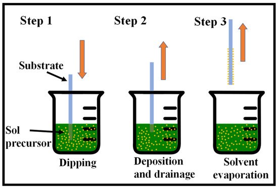
Figure 1. Sequential stages of the sol–gel dip-coating method for thin film deposition: Stage 1—the substrate is dipped and immersed in the sol precursor, Stage 2—the substrate is withdrawn at a steady rate, Stage 3—solvent evaporation produces the gelation of the layer.
The effectiveness of the dip-coating process can be directly impacted by several factors, such as pH and solution concentration, by changing, for example, its viscosity. However, as contemporary studies employ coating procedures that have already been documented in earlier works, most authors don’t talk much about pH and solution viscosity. Fewer repetitions of the dip-coating process are required to produce a certain thickness or amount of deposited mass when using more viscous solutions since they lead to greater agglomeration and thicker layers of coating [33]. However, the resultant coating could potentially break and clump particles in undesirable places. To obtain past these issues, the dip-coating technique can provide a more homogenous coating by using a less viscous solution in combination with multiple repeats. The structure’s rate of immersion in the solution is yet another factor that might affect the coating’s features [34]. A high rate of immersion, for example, may produce thicker layers because the solution’s viscous forces are increased, causing greater accumulation on the structure’s surface [35].
For thin-film coating techniques to be employed successfully in integrated optics, the film thickness must be completely under control. Because of this, thickness control is important for all thin-film development methods, including sol–gel. It has been reported that the coating speed, angle of inclination, and sol concentration have a major role in determining the ultimate thickness [36][37][38]. In addition, the ultimate heat-treated thickness can also be influenced by the sol viscosity, density, and liquid-vapor surface tension [39]. In [40], it is stated that a cleanroom atmosphere is required for the coating procedure to produce sol–gel thin films with great optical quality. To produce organic dye-doped thin films with tailored porosity for use in chemical sensing and optoelectronics, a three-step sol–gel procedure was developed [41]. Additionally, ceramic films generated from sol–gel are also presented in [24]. Here are some further important papers on the sol–gel technique [42][43][44][45][46][47][48][49][50][51].
Silica, titania, and silica-titania materials produced by the sol–gel technique have all undergone extensive research due to their potential optical uses [52][53][54][55][56][57]. The early part of the 1980s saw the beginning of their use in the production of silica-titania WG films. The first individuals to do so were Herrmann and Wildman. However, they used MERCK’s [53] commercially available liquid-coat solutions rather than synthetic sols. The research team led by Lukosz produced planar evanescent WG chemical/biochemical sensors utilizing these WG films, which were coated on glass substrates using the dip-coating technique and had refractive n = 1.8 at λ = 612.5 μm [54][55][56][58]. These films have optical losses of 2.5 dB/cm for λ = 632.8 μm [58]. Spin-coating was used by Jiwei et al. to fabricate SiO2-TiO2 WG films that were then coated on SiO2/Si (111) substrates [57]. The greatest refractive index of the films was n = 1.87 at λ = 632.8 μm, yet they had very significant optical losses of 7.4 dB/cm. It should be noted that 750 °C annealing temperatures were used to generate such a high refractive index value. The phase change from anatase to rutile is expected to occur at such high temperatures, making WG films much more lossy. There are also other studies [59][60][61][62] reporting the creation and characterization of composite SiO2-TiO2 films, although their waveguiding characteristics were not studied.
If the titania concentration is greater than 20 wt.%, the sol–gel-based manufacturing process of SiO2-TiO2 is quite challenging. This is due to titania’s great propensity to crystallize and produce distinct phases. As a result, manufactured films exhibit large optical losses and are not amorphous [63]. Another issue that causes optical losses to increase over time is long-term stability [64]. These challenges were overcome by Karasinski et al. by creating SiO2-TiO2 WG films with a 50% weight TiO2 content that are low-loss and long-term stable [23]. Using the dip-coating process on BK7 glass substrates, silica-titanium WG layers with a SiO2-TiO2 = 1:1 molar ratio were created, which were subsequently heated to 500 °C. The primary chemical precursors for silica SiO2 and titania TiO2 are tetraethyl orthosilicate Si (OC2H5)4 (TEOS) and tetraethyl orthotitanate Ti (OC2H5)4 (TET), respectively. Water, ethanol, and hydrochloric acid (HCl), which catalyzes the processes of condensation and hydrolysis, are the additional substances used in the procedure.
Moreover, Karasinski and co-workers produced a variety of films on glass substrates at various speeds to identify the key technical characteristic that demonstrates the link between the thickness and refractive index of waveguide films about the speed of substrate removal from the sol. After deposition, the films underwent a 60-min annealing process at 500 °C. Finally, using the monochromatic, multiangle ellipsometer Sentech SE 400 adv with a wavelength of 632.8 nm, the thickness and refractive index of those films were determined. Figure 2 displays the outcomes’ features [36]. From the parameters shown in Figure 2, a single coating procedure can only provide a maximum thickness of roughly 230 nm in the range of withdrawal speed shown. With the repeated coating method, thicker films may be created, which is important because the sample needs to be annealed after each coating. In order to determine the properties shown in Figure 2 of the set of ten SiO2-TiO2 waveguides that were created for this research in a single coating procedure, as well as a few more films in a double coating process.
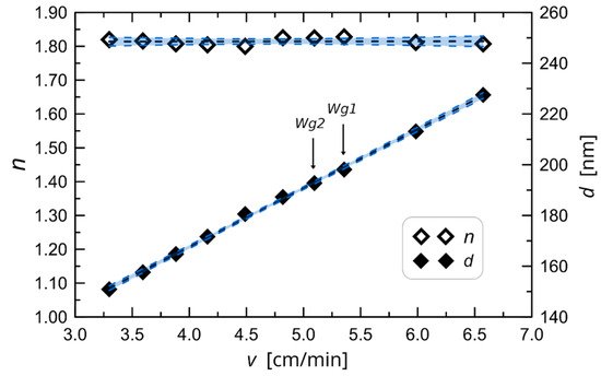
Figure 2. The experimentally determined characteristic of waveguide film thickness and refractive index against change in substrate withdrawal speed from the sol [36].
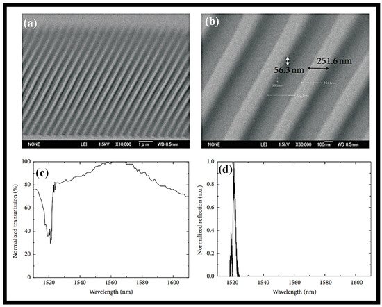
Nanoimprint lithography (NIL) is used to construct a Bragg grating (BG) device in a sol–gel silica WG for bio-photonic applications [65]. A reasonably wide area in the range of several micrometers with a resolution in the order of several nanometers is achieved by the procedure, which also achieves non-standardized lithography in sol–gel silica at a high resolution. In a sol–gel silica optical WG, structures with between 250 and 90 nm resolutions were shown for a sizable area that has not yet been tuned. For a 1 mm long region, a 250 nm periodic structure BG is produced. Two sol–gel silica BG structures, one measuring 250 nm broad and the other 90 nm wide, were then photographed using SEM as shown in Figure 3a,b. The transmission and reflection spectra of the BG structure are presented in Figure 3c,d, respectively. Based on the transmission and reflection spectra of laser light coupled into the WG at a wavelength of 1.55 µm, the efficiency of the grating structure in the WG was evaluated. The transmission and reflection spectra demonstrate that the WG grating was successfully constructed using the NIL procedure.
References
- Weinstein, S.; Ruschak, K. Coating flows. Annu. Rev. Fluid Mech. 2004, 36, 29–53.
- Krebs, F. Fabrication and processing of polymer solar cells: A review of printing and coating techniques. Sol. Energy Mater. Sol. Cells 2009, 93, 394–412.
- Konar, R.; Nessim, G. A mini-review focusing on ambient-pressure chemical vapor deposition (AP-CVD) based synthesis of layered transition metal selenides for energy storage applications. Mater. Adv. 2022, 3, 4471–4488.
- Rossnagel, S. Thin film deposition with physical vapor deposition and related technologies. J. Vac. Sci. Technol. A 2003, 21, S74.
- Johnson, R.; Hultqvist, A.; Bent, S. A brief review of atomic layer deposition: From fundamentals to applications. Materialstoday 2014, 17, 236–246.
- Hong, Y.-S.; Lee, S.-R.; Kim, J.-H.; Lee, S.-Y. Application of a DLC-coating for improving hydrostatic piston shoe bearing performance under mixed friction conditions. Int. J. Precis. Eng. Manuf. 2015, 16, 335–341.
- Tandon, P.; Boek, H. Experimental and theoretical studies of flame hydrolysis deposition process for making glasses for optical planar devices. J. Non-Cryst. Solids 2003, 317, 275–289.
- Ruano, J.M.; Benoit, V.; Aitchison, J.S.; Cooper, J.M. Flame hydrolysis deposition of glass on silicon for the integration of optical and microfluidic devices. Anal. Chem. 2000, 72, 1093–1097.
- Yang, Y.; Kim, K.-H.; Ong, J. A review on calcium phosphate coatings produced using a sputtering process: An alternative to plasma spraying. Biomaterials 2005, 26, 327–337.
- Orudzhev, F.; Ramazanov, S.; Sobola, D.; Isaev, A.; Wang, C.; Magomedova, A.; Kadiev, M.; Kaviyarasu, K. Atomic layer deposition of mixed-layered aurivillius phase on TiO2 nanotubes: Synthesis, characterization and photoelectrocatalytic properties. Nanomaterials 2020, 10, 2183.
- Dallaev, R.; Sobola, D.; Tofel, P.; Skvarenina, L.; Sedlak, P. Aluminum nitride nanofilms by atomic layer deposition using alternative precursors hydrazinium chloride and triisobutylaluminum. Coatings 2020, 10, 954.
- Butt, M.A.; Solé, R.; Pujol, M.C.; Ródenas, A.; Lifante, G.; Choudhary, A.; Murugan, G.S.; Shepherd, D.P.; Wilkinson, J.S.; Aguiló, M.; et al. Fabrication of Y-splitters and Mach-Zehnder structures on (Yb, Nb):RbTiOPO4/RbTiOPO4 epitaxial layers by reactive ion etching. J. Lightwave Technol. 2015, 33, 1863–1871.
- Butt, M.A.; Kozlova, E.S.; Khonina, S.N. Conditions of a single-mode rib channel waveguide based on dielectric TiO2/SiO2. Comput. Opt. 2017, 41, 494–498.
- Middleman, S. Fundamentals of Polymer Processing; McGraw-Hill: New York, NY, USA, 1977.
- Bird, R.; Dai, G.; Yarusso, B. The rheology and flow of viscoplastic materials. Rev. Chem. Eng. 1983, 1, 1–70.
- Jeong, J.; Lee, J.; Kim, H.; Kim, H.-K.; Na, S.-I. Ink-jet printed transparent electrode using nano-size indium tin oxide particles for organic photovoltaics. Sol. Energy Mater. Sol. Cells 2010, 94, 1840–1844.
- Eom, S.; Park, H.; Mujawar, S.; Yoon, S.; Kim, S.-S.; Na, S.; Kang, S.-J.; Khim, D.; Kim, D.-Y.; Lee, S.-H. High efficiency polymer solar cells via sequential inkjet-printing of PEDOT:PSS and P3HT:PCBM inks with additives. Org. Electron. 2010, 11, 1516–1522.
- Niu, X.; Li, N.; Chen, Q.; Zhou, H. Insights into large-scale fabrication methods in perovskite photovoltaics. Adv. Energy Sustain. Res. 2021, 2, 2000046.
- Voigt, M.; Mackenzie, R.; King, S.; Yau, C.; Atienzar, P.; Dane, J.; Keivanidis, P.; Zadrazil, I.; Bradley, D.; Nelson, J. Gravure printing inverted organic solar cells: The influence of ink properties on film quality and device performance. Sol. Energy Mater. Sol. Cells 2012, 105, 77–85.
- Kang, J.-W.; Kang, Y.-J.; Jung, S.; Song, M.; Kim, D.-G.; Kim, C.; Kim, S. Fully spray-coated inverted organic solar cells. Sol. Energy Mater. Sol. Cells 2012, 103, 76–79.
- Girotto, C.; Rand, B.; Genoe, J.; Heremans, P. Exploring spray coating as a deposition technique for the fabrication of solution-processed solar cells. Sol. Energy Mater. Sol. Cells 2009, 93, 454–458.
- Green, R.; Morfa, A. Performance of bulk heterojunction photovoltaic devices prepared by airbrush spray deposition. Appl. Phys. Lett. 2008, 92, 033301.
- Karasinski, P.; Tyszkiewicz, C.; Domanowska, A.; Michalewicz, A.; Mazur, J. Low loss, long time stable sol-gel derived silica-titania waveguide films. Mater. Lett. 2015, 143, 5–7.
- Brinker, C.J.; Frye, G.C.; Hurd, A.J.; Ashley, C.S. Fundamentals of sol-gel dip coating. Thin Solid Films 1991, 201, 97–108.
- Brinker, C.J.; Ashley, C.S.; Cairncross, R.A.; Chen, K.S.; Hurd, A.J.; Reed, S.T.; Samuel, J.; Schunk, P.R.; Schwartz, R.W.; Scotto, C.S. Sol-gel derived ceramic films-fundamentals and applications. In Metallurgical and Ceramic Protective Coatings; Stern, K.H., Ed.; Springer: Dordrecht, The Netherlands, 1996.
- Jaglarz, J.; Dulian, P.; Karasinski, P.; Winkowski, P. Scattering phenomena in porous sol-gel-derived silica films. Coatings 2020, 10, 509.
- Karasinski, P. Sol-gel derived optical waveguide films for planar sensors with phase modulation. Opt. Appl. 2004, 34, 467–475.
- Karasinski, P.; Tyszkiewicz, C.; Rogozinski, R. Rib waveguides based on the sol-gel derived SiO2:TiO2 films. Photonics Lett. Pol. 2010, 2, 40–42.
- Matsui, T.; Komatsu, K.; Sugihara, O.; Kaino, T. Simple process for fabricating a monolithic polymer optical waveguide. Opt. Lett. 2005, 30, 970–972.
- Killinger, A.; Gantenbein, G.; Illy, S.; Ruess, T.; Weggen, J.; Martinez-Garcia, V. Plasma spraying of a microwave absorber coating for an RF dummy load. Coatings 2021, 11, 801.
- Hongo, A.; Miyagi, M.; Kato, Y.; Suzumura, M.; Kubota, S.; Wang, Y.; Shimomura, T. Fabrication of dielectric-coated silver hollow glass waveguides for the infrared by liquid-flow coating method. In Proceedings of the Biomedical Fiber Optics, Photonics West, San Jose, CA, USA, 5 April 1996; Volume 2677.
- Faustini, M.; Louis, B.; Albouy, P.; Kuemmel, M.; Grosso, D. Preparation of sol−gel films by dip-coating in extreme conditions. J. Phys. Chem. C 2010, 114, 7637–7645.
- Hakki, H.; Allahyari, S.; Rahemi, N.; Tasbihi, M. Surface properties, adherence, and photocatalytic activity of sol-gel dip-coated TiO2-ZnO films on glass plates. C. R. Chim. 2019, 22, 393–405.
- Morais, D.; Boaventura, R.; Moreira, F.; Vilar, V. Advances in bromate reduction by heterogeneous photocatalysis: The use of a static mixer as photocatalyst support. Appl. Catal. B Environ. 2019, 249, 322–332.
- Zarubica, A. Modified nanostructured titania based thin films in photocatalysis: Kinetic and mechanistic approach. React. Kinet. Mech. Catal. 2015, 115, 159–174.
- Butt, M.; Tyszkiewicz, C.; Wojtasik, K.; Karasinski, P.; Kazmierczak, A.; Piramidowicz, R. Subwavelength grating waveguide structures proposed on the low-cost silica-titania platform for optical filtering and refractive index sensing applications. Int. J. Mol. Sci. 2022, 23, 6614.
- Butt, M.; Kazmierczak, A.; Tyszkiewicz, C.; Karasinski, P.; Piramidowicz, R. Mode sensitivity exploration of silica-titania waveguide for refractive index sensing applications. Sensors 2021, 21, 7452.
- Butt, M.; Tyszkiewicz, C.; Karasinski, P.; Zieba, M.; Hlushchenko, D.; Baraniecki, T.; Kazmierczak, A.; Piramidowicz, R.; Guzik, M.; Bachmatiuk, A. Development of a low-cost silica-titania optical platform for integrated photonics applications. Opt. Express 2022, 30, 23678.
- Schroeder, H. Oxide layers deposited from organic solutions. In Physics of Thin Films: Advances in Research and Developments; Academic Press: New York, NY, USA; London, UK, 1969; pp. 87–141.
- Attia, S.M.; Wang, J.; Wu, G.; Shen, J.; Jianhua, M.A. Review on sol-gel derived coatings: Process, techniques and optical applications. J. Mater. Sci. Technol. 2002, 18, 211–217.
- Logan, M.N.; Prabakar, S.; Brinker, C.J. Sol-gel-derived silica films with tailored microstructures for applications requiring organic dyes. MRS Online Proc. Libr. 1994, 346, 115–120.
- Fidalgo, A.; Ilharco, L.M. The defect structure of sol-gel-derived silica/polytetrahydrofuran hybrid films by FTIR. J. Non-Cryst. Solids 2001, 283, 144–154.
- Parin, R.; Rigon, M.; Bortolin, S.; Martucci, A.; Col, D.D. Optimization of hybrid sol-gel coating for dropwise condensation of pure steam. Materials 2020, 13, 878.
- Acosta, S.; Ayral, A.; Guizard, C.; Lecornec, C.; Passemard, G.; Moussavi, M. Sol-gel derived silica layers for low-k dielectrics applications. MRS Online Proc. Libr. 2000, 612, 5261.
- Boudot, M.; Gaud, V.; Louarn, M.; Selmane, M.; Grosso, D. Sol-Gel based hydrophobic antireflective coatings on organic substrates: A detailed investigation of Ammonia Vapor Treatment (AVT). Chem. Mater. 2014, 26, 1822–1833.
- Kim, T.; Song, K. Low-temperature preparation of superhydrophilic coatings using tetraethoxysilane and colloidal silica by sol-gel method. Colloids Surf. A Physicochem. Eng. Asp. 2022, 647, 129105.
- Hasaneen, M.; Shalaby, M.; Yousif, N.; Diab, A.; Agammy, E. Structural and optical properties of transparent conducting oxide Cd1-xCrxO thin films prepared by the sol-gel dip-coating method. Mater. Sci. Eng. B 2022, 280, 115703.
- Niazmand, M.; Maghsoudipour, A.; Alizadeh, M.; Khahpour, Z.; Kariminejad, A. Effect of dip coating parameters on microstructure and thickness of 8YSZ electrolyte coated on NiO-YSZ by sol-gel process for SOFCs applications. Ceram. Int. 2022, 48, 16091–16098.
- Esfahani, M.; Eshaghi, A.; Bakhshi, S. Transparent hydrophobic, self-cleaning, anti-icing and anti-dust nano-structured silica based thin film on cover glass solar cell. J. Non-Cryst. Solids 2022, 583, 121479.
- Beldjebli, O.; Bensaha, R.; Panneerselvam, P. Effect of both Sn doping and annealing temperature on the properties of dip-coated nanostructured TiO2 thin films. J. Inorg. Organomet. Polym. Mater. 2022, 32, 1624–1636.
- Both, J.; Szabo, G.; Katona, G.; Muresan, L. Tannic acid reinforced sol-gel silica coatings for corrosion protecion of zinc substrates. Mater. Chem. Phys. 2022, 282, 125912.
- Karasinski, P.; Tyszkiewicz, C.; Piramidowicz, R.; Kazmierczak, A. Development of integrated photonics based on SiO2:TiO2 sol-gel derived waveguide layers:state of the art, perspectives, prospective applications. Integr. Photonics Platf. Fundam. Res. Manuf. Appl. 2020, 11364, 1136414.
- Hermann, P.; Wildmann, D. Fabrication of planar dielectric waveguides with high optical damage threshold. IEEE J. Quantum Electron. 1983, 19, 1735–1738.
- Lukosz, W.; Tiefenthaler, K. Embossing technique for fabricating integrated optical components in hard inorganic waveguiding materials. Opt. Lett. 1983, 8, 537–539.
- Tiefenthaler, K.; Lukosz, W. Sensitivity of grating couplers as integrated-optical chemical sensors. J. Opt. Soc. Am. B 1989, 6, 209–220.
- Clerc, D.; Lukosz, W. Direct immunosensing with an integrated-optical output grating coupler. Sens. Actuators B 1997, 40, 53–58.
- Jiwei, Z.; Xi, Y.; Liangying, Z. Characterization and optical propagtion loss of sol-gel derived TiO2/SiO2 films. J. Phys. D Appl. Phys. 2000, 33, 3013–3017.
- Tiefenthaler, K.; Briguet, V.; Buser, E.; Horisberger, M.; Lukosz, W. Preparation of planar optical SiO2-TiO2 and LiNbO3 waveguides with a dip coating method and embossing technique for fabricating grating couplers and channel waveguides. Proc. SPIE 1983, 401, 165–173.
- Chrysicopoulou, P.; Davazoglou, D.; Trapalis, C.; Kordas, G. Optical properties of SiO2-TiO2 sol-gel thin films. J. Mater. Sci. 2004, 39, 2835–2839.
- Wang, X.; Wu, G.; Zhou, B.; Shen, J. Thermal annealing effect on optical properties of binary TiO2-SiO2 sol-gel coatings. Materials 2013, 6, 76–84.
- Kermadi, S.; Agoudjil, N.; Sali, S.; Zougar, L.; Boumaour, M.; Broch, L.; Placido, F. Microstructure and optical dispersion characterization of nanocomposite sol–gel TiO2–SiO2 thin films with different compositions. Spectrochim. Acta Part A Mol. Biomol. Spectrosc. 2015, 145, 145–154.
- Lukowiak, A.; Dylewicz, R.; Patela, S.; Strek, W.; Maruszewski, K. Optical properties of SiO2-TiO2 thin film waveguides obtained by the sol-gel method and their applications for sensing purposes. Opt. Mater. 2005, 27, 1501–1505.
- Almeida, R.; Morais, P.; Vasconcelos, H. Optical loss mechanism in nanocomposite sol-gel planar waveguides. In Proceedings of the SPIE, Sol-Gel Optics IV, San Diego, CA, USA, 30 July–1 August 1997; pp. 296–303.
- Weisenbacht, L.; Zelinski, B. The attenuation of sol-gel waveguides measured as a function of wavelength and sample age. In Proceedings of the SPIE 2288 Sol-Gel Optics III, San Diego, CA, USA, 13 October 1994; pp. 630–639.
- Enami, Y. Fabricating 90 nm resolution structures in sol-gel silica optical waveguides for biosensor applications. J. Sens. 2017, 2017, 4198485.
More
Information
Subjects:
Physics, Fluids & Plasmas
Contributor
MDPI registered users' name will be linked to their SciProfiles pages. To register with us, please refer to https://encyclopedia.pub/register
:
View Times:
9.2K
Revisions:
2 times
(View History)
Update Date:
10 Aug 2022
Table of Contents


Notice
You are not a member of the advisory board for this topic. If you want to update advisory board member profile, please contact office@encyclopedia.pub.
OK
Confirm
Only members of the Encyclopedia advisory board for this topic are allowed to note entries. Would you like to become an advisory board member of the Encyclopedia?
Yes
No
${ textCharacter }/${ maxCharacter }
Submit
Cancel
Back
Comments
${ item }
|
${ item.createdUser.fullName }
${ item.createdAt }
${ item.vote }
${ item.reply }
Delete
${ reply.createdUser.fullName }
${ reply.createdAt }
${ reply.vote }
Delete
There is no reply to this comment~
${ item.replyTextCharacter }/${ item.replyMaxCharacter }
Submit
Cancel
More
No more~
There is no comment~
${ textCharacter }/${ maxCharacter }
Submit
Cancel
${ selectedItem.replyTextCharacter }/${ selectedItem.replyMaxCharacter }
Submit
Cancel
Confirm
Are you sure to Delete?
Yes
No