Your browser does not fully support modern features. Please upgrade for a smoother experience.
Submitted Successfully!
 +1 credit
Thank you for your contribution! You can also upload a video entry or images related to this topic.
For video creation, please contact our Academic Video Service.
Video Upload Options
We provide professional Academic Video Service to translate complex research into visually appealing presentations. Would you like to try it?
Cite
If you have any further questions, please contact Encyclopedia Editorial Office.
Wang, M.; Xiao, Y.; Li, Y.; Han, L.; Sun, Z.; He, L.; Liu, R.; Hu, K. Graphene Flexible Photodetectors. Encyclopedia. Available online: https://encyclopedia.pub/entry/25623 (accessed on 26 July 2026).
Wang M, Xiao Y, Li Y, Han L, Sun Z, He L, et al. Graphene Flexible Photodetectors. Encyclopedia. Available at: https://encyclopedia.pub/entry/25623. Accessed July 26, 2026.
Wang, Mengzhu, Yingying Xiao, Ye Li, Lu Han, Zhicheng Sun, Liang He, Ruping Liu, Kuan Hu. "Graphene Flexible Photodetectors" Encyclopedia, https://encyclopedia.pub/entry/25623 (accessed July 26, 2026).
Wang, M., Xiao, Y., Li, Y., Han, L., Sun, Z., He, L., Liu, R., & Hu, K. (2022, July 28). Graphene Flexible Photodetectors. In Encyclopedia. https://encyclopedia.pub/entry/25623
Wang, Mengzhu, et al. "Graphene Flexible Photodetectors." Encyclopedia. Web. 28 July, 2022.
Copy Citation
In recent years, optoelectronics and related industries have developed rapidly. As typical optoelectronics devices, photodetectors (PDs) are widely applied in various fields. The functional materials in traditional PDs exhibit high hardness, and the performance of these rigid detectors is thus greatly reduced upon their stretching or bending.
graphene
photodetector
1. Introduction
With the development of modern communication technology and the Internet of Things (IoT), devices with high foldability, wearability, and bending resistance have been increasingly developed, and there are in-depth studies on flexible optoelectronic devices. Flexible photodetectors (PDs) can be bent, folded, or even stretched, and their applications in imaging, display, optical communications, medical care, and other fields are drawing increasing attention, as they are highly useful in electronic skin, smart textiles, electronic eyes, and flexible cameras [1][2][3][4]. There are usually three components in flexible PDs: flexible substrate, flexible electrode, and functional material. Carbon fiber cloth, fiber, paper, and many polymers, such as polyethylene terephthalate (PET), polyimide (PI), and polydimethylsiloxane (PDMS), are the most commonly used flexible substrates. These widely used substrates for flexible PDs have unique flexibility, high mechanical stability, and high chemical stability [5][6][7]. Indium tin oxide (ITO), as a flexible electrode, is widely used in displays. However, due to its inherent fragility, alternatives to this material have been developed, such as conductive polymers and metal nanowires, among which transparent conductive graphene films have been widely studied in recent years. The functional components in flexible PDs include materials such as two-dimensional (2D) perovskites and 2D metal halides [8][9]. Flexible PDs should maintain stable performance during repeated bending, folding, or stretching [10], placing a high demand on the mechanical stability and flexibility of their component electrodes and functional materials. Due to their adjustable bandgap, high light absorption efficiency, electron mobility, and low sensitivity to their environment, carbon materials have great potential in the field of PDs [11]. Graphene was the first known 2D layered material, with its discovery leading to a research boom due to its high flexibility, extraordinary elastic modulus, and large strain (>10%). Furthermore, optically transparent graphene exhibits high carrier mobility, and its optical performance can be adjusted via electrostatic doping or strain to realize flexible electronic devices with novel functions. In addition, the high carrier mobility of graphene ensures the ultrafast conversion of photons or plasmons into electrical signals, which is very helpful for producing ultrasensitive PDs exhibiting high photoconductivity gain [12][13]. In graphene-based PDs, to achieve effective light capture, it is necessary to increase the light absorption rate, establish a suitable band structure, and improve the quality of the interface. When graphene-based PDs were first studied, the main focus was on analyzing the structures of field-effect transistors. Early studies showed that the light response rate of these PDs was generally < 0.01 A/W [14][15]. In recent years, many studies have been carried out to improve the performance of graphene PDs, with many studies focused on the preparation of graphene conductive films. As one of the most important parts of a PD, the performance of graphene determines the device’s performance.
2. Two-Dimensional Graphene
Carbon-based materials, such as diamond, graphite, and amorphous carbon, have broad applications. New carbon materials, including zero-dimensional (0D) fullerenes, one-dimensional (1D) carbon nanotubes (CNTs), and 2D graphene, have gradually evolved into the most promising carbon nanomaterials. Graphene is a single-layer sheet of graphite, which is the matrix of other allotropes of carbon, such as fullerenes, CNTs, and graphite [16][17][18][19]. It is a stable 2D atomic crystalline material formed from covalently bonded carbon atoms, arranged in a honeycomb lattice, and has a unique Dirac tapered energy band structure. The thickness of this monoatomic layer of graphite is approximately 0.335 nm [20][21]. In 2004, at the University of Manchester, Novoselov and Geim used a tape stripping method to strip graphene from graphite crystals and prepare graphene devices, and there has been exponential progress in the study of graphene for applications in various electronic devices [22].
Due to its 2D structure, graphene has unique physical properties, such as high electrical conductivity and high light transmission. Ultrathin graphene also exhibits high chemical stability, high ductility, and high mechanical strength, e.g., monolayer graphene has a high Young’s modulus of 1.0 TPa and a tensile strength of 130 GPa [20]. Graphene was the first 2D material prepared to exist stably at room temperature. These excellent characteristics make it widely applied in photoelectric detection. Since graphene is a semimetallic material with no gap, it has an ultrahigh carrier mobility of as high as 20,000 cm2/(V·s) at low temperatures [22], a value that is 10 times greater than those of silicon materials and twice that of indium antimonide (InSb), which has the highest known carrier mobility, as the electron mobility of graphene is less affected by temperature. At any temperature in the range of 50–500 K, the electron mobility of monolayer graphene is approximately 15,000 cm2/(V·s) [23][24]. Graphene can maximize the gain of PD devices and exhibits a wide response range across the entire electromagnetic spectrum. Due to its zero bandgap, it can absorb light over a wide spectrum (from the visible to terahertz (THz) regions) [20][21], providing the possibility of light detection over a wide spectral range. To the best of knowledge, it is the only known conductive material that exhibits high transparency across the entirety of the infrared (IR) region of the spectrum (including the mid-to-far IR), as shown in Figure 1. The excellent ductility of graphene also expands its application prospects in flexible optoelectronic devices, and it is expected to have broad development prospects in the fields of electronics, photonics, energy, environmental protection, and biomedicine.
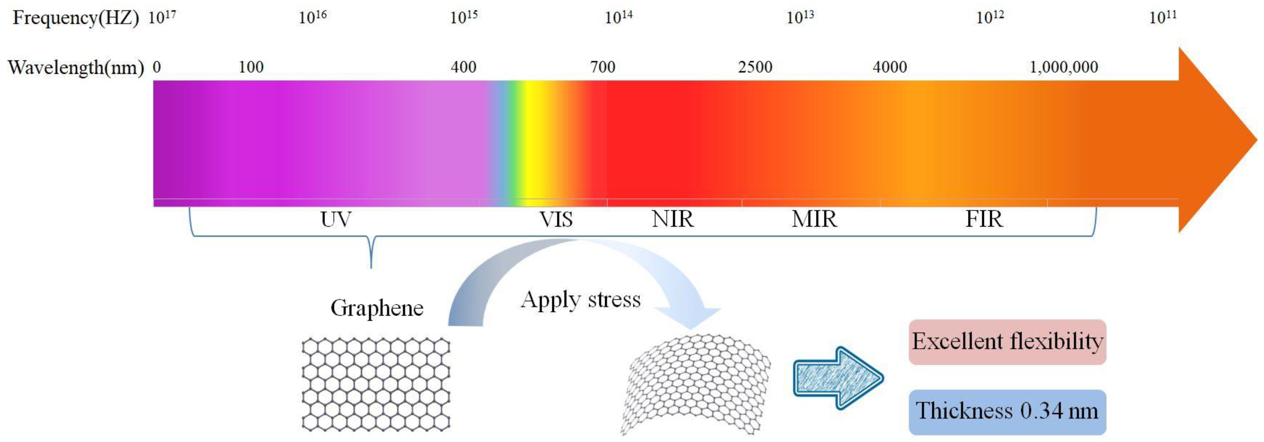
Figure 1. Bandgap values of various 2D materials and their corresponding detection ranges. Detection range and properties of two-dimensional material graphene.
2.1. Preparation of Graphene Transparent Conductive Films
At present, the crystal domain size of graphene films is mostly from micrometers to millimeters, and it can even reach the centimeter level [25]. The current trend in the development of graphene films is to develop the controllable, rapid preparation of graphene films with a large area and large crystal domains via high-quality in situ deposition [26]. Due to the interlayer aggregation of graphene and its small active area (~100 μm2), it is difficult to realize uniform deposition on the required substrate. Therefore, the efficiency of graphene-based (Transparent Conductive Films) TCFs is generally lower than that of commercially available transparent conductive oxides. Graphene films used in photoelectric detection not only need to be highly efficient but must also be uniform without agglomeration [27]. Recently, the Li research group proposed a new solution to eliminate the problem of graphene wrinkles. The study found that a high proportion of hot hydrogen can overcome the force between graphene and the substrate to a certain extent, with the protons and electrons in the hydrogen passing through the graphene layer, which makes the prepared multilayer (ML) graphene exhibit better layering, with an almost wrinkle-free appearance [28].
Although the development prospects of graphene films are great, the large-area and high-quality preparation of graphene films remains a critical challenge. Graphene was originally obtained via the mechanical exfoliation of graphite flakes. At present, a series of preparation methods for graphene have been developed, including liquid-phase exfoliation, reduction of graphene oxide, epitaxial growth of silicon carbide (SiC) or metal single crystals, molecular assembly, and CVD, among others [22][29]. The graphene prepared via mechanical exfoliation is of high quality, but its small size and low yield limit its wide application. A large amount of graphene can be prepared by chemical reduction, but its electrical performance is relatively low. Wafer-thin graphene can be prepared through SiC epitaxy, but it does not meet the requirements of large-area flexible electronic devices, and it is difficult to transfer the graphene attached to the SiC substrate to a flexible substrate. Molecular assembly is an expensive method, meaning that graphene prepared in this way does not meet the requirements of low-cost flexible electronic devices [30].
These methods are thus not suitable for application in flexible electronic devices. CVD is another effective technology for synthesizing large-area graphene films. At present, this technology is being widely studied in the field of graphene film preparation [31]. In the CVD process, gaseous or vaporous substances react in the gas phase or on a gas–solid interface to generate solid deposits. The preparation of graphene films via CVD usually requires a high-temperature furnace. Under high-temperature conditions of approximately 1000 °C, carbon-containing precursors such as methane are used as carbon sources to pass into the high-temperature chamber, and processes such as carbon source cracking, surface diffusion of activated carbon species, and graphene nucleation growth occur on the substrate, finally leading to a graphene film being deposited on the substrate [27].
Thermal CVD of graphene involves the use of first-row transition metals, such as iron (Fe) [32], cobalt (Co) [33], nickel (Ni) [34], and copper (Cu) [35][36] as catalysts. The solubility of carbon in these metals is the main parameter that affects growth quality. Among them, Fe has the highest solubility and Cu has the lowest solubility. Therefore, Cu is the preferred catalytic metal for the growth of monolayer graphene. In 2009, the Ruoff group successfully prepared a large-area graphene film on Cu foil (25 μm) for the first time via CVD. This process can be used to grow graphene on a 300 mm copper film on a silicon substrate, which is a very important technological breakthrough [29]. The film has the advantages of high quality and good controllability. Since then, the road to large-scale preparation of high-quality graphene films has opened up. For a long time, CVD was considered to be the most promising method for preparing large-area high-quality graphene films. However, as the size of the reactor increases, there are significant increases in manufacturing difficulties and the cost of CVD reactors, which in turn lead to limitations on the size and throughput of graphene films [37]. In addition, the high-temperature CVD growth of graphene is accompanied by some side reactions, leading to a large amount of amorphous carbon contaminants being deposited on the surface of graphene, leading to “intrinsic pollution” of the graphene film, which seriously affects the performance of graphene. Currently, there is still a large discrepancy between the measured performance of graphene films and the values expected from theory, indicating that research is required to improve the performance of graphene films [38][39]. Wang et al. [37] reported a “breathing” CVD method, in which a spiral Cu foil as substrate is employed to increase the loading density. In this process, graphite spacers are placed between the Cu layers at both ends of the spiral to prevent the Cu layers from adhering together at high temperature. There is enough space inside the spiral substrate, and the reaction gas is inhaled by cyclically adjusting the rise and fall of the pressure in the reactor and the Cu spiral of the auxiliary gas exchange. This method is similar to breathing, effectively using the space of a small reactor, and the size and throughput of the prepared graphene film is an order of magnitude higher than that of traditional methods. To date, the temperature required in most reported CVD methods is above 1000 °C to achieve the complete preparation of graphene. Aside from it being a time-consuming and high-cost method, the most important point about CVD is that it is not suitable for basic materials that are not resistant to high temperature. Recently, a new CVD method has been developed that is different from traditional processes. The new method utilizes molten gallium as a catalyst and sapphire and polycarbonate as substrates. Using this method, graphene can be grown at approximately 50 °C. This technology can therefore overcome the high-temperature requirement of traditional preparation methods [40][41].
2.2. Transfer Technology of Transparent Conductive Graphene Films
The preparation of high-quality graphene is an important issue in the practical applications of graphene. Simultaneously, transfer of graphene is also an indispensable process, which is closely related to the realization of large-scale production of graphene films. For application of graphene in PDs, it needs to be transferred to a target substrate that is suitable for the device. Due to the limitations of technology and preparation conditions, it is difficult to obtain clean graphene via a direct growth method, and the transfer process makes the film even dirtier. Many impurities are deposited on the surface of the film, which have an adverse effect on the performance of the device. Therefore, the surface contamination of graphene is a critical and unresolved challenge [39]. In addition, the transfer process of graphene is also complicated, as graphene is prone to the formation of wrinkles, folds, or defects during its transfer process, all of which reduce its transfer efficiency. The transfer of graphene can be divided into two categories: direct transfer and indirect transfer.
2.3. Indirect Transfer Method
Using a carrier material as a supporting layer, after the graphene is transferred from the growth substrate to the target substrate, the carrier material is removed through physical or chemical methods to complete the transfer. The common method is using polymethyl methacrylate (PMMA) as the carrier to obtain the transfer of graphene grown on the surface of Cu foil. PMMA has high flexibility and high solubility in a variety of organic solvents, but its most important property is high transparency, which is beneficial for clearly observing the removal process of the Cu foil [42]. However, this method will easily lead to damage and wrinkling of the graphene. PDMS can also be used for transfer [24]. A benefit of using PDMS is its lower surface energy compared to that of PMMA, making it easier to separate the polymer from graphene after its transfer. Zhang et al. [43] selected slow-adsorption and low-cost rosin as a support layer to complete the clean and structure-intact transfer of large-sized graphene and successfully produced a single-chip flexible organic light-emitting diode (OLED). Leong et al. [44] took advantage of the stable chemical properties of paraffin and non-covalent adsorption, replacing PMMA with paraffin to achieve high-quality transfer of graphene. Through a combination of the roll-to-roll technique and other automated processes, the temperature during transfer can be well controlled, and the efficiency and production yield of transfer can be greatly improved. Additionally, through reasonable selection of the carrier and continuous optimization of the process, indirect transfer can be carried out to obtain high-quality graphene. In theory, this method can be used to transfer graphene to any substrate and has a wide range of applications.
2.4. Direct Transfer Method
Using this method, graphene is directly attached to the target substrate and peeled off from the growth substrate to complete the transfer without the need for any carrier materials. The principles behind this method are that after the target substrate is processed, the binding force between graphene and the target substrate is much larger than the binding force between graphene and the growth substrate, with the growth substrate then being removed via etching or direct peeling. In 2012, Yoon et al. [45] used epoxy resin (EpoTek 353ND) to directly peel off graphene from a Cu substrate and used a double cantilever beam (DCB)-based fracture mechanics test to directly measure the adhesion between graphene and the Cu substrate for the first time, which proved that the direct transfer of graphene from the Cu substrate to the target substrate could be achieved. Compared with the indirect transfer method, the direct transfer method has no need to remove the carrier due to the addition of an assistant interlayer, and cracks will not be introduced in the graphene due to its spontaneous relaxation issues during the degumming process, greatly reducing the damage rate of the graphene film, and thus making it stronger. However, attention needs to be paid to the issue that the adhesion interlayer cannot have a great negative effect on the performance of graphene. Considering that the interlayer is inevitably a source of pollution, studies are also focused on attempts to directly transfer graphene to the target substrate without the assistance of a polymer. For example, Lin et al. [46] proposed adding isopropanol to adjust the surface tension of etchants to protect graphene from tearing, thereby realizing direct carrier-free transfer. However, most of these methods require strict experimental conditions, which are limited by the film size, equipment, substrate, and other conditions; therefore, production efficiency and cost cannot be balanced.
For the transfer of graphene, the solution processing of graphene offers various facile processes, such as spin, dip, and spray coating. The production cost of this method is relatively low and involves the use of fewer chemicals. However, overall, the high-quality, uniform, easy-to-process, and low-cost transfer of graphene is still challenging and requires further exploration to meet industrial and market demands [47].
References
- Wang, Y.; Sun, L.; Wang, C.; Yang, F.; Ren, X.; Zhang, X.; Dong, H.; Hu, W. Organic crystalline materials in flexible electronics. Chem. Soc. Rev. 2019, 48, 1492–1530.
- Han, S.T.; Peng, H.; Sun, Q.; Venkatesh, S.; Chung, K.S.; Lau, S.C.; Zhou, Y.; Roy, V.A.L. An Overview of the Development of Flexible Sensors. Adv. Mater. 2017, 29, 1700375.
- Dong, T.; Simões, J.; Yang, Z. Flexible photodetector based on 2D materials: Processing, architectures, and applications. Adv. Mater. Interfaces 2020, 7, 1901657.
- Ali, A.; Shehzad, K.; Guo, H.; Wang, Z.; Wang, P.; Qadir, A.; Hu, W.; Ren, T.; Yu, B.; Xu, Y. High-performance, flexible graphene/ultra-thin silicon ultra-violet image sensor. In Proceedings of the 2017 IEEE International Electron Devices Meeting (IEDM), San Francisco, CA, USA, 2–6 December 2017; IEEE: Manhattan, NY, USA, 2017; Volume 12, pp. 861–864.
- Sun, H.; Tian, W.; Cao, F.; Xiong, J.; Li, L. Ultrahigh-Performance Self-Powered Flexible Double-Twisted Fibrous Broadband Perovskite Photodetector. Adv. Mater. 2018, 30, 1706986.
- Qian, L.; Sun, Y.; Wu, M.; Li, C.; Xie, D.; Ding, L.; Shi, G. A lead-free two-dimensional perovskite for a high-performance flexible photoconductor and a light-stimulated synaptic device. Nanoscale 2018, 10, 6837–6843.
- Fang, H.; Li, J.; Ding, J.; Yue, S.; Li, Q. An Origami Perovskite Photodetector with Spatial Recognition Ability. Appl. Mater. Interfaces 2017, 9, 10921–10928.
- Hossain, R.F.; Bandyopadhyay, A.S.; Kaul, A.B. Vibrational spectroscopy on solution-dispersed MoS2 for inkjet-printed photodetectors. Emergent Mater. 2022, 5, 477–487.
- Ge, Z.; Xu, N.; Zhu, Y.; Zhao, K.; Ma, Y.; Li, G.; Chen, Y. Visible to Mid-Infrared Photodetection Based on Flexible 3D Graphene/Organic Hybrid Photodetector with Ultrahigh Responsivity at Ambient Conditions. ACS Photonics 2022, 9, 59–67.
- Liu, Y.F.; Feng, J.; Bi, Y.G.; Yin, D.; Sun, H.B. Recent Developments in Flexible Organic Light-Emitting Devices. Adv. Mater. Technol. 2019, 4, 1800371.
- Chen, M. The Basic Category and Application of Graphene-Based Hybrid Photodetector; IOP Conference Series: Earth and Environmental Science; IOP Publishing: Bristol, UK, 2021; p. 052092.
- Chen, X.; Shehzad, K.; Gao, L.; Long, M.; Guo, H.; Qin, S.; Wang, X.; Wang, F.; Shi, Y.; Hu, W.; et al. Graphene Hybrid Structures for Integrated and Flexible Optoelectronics. Adv. Mater. 2020, 32, e1902039.
- Chen, G.; Zhou, Y.; Zhang, G.; Li, J.; Qi, X. Flexible, self-powered Bi2O2Se/Graphene photoeletrochemical photodetector based on solid-state electrolytes. Ceram. Int. 2021, 47, 25255–25263.
- De Sanctis, A.; Jones, G.F.; Wehenkel, D.J.; Bezares, F.; Koppens, F.H.L.; Craciun, M.F.; Russo, S. Extraordinary linear dynamic range in laser-defined functionalized graphene photodetectors. Sci. Adv. 2017, 3, e1602617.
- Khosravian, E.; Mashayekhi, H.R.; Farmani, A. Tunable plasmonics photodetector in near-infrared wavelengths using graphene chemical doping method. AEU Int. J. Electron. Commun. 2020, 127, 153472.
- Andreoni, W. The Physics of Fullerene-Based and Fullerene-Related Materials; Springer: Dordrecht, The Netherlands, 2000; Volume 23, p. 448.
- Charlier, J.C.; Blase, X.; Roche, S. Electronic and transport properties of nanotubes. Rev. Mod. Phys. 2007, 79, 677.
- Salvetat, J.P.; Bonard, J.M.; Bacsa, R. Physical Properties of Carbon Nanotubes; World Book Publishing Company: Chicago, IL, USA, 1998.
- Petroski, H. Technology of the Ubiquitous. Science 1990, 248, 23106.
- Lee, C.; Wei, X.; Kysar, J.W.; Hone, J. Measurement of the Elastic Properties and Intrinsic Strength of Monolayer Graphene. Science 2008, 321, 385–388.
- Novoselov, S.; Morozov, K.; Mohinddin, S.V.; Castro, T.M.G.; Neto, A.C.; Guinea, F. The electronic properties of graphene. Rev. Mod. Phys. 2009, 81, 109.
- Novoselov, K.S.; Geim, A.K.; Morozov, S.V.; Jiang, D.; Zhang, Y.; Dubonos, S.V.; Grigorieva, I.V.; Firsov, A.A. Electric field effect in atomically thin carbon films. Science 2004, 306, 666–669.
- Bolotin, K.I.; Sikes, K.J.; Jiang, Z.; Klima, M.; Fudenberg, G.; Hone, J.; Kim, P.; Stormer, H.L. Ultrahigh electron mobility in suspended graphene. Solid State Commun. 2008, 146, 351–355.
- Kim, K.S.; Yue, Z.; Jang, H.; Sang, Y.L.; Hong, B. Large-scale pattern growth of graphene films for stretchable transparent electrodes. Nature 2009, 457, 706–710.
- Gürsoy, M.; Tak, E.; Karaman, M. Uniform deposition of large-area graphene films on copper using low-pressure chemical vapor deposition technique. Carbon Lett. 2022, 32, 781–787.
- Yanru, H.; Xiaorang, T.; Guanchao, Z.; Lingling, D.; Ge, N.; Minsheng, L. Research Progress in Preparation and Applications of Graphene Films. Mater. Guide 2020, 34, 5048–5060.
- Chen, H.; Zhang, J.; Liu, X.; Liu, Z. Effect of Gas-Phase Reaction on the CVD Growth of Graphene. J. Phys. Chem. 2021, 7, 2101053.
- Zhang, W.; Chuu, C.P.; Huang, J.-K.; Chen, C.-H.; Tsai, M.-L.; Chang, Y.-H.; Liang, C.-T.; Chen, Y.-Z.; Chueh, Y.-L.; He, J.-H.; et al. Ultrahigh-Gain Photodetectors Based on Atomically Thin Graphene-MoS2 Heterostructures. Sci. Rep. UK 2014, 4, 3826.
- Li, X.; Cai, W.; An, J.; Kim, S.; Nah, J.; Yang, D.; Piner, R.; Velamakanni, A.; Jung, I.; Tutuc, E. Large-Area Synthesis of High-Quality and Uniform Graphene Films on Copper Foils Science. Science 2009, 324, 1312–1314.
- Hackley, J.; Ali, D.; DiPasquale, J.; Demaree, J.D.; Richardson, C.J.K. Graphitic carbon growth on Si(111) using solid source molecular beam epitaxy. Appl. Phys. Lett. 2009, 95, 133114.
- Li, X.; Colombo, L.; Rodney, S.; Ruoff, R.S. Synthesis of Graphene Films on Copper Foils by Chemical Vapor Deposition. Adv. Mater. 2016, 28, 6247–6252.
- An, H.; Lee, W.J.; Jung, J. Graphene synthesis on Fe foil using thermal CVD. Curr. Appl. Phys. 2011, 11, S81–S85.
- Ago, H.; Ito, Y.; Mizuta, N.; Yoshida, K.; Hu, B.; Orofeo, C.M.; Tsuji, M.; Ikeda, K.I.; Mizuno, S. Epitaxial Chemical Vapor Deposition Growth of Single-Layer Graphene over Cobalt Film Crystallized on Sapphire. ACS Nano 2010, 4, 7407–7414.
- Reina, A.; Jia, X.; Ho, J.; Nezich, D.; Son, H.; Bulovic, V.; Dresselhaus, M.S.; Kong, J. Large area, few-layer graphene films on arbitrary substrates by chemical vapor deposition. Nano Lett. 2009, 9, 30–35.
- Guermoune, A.; Chari, T.; Popescu, F.; Sabri, S.S.; Guillemette, J.; Skulason, H.S.; Szkopek, T.; Siaj, M. Chemical vapor deposition synthesis of graphene on copper with methanol, ethanol, and propanol precursors—ScienceDirect. Carbon 2011, 49, 4204–4210.
- Chen, X.; Zhang, L.; Chen, S. Large area CVD growth of graphene. Synth. Met. 2015, 210, 95–108.
- Wang, Y.; Qing, F.Z.; Jia, Y.; Duan, Y.W.; Shen, C.Q.; Hou, Y.T.; Niu, Y.T.; Shi, H.F.; Li, X.S. Synthesis of large-area graphene films on rolled-up Cu foils by a “breathing” method. Chem. Eng. J. 2021, 405, 127014.
- Zhang, J.; Sun, L.; Jia, K.; Liu, X.; Cheng, T.; Peng, H.; Lin, L.; Liu, Z. New Growth Frontier: Superclean Graphene. ACS Nano 2020, 14, 10796–10803.
- Lin, L.; Zhang, J.; Su, H.; Li, J.; Sun, L.; Wang, Z.; Xu, F.; Liu, C.; Lopatin, S.; Zhu, Y.; et al. Towards super-clean graphene. Nat Commun. 2019, 10, 1912.
- Khan, A.; Habib, M.R.; Kumar, R.R.; Islam, S.M.; Arivazhagan, V.; Salman, M.; Yang, D.R.; Yu, X.G. Wetting behaviors and applications of metal-catalyzed CVD grown graphene. J. Mater. Chem. A 2018, 6, 22437–22464.
- Kang, M.H.; Qiu, G.Y.; Chen, B.A.; Jouvray, A.; Teo, K.B.K.; Cepek, C.; Wu, L.; Kim, J.; Milne, W.I.; Cole, M.T. Transport in polymer-supported chemically-doped CVD graphene. J. Mater. Chem. C 2017, 5, 9886–9897.
- Jiao, L.; Fan, B.; Xian, X.; Wu, Z.; Zhang, J.; Liu, Z. Creation of nanostructures with poly(methyl methacrylate)-mediated nanotransfer printing. J. Am. Chem. Soc. 2008, 130, 12612–12613.
- Zhang, Z.; Du, J.; Zhang, D.; Sun, H.; Yin, L.; Ma, L.; Chen, J.; Ma, D.; Cheng, H.M.; Ren, W. Rosin-enabled ultraclean and damage-free transfer of graphene for large-area flexible organic light-emitting diodes. Nat. Commun. 2017, 8, 14560.
- Leong, W.S.; Wang, H.; Yeo, J.; Martin-Martinez, F.J.; Zubair, A.; Shen, P.C.; Mao, Y.; Palacios, T.; Buehler, M.J.; Hong, J.Y.; et al. Paraffin-enabled graphene transfer. Nat. Commun. 2019, 10, 867.
- Yoon, T.; Shin, W.C.; Kim, T.Y.; Mun, J.H.; Kim, T.S.; Cho, B.J. Direct measurement of adhesion energy of monolayer graphene as-grown on copper and its application to renewable transfer process. Nano Lett. 2012, 12, 1448–1452.
- Lin, W.H.; Chen, T.H.; Chang, J.K.; Taur, J.I.; Lo, Y.Y.; Lee, W.L.; Chang, C.S.; Su, W.B.; Wu, C.I. A Direct and Polymer-Free Method for Transferring Graphene Grown by Chemical Vapor Deposition to Any Substrate. ACS Nano 2014, 8, 1784–1791.
- Suriani, A.B.; Mohamed, A.; Alfarisa, S.; Mamat, M.H.; Ahmad, M.K.; Birowosuto, M.D.; Soga, T. Synthesis, transfer and application of graphene as a transparent conductive film: A review. Bull. Mater. Sci. 2020, 43, 310.
More
Information
Subjects:
Engineering, Electrical & Electronic
Contributors
MDPI registered users' name will be linked to their SciProfiles pages. To register with us, please refer to https://encyclopedia.pub/register
:
View Times:
825
Revisions:
2 times
(View History)
Update Date:
29 Jul 2022
Table of Contents


Notice
You are not a member of the advisory board for this topic. If you want to update advisory board member profile, please contact office@encyclopedia.pub.
OK
Confirm
Only members of the Encyclopedia advisory board for this topic are allowed to note entries. Would you like to become an advisory board member of the Encyclopedia?
Yes
No
${ textCharacter }/${ maxCharacter }
Submit
Cancel
Back
Comments
${ item }
|
${ item.createdUser.fullName }
${ item.createdAt }
${ item.vote }
${ item.reply }
Delete
${ reply.createdUser.fullName }
${ reply.createdAt }
${ reply.vote }
Delete
There is no reply to this comment~
${ item.replyTextCharacter }/${ item.replyMaxCharacter }
Submit
Cancel
More
No more~
There is no comment~
${ textCharacter }/${ maxCharacter }
Submit
Cancel
${ selectedItem.replyTextCharacter }/${ selectedItem.replyMaxCharacter }
Submit
Cancel
Confirm
Are you sure to Delete?
Yes
No