Your browser does not fully support modern features. Please upgrade for a smoother experience.
Submitted Successfully!
 +1 credit
Thank you for your contribution! You can also upload a video entry or images related to this topic.
For video creation, please contact our Academic Video Service.
| Version | Summary | Created by | Modification | Content Size | Created at | Operation |
|---|---|---|---|---|---|---|
| 1 | Michael Tarasov | -- | 2034 | 2022-07-27 09:20:35 | | | |
| 2 | Conner Chen | -82 word(s) | 1952 | 2022-07-28 08:04:55 | | | | |
| 3 | Conner Chen | Meta information modification | 1952 | 2022-07-28 08:07:34 | | | | |
| 4 | Conner Chen | -121 word(s) | 1831 | 2022-07-28 08:40:40 | | |
Video Upload Options
We provide professional Academic Video Service to translate complex research into visually appealing presentations. Would you like to try it?
Cite
If you have any further questions, please contact Encyclopedia Editorial Office.
Tarasov, M.; Gunbina, A.; Chekushkin, A.; Strelkov, M.; Edelman, V. Development of Thin Film Blackbody Radiation Source. Encyclopedia. Available online: https://encyclopedia.pub/entry/25568 (accessed on 24 June 2026).
Tarasov M, Gunbina A, Chekushkin A, Strelkov M, Edelman V. Development of Thin Film Blackbody Radiation Source. Encyclopedia. Available at: https://encyclopedia.pub/entry/25568. Accessed June 24, 2026.
Tarasov, Mikhail, Aleksandra Gunbina, Artem Chekushkin, Mikhail Strelkov, Valerian Edelman. "Development of Thin Film Blackbody Radiation Source" Encyclopedia, https://encyclopedia.pub/entry/25568 (accessed June 24, 2026).
Tarasov, M., Gunbina, A., Chekushkin, A., Strelkov, M., & Edelman, V. (2022, July 27). Development of Thin Film Blackbody Radiation Source. In Encyclopedia. https://encyclopedia.pub/entry/25568
Tarasov, Mikhail, et al. "Development of Thin Film Blackbody Radiation Source." Encyclopedia. Web. 27 July, 2022.
Copy Citation
In developing and calibrating cryogenic receivers in the terahertz and sub-terahertz frequency range, illumination from an ideal source (blackbody, BB) with exactly known power spectral density is required. An electrically heated blackbody radiation source comprising thin metal film on a dielectric substrate and an integrating cavity was designed, fabricated, and experimentally studied at frequencies from 75 to 500 GHz.
blackbody
cryogenic temperature
thin film
radiation source
microwaves
Terahertz radiation
superconducting electronics
1. Introduction
In developing and calibrating cryogenic receivers in the terahertz and sub-terahertz frequency range, illumination from an ideal source (blackbody, BB) with exactly known power spectral density is required. The need for a submillimeter-wave photon source with a 10% fractional bandwidth cannot be met by using a room temperature source with attenuation to the required power level, since the process requires the suppression of thermal background radiation and the setting of the radiation temperature with high accuracy. These tasks can be addressed by using a reference absorber mounted inside the cryostat to decrease losses and reflections. The simplest solution to this problem may be to use thin resistive metal film in the input aperture of the receiver or corner reflector with radio absorption coating. A fairly extensive overview of the materials (black surfaces) used in space IR instruments with different purposes is given in [1]. Nowadays, the “blackest” material is Vantablack [2], with absorption of 99.965% in the optical range, comprising specially grown arrays of nanotubes. However, the price of such material is rather high, its temperature cannot be electrically modulated, and its operation at temperatures below 1 K is unpredictable. A simple and cheap method of creating a compact cooled BB is to deposit a thin film on a dielectric substrate. For example, a calibrator developed as a submillimeter radiation source made of nichrome thin film on a sapphire substrate is presented in [3][4]. For bulk sources, a suitable material is silicon or silicon carbide. Such a device comprises a pyramidal moth-eye structure [5]. Ferrite is another option, but both silicon carbide and ferrite are bulky, heavy, and slow to change temperature.
2. Development of Thin Film Blackbody Radiation Source
The thermal radiation of a blackbody can be a photon source at any frequency. According to the Planck equation for radiation power in a single frequency band and one spatial mode, the power is
This equation approaches the Nyquist formula, with PN = kT at low and high frequencies, while taking into account quantum corrections using the Callen-Welton formula
where the first term describes zero fluctuations. The radiation power can be transferred to another matched load only by the second term. The blackbody radiation can be easily controlled by changing its electron temperature; in this case, a thin film resistor can be used as a source of radiation of hot photons.
It seems reasonable to create such a blackbody as a thin metal film with resistance on the order of that of free space (Z0 = 377 Ω). It is important to keep in mind that the thickness of such a film is small compared to wavelength and skin depth. In the case of different dielectrics with refractive indexes n1 and n2 adjacent to film, film conductivity per square is σ = 1/R□, the transfer matrix element is T12 = 0.5 (1 + n1/n2 + σZ0/n2), and the absorption coefficient is A = 4 Z0σ/(n1 + n2 + σZ0)2. In the case of vacuum on both sides of the film with a refractive index n = 1, the coefficient of absorbance for a normally incident wave is A = 4 σZ0/(2 + σZ0)2. The maximum value of the absorption coefficient that can be achieved is Amax = 0.5 with resistance per square 1/σ = R□ = Z0/2 = 188 Ω. For an arbitrary value of the refractive index of the second material n2, the absorption coefficient will be A = 4 σZ0/(1 + n2 + σZ0)2. It approaches the maximum value of Amax = 1/(n2 + 1) if the resistance of the film is R□ = Z0/(n2 + 1). For thick silicon substrate, the optimal value is R□ = 84 Ω and Amax = 0.2. This is one of the important conclusions. At first glance, it seems that square resistance should be equal to Z0 for perfect matching. However, such a film is very thin compared to the skin depth, it is semitransparent, and increasing resistance towards Z0 will just increase transmission and reduce absorption. On the other hand, reducing resistance leads to increasing reflection that, again, reduces absorption.
To model the absorption coefficient of thin film, CST Studio Suite was used. A schematic image of the project. Thin film on a substrate of the chosen material was placed inside the wave guiding structure (circular waveguide), and the two waveguide ports (377 Ω) were placed on both sides of the guiding structure to generate/receive the signal and determine S-parameters. The main feature of modelling such projects in CST is that when considering the film’s characteristics (skin depth and film thickness), the material of the metallic film must be determined as a “thin panel”, and the TLM module (in T-solver) is used for calculation. In the opposite case, the thin film will be treated as a “thick” metal surface, and regardless of the thickness (even zero), the transmittance coefficient will be zero. The absorption coefficient is calculated from S-parameters by the following formulas:
where A1 and A2 are the absorption coefficients in case of irradiation from the film side and the substrate side, respectively. The guiding structure is required because the waveguide port positioning should be used for calculation in this module. The results of modeling in CST with numerical calculation from [6] for film with a sheet resistance of 550 Ω/□ on sapphire substrate (340 μm thick) was compared to check the method. The modeling of films with different resistance values (Ω/□) is presented in Figure 1. The largest absorbance was observed for films with resistance of 188 Ω/□.
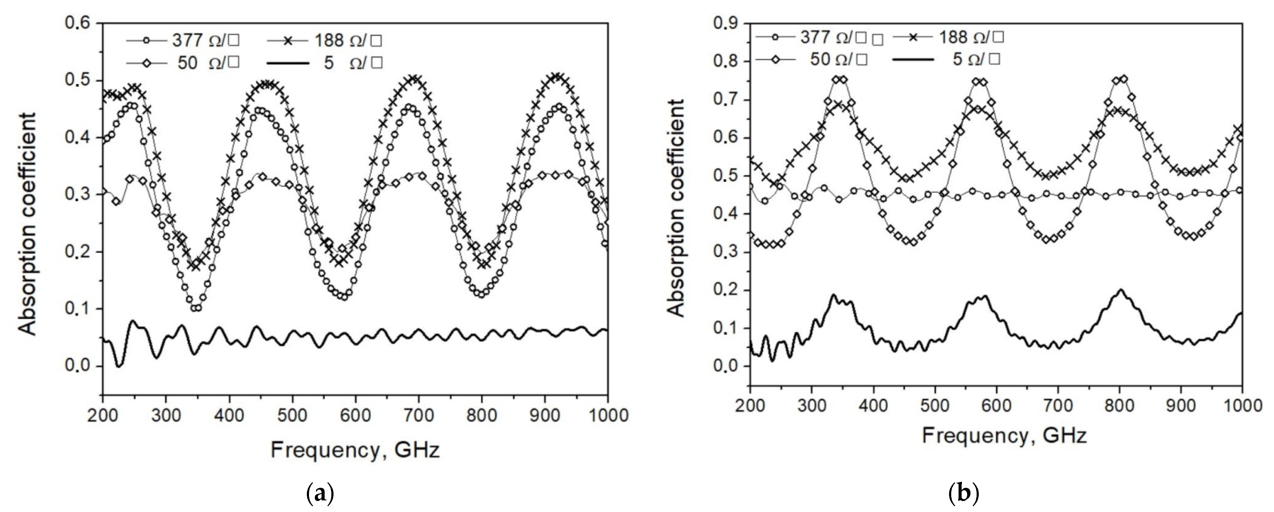
Figure 1. Modeled absorption coefficient for films with different resistance values (Ω/□): (a) irradiation from film side; (b) irradiation from substrate side.
The bare dielectric substrate with refractive index n at both sides should have a reflection coefficient R = [(n − 1)/(n + 1)]2, so for silicon with n = 3.4, R = 0.3. Antireflection coating with electrical thickness of one-quarter wavelength and refractive index na = n0.5 can be used to decrease reflections in the relatively narrow band. The modeled absorption coefficients of film with resistance of 188 Ω/□ on different 340 μm substrates (sapphire, quartz, silicon) and on substrate with additional antireflective coating are presented in Figure 2.
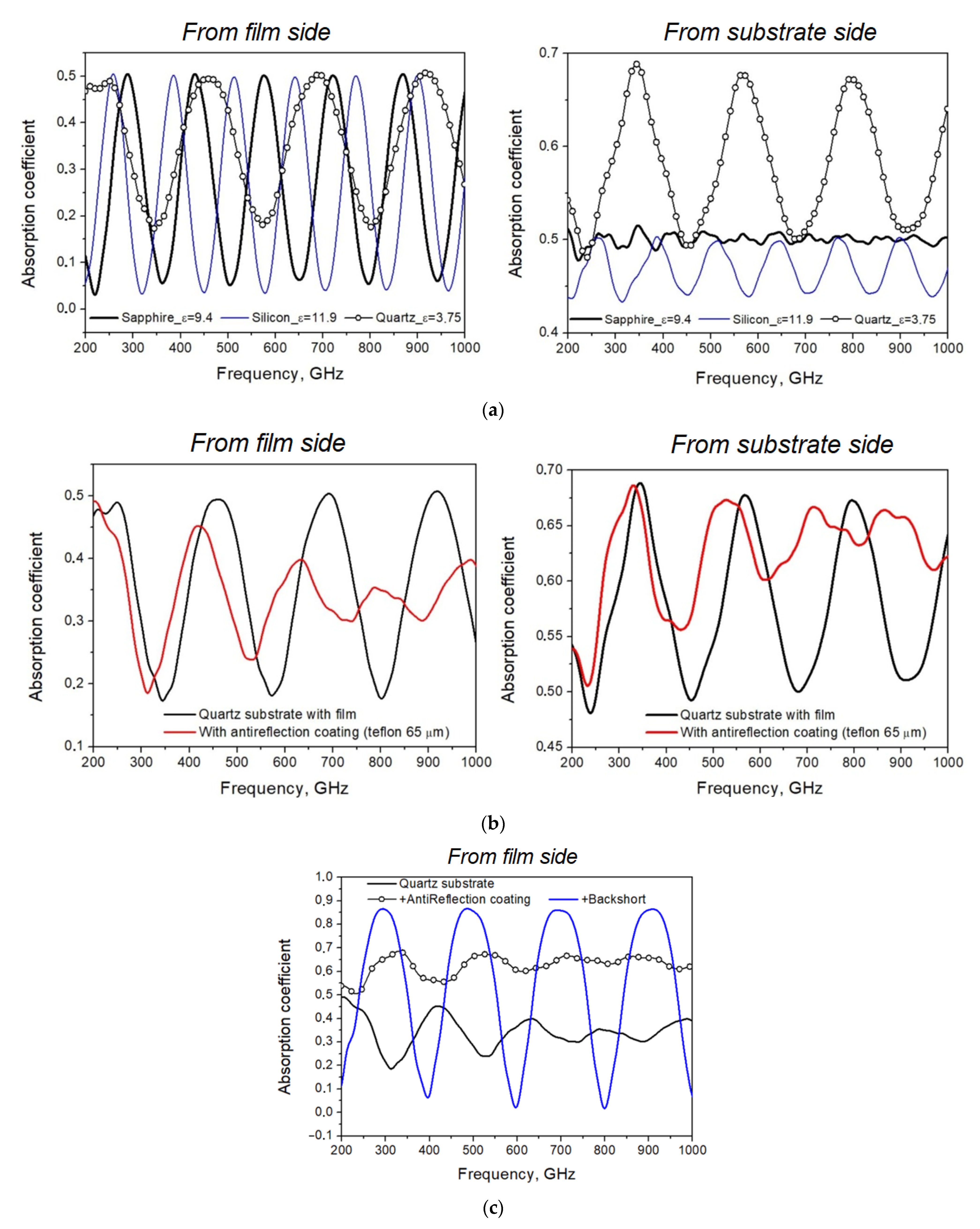
Figure 2. Modeled absorption coefficient of film with resistance of 188 Ω/□ on different substrates: (a) sapphire, silicon and quartz 340 μm substrates, irradiation of film side (left) and substrate side (right); (b) quartz 340 μm substrate with antireflection coating made of 65 μm-thick Teflon, irradiation from film side (left) and substrate side (right); (c) comparison of results of modeling absorption coefficient of thin film on quartz substrate without and with antireflection coating and with additional backshort behind antireflection coating.
When using a substrate of finite thickness, the absorption spectrum becomes more complex because the periodic spectrum of the Fabry–Perot dielectric resonator is superimposed on the smooth dependence. This dependency is shown for the case of a resistive thin film with resistance per square of 30–300 Ω/□, which is too thin compared to the skin depth. So, for NiCr film with resistivity ρ = 10−6 Ωm, the resistance per square is 180 Ω/□ if the film thickness is 6 nm, but the skin depth of such film at f = 100 GHz is Δ = 503(ρ/f)0.5 = 1.5 μm. This means that more than 90% of power is transmitted through the substrate (see Figure 3).
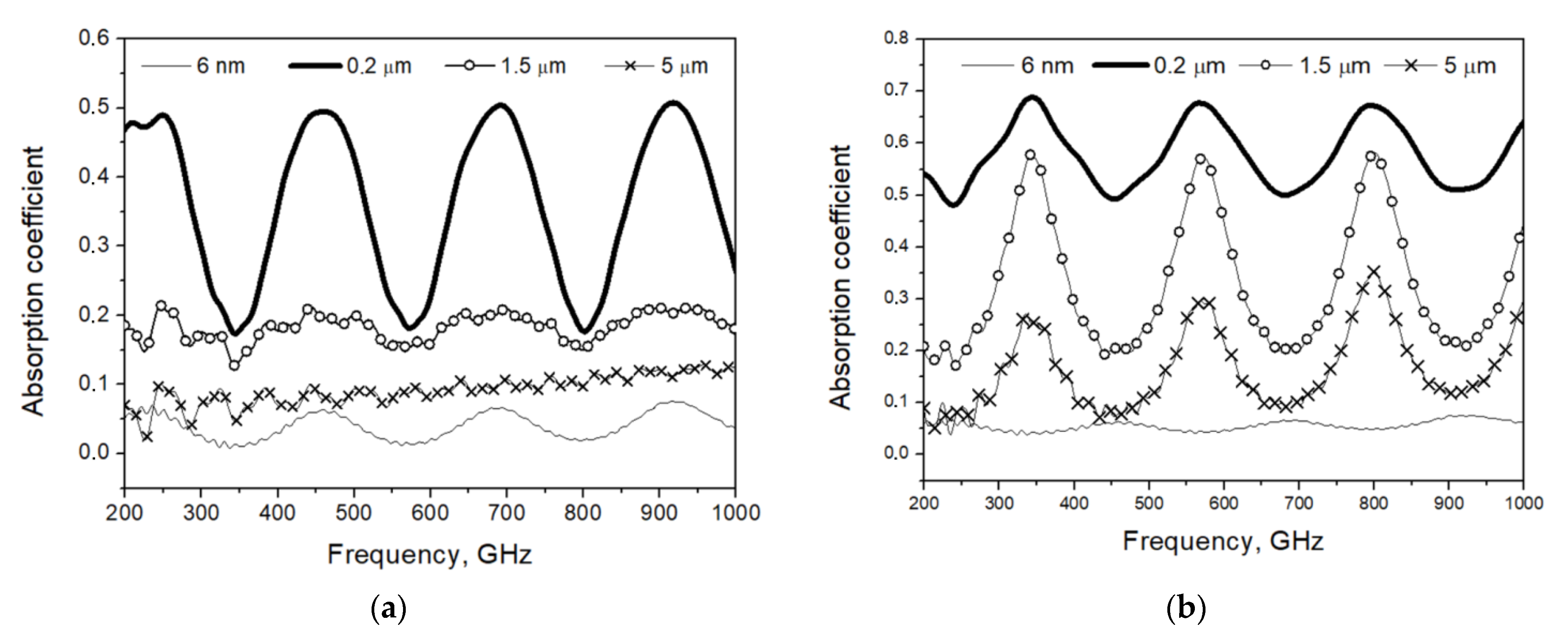
Figure 3. Calculated absorption coefficient of films with different thickness. Irradiation from (a) film side and (b) substrate side.
To increase the emissivity of a flat BB absorber, it is favorable to use relatively thick free-standing foil instead of an absorber comprising thin film on a dielectric substrate. For constantan with resistivity of 0.5 μΩ m at a signal frequency of 350 GHz, the skin depth is 0.6 μm, so 50 μm-thick foil is definitely opaque. In [7], 50 μm constantan foil was mounted (glued by black thermally conductive STYCAST epoxy on copper foil to equalize the temperature) at a temperature stage of 0.4 K. On the reverse side, two resistors were glued to the copper carrier, one to measure the temperature and one for heating, and a miniature permanent magnet was mounted on this rotatable holder. The reflectance coefficient of the foil at a frequency of 350 GHz was measured by a BWO spectrometer/reflectometer; it was 0.7 ± 0.05, meaning that the blackness was k = 0.3 ± 0.05. Since such a source has high inertia, cold aperture switching was used for remote switching from cold to hot load by the external permanent magnet [8][9]. The whole assembly, which is fixed on an axle, can be rotated by the external magnet, and in this way, the hot or cold emitter appears in the aperture of the immersion lens. A demonstration of the room-temperature model of rotating cryogenic absorber and reflector is presented in Figure 4.
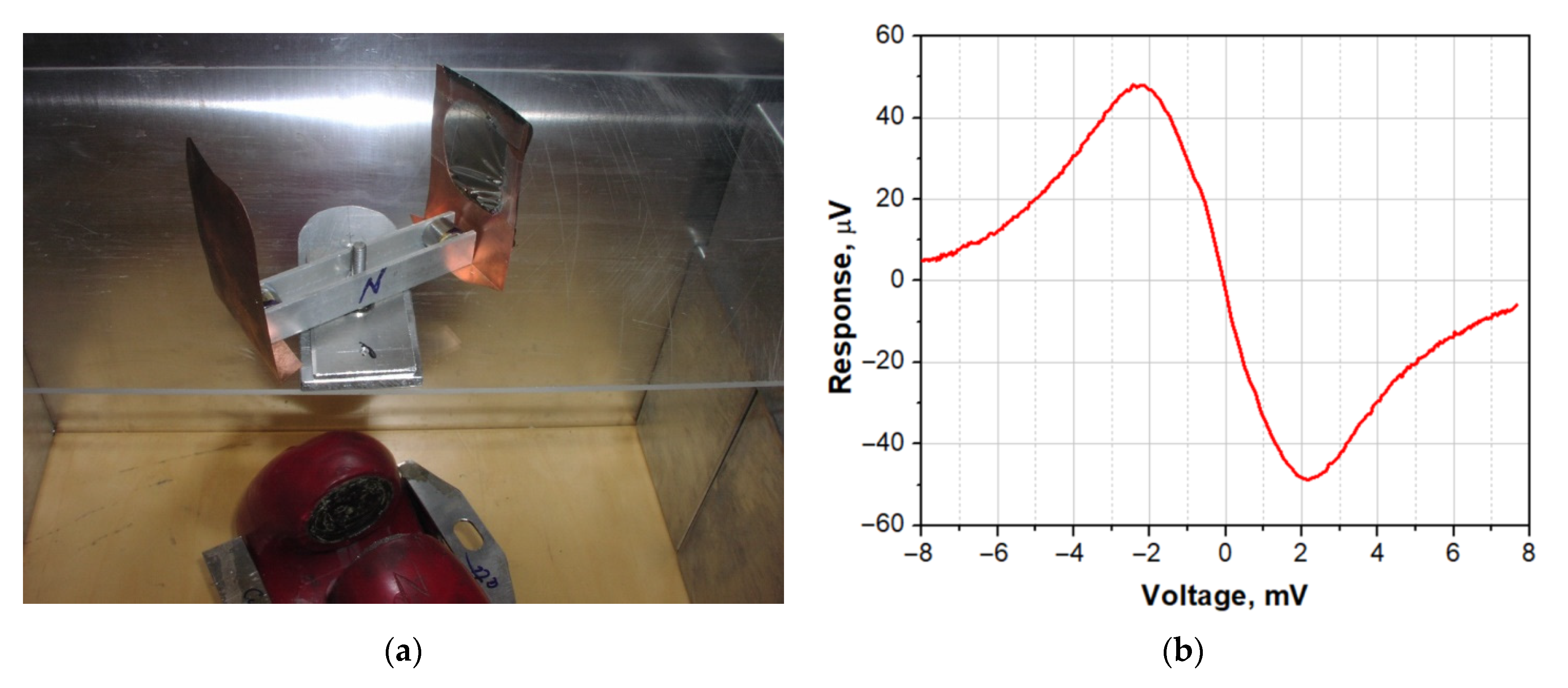
Figure 4. (a) Room-temperature demonstration model of rotating cryogenic absorber and reflector and (b) measured voltage response of SINIS detector to switching of aperture from reflector to thin film 10 dB absorber made on Kapton.
Using an integrating cavity in which the radiation is multiply reflected from the walls, accompanied by absorption in the semi-transparent film, can be a more effective method for increasing the absorption. Examples of devices with integrating cavities are shown in Figure 5
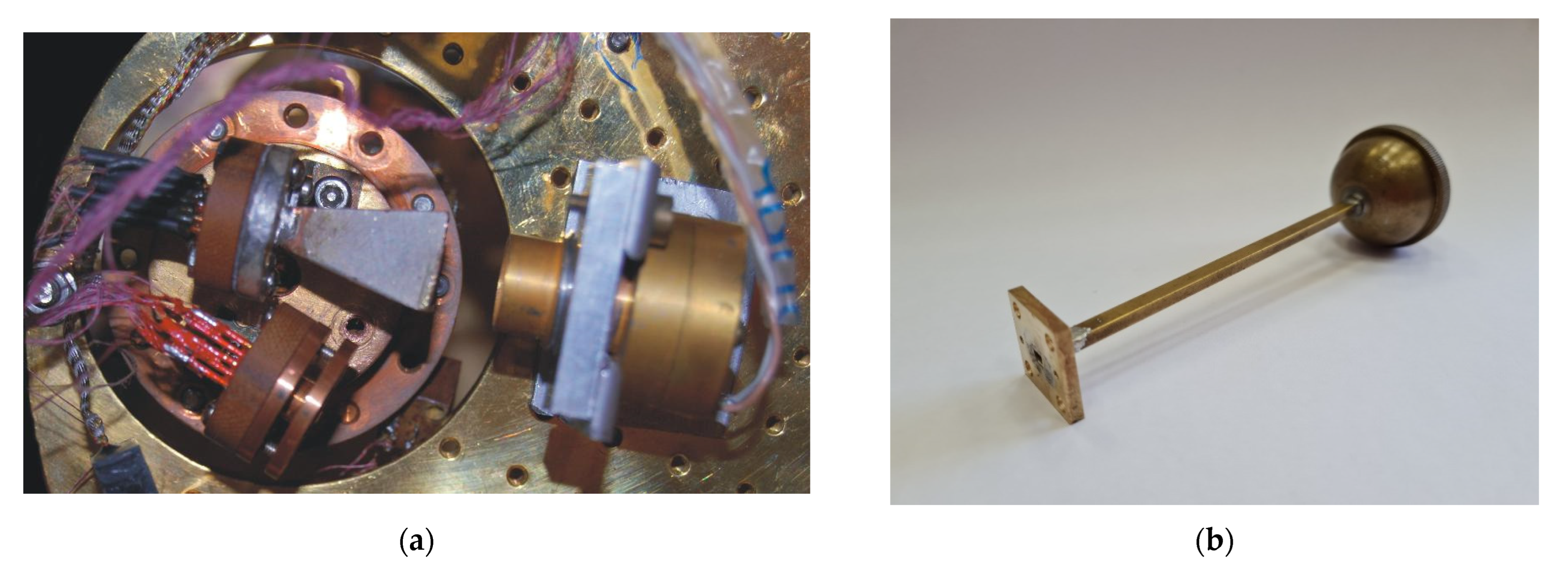
Figure 5. (a) Integrating cavity with NiCr film on sapphire substrate at 2.8 K stage in cryostat with the sample (left) at 280 mK stage; (b) photo of spherical integrating cavity for measurements with P2-69 SWR meter.
A series of samples on silicon substrate (24 × 5 × 0.5 mm) with different thicknesses of NiCr thin film was made to investigate the influence of film resistance and location on the efficiency of integrating cavity. The samples were mounted inside a spherical copper integrating cavity 33 mm in diameter with a 3.6 × 1.8 mm waveguide port, Figure 5b. The sample with thin film was glued at an angle of 10° in the middle of the sample holder. The reflectance coefficient was measured using a P2-69 reflection and transmission spectrometer in the frequency range of 52–80 GHz. At a frequency of 70 GHz for film with 100 Ω/□ resistance, the reflectance coefficient was −6.5 dB, indicating that the blackness was about 80%.
To increase scattering in the integrating cavity, the second type of sample was deposited on unpolished Si substrate 32 mm in diameter, which completely filled the middle of the cavity (a photo of the film surface and its profile are shown in Figure 6). In this case, the blackness was more than 85%. The roughness of the surface was more than 1 μm, and resistance of NiCr thin film was 200 Ω/□, in contrast to the film on polished substrate (20 Ω/□), which was deposited by the same process as the film on unpolished substrate. The calculated dependence of effective conductivity on frequency for film roughness of 2.5 μm is presented in Figure 7a, and a comparison of absorption coefficients for perfect (with negligible roughness and fixed conductivity) and “real” substrate is presented in Figure 7b.
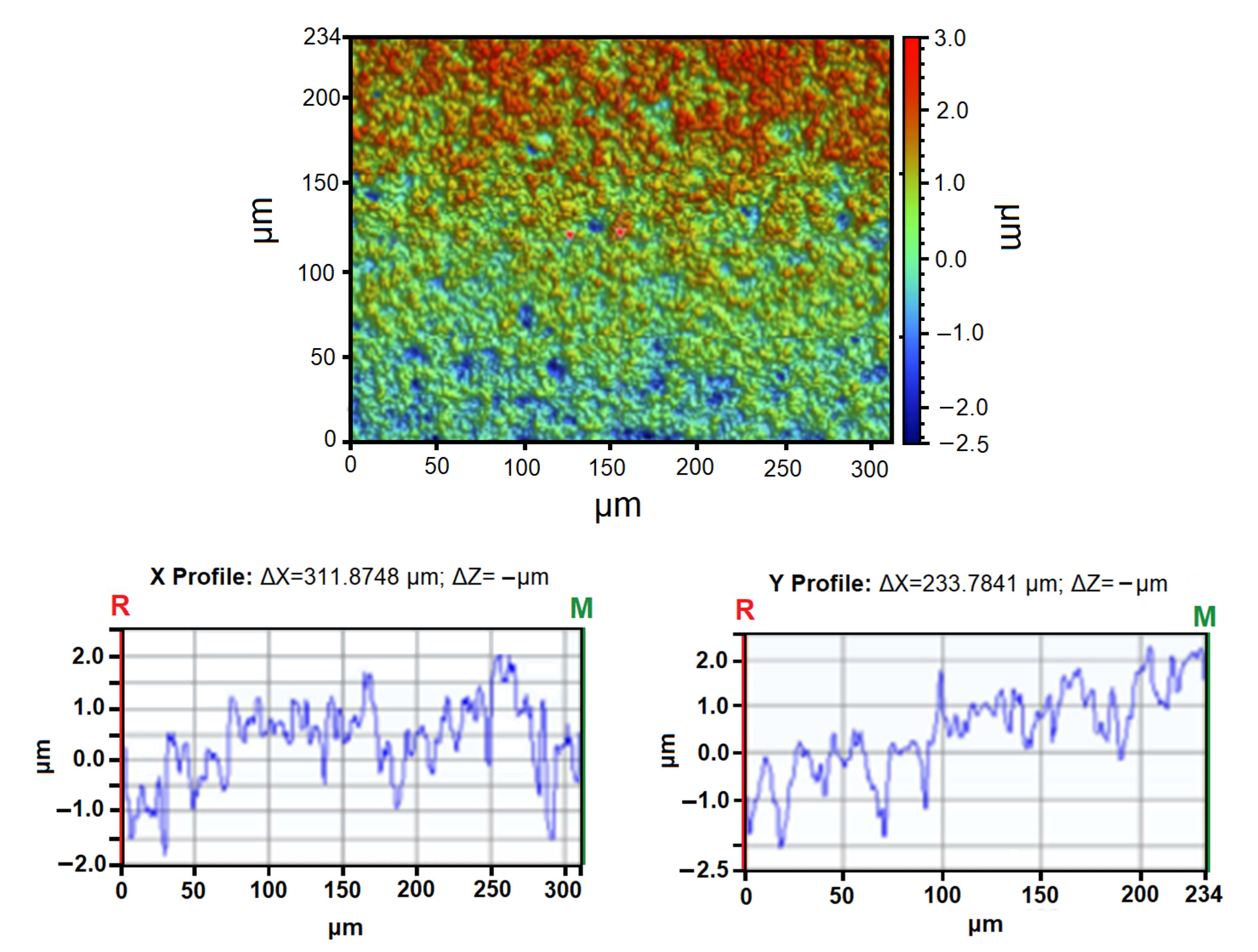
Figure 6. Images of rough silicon substrate with deposited NiCr 280 nm film.
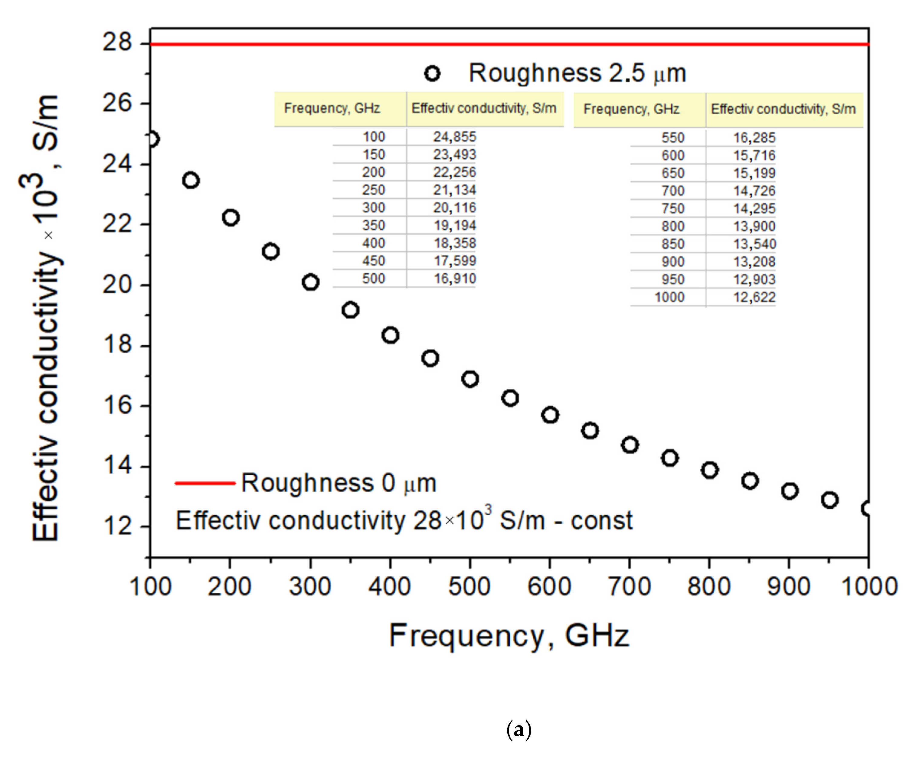
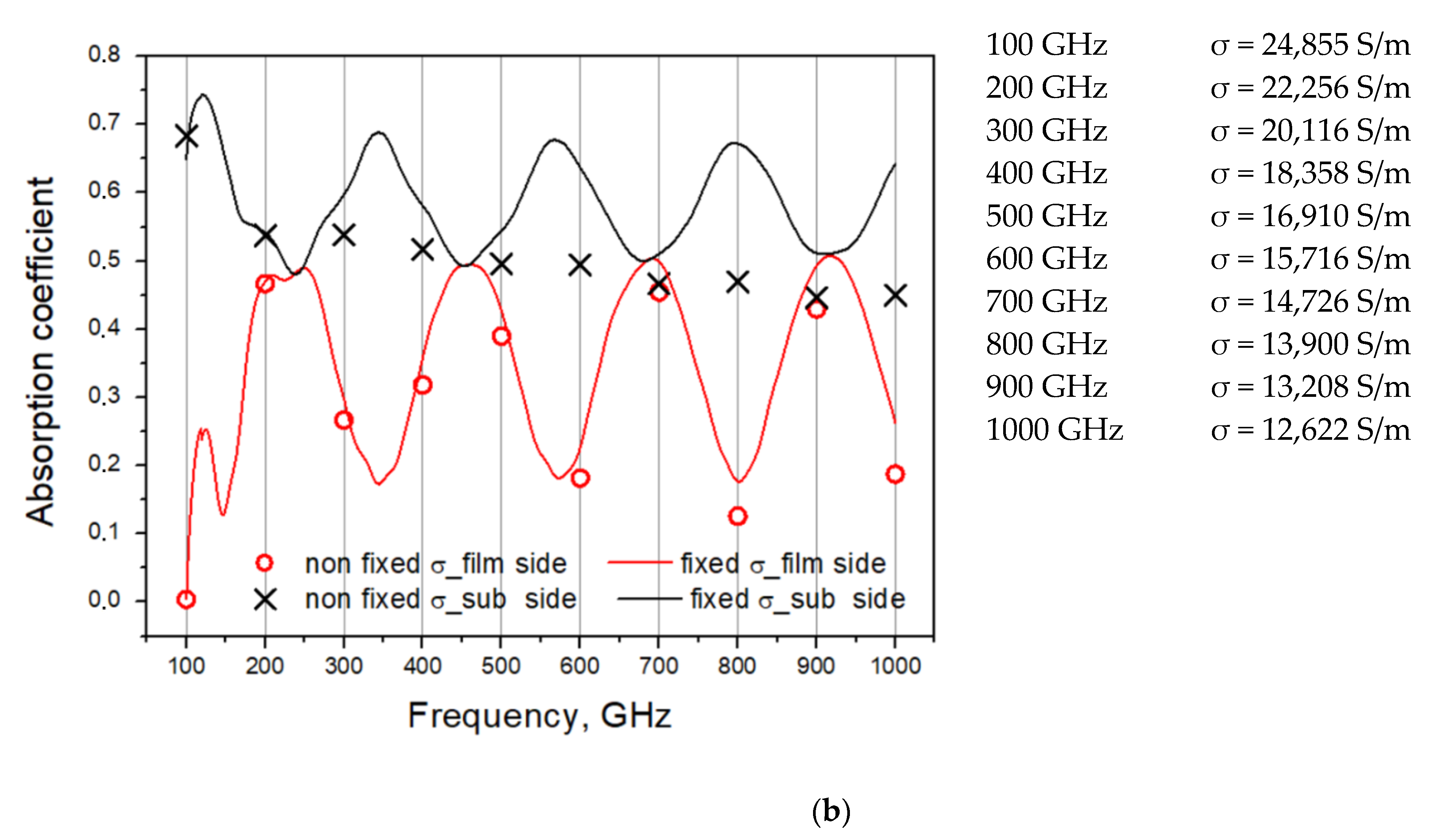
Figure 7. Calculated dependence of film characteristics on surface roughness: (a) dependence of effective conductivity on frequency for film with roughness of 2.5 μm; (b) absorbance coefficient of thin film at different frequencies depending on value of effective conductivity.
References
- Persky, M.J. Review of black surfaces for space-borne. Rev. Sci. Instrum. 1999, 70, 2193–2217
- Surrey Nanosystems. Vantablack Coating Technology. Available online: https://www.surreynanosystems.com (accessed on 31 May 2022)
- Hargravea, P.; Wasketta, T.; Limb, T.; Swinyardb, B. Performance of flight-model on-board calibration sources on Herschel-SPIRE. In Proceedings of the SPIE Astronomical Telescopes + Instrumentation, Orlando, FL, USA, 24–31 May 2006; Volume 6275.
- Pisano, G.; Hargrave, P.; Griffin, M.; Collins, P.; Beeman, J.; Hermoso, R. Thermal illuminators for far-infrared and submillimeter astronomical instruments. Appl. Opt. 2005, 44, 3208–3217.
- Parmar, N.; Sinha, A.; Pathak, S.K.; Kshatriya, A.J. Design and simulation of high temperature black body source for calibration of Michelson interferometer ECE diagnostic. Fusion Eng. Design 2021, 172, 112752.
- Lemzyakov, S.A. Interaction of Submillimeter Wave Radiation with SINIS Structures. Ph.D. Thesis, P. Kapitza Institute for Physical Problems, Moscow, Russia, 2021.
- Tarasov, M.; Kuzmin, L.; Edelman, V.; Kaurova, N.; Fominsky, M.; Ermakov, A. Optical response of a cold-electron bolometer array. JETP Lett. 2010, 92, 416–420.
- Tarasov, M.A.; Kuzmin, L.S.; Kaurova, N.S.; Otto, E.A.; Yassin, G.; de Bernardis, P. Cold-electron bolometer array integrated with a 350 GHz cross-slot antenna. In Proceedings of the 21 International Symposium on Space Terahertz Technology, Oxford, UK, 23–25 March 2010; pp. 256–261.
- Tarasov, M.; Kuzmin, L.; Edelman, V.; Mahashabde, S.; de Bernardis, P. Optical response of a cold-electron bolometer array integrated in a 345 GHz cross-slot antenna. IEEE Trans. Appl. Supercond. 2011, 21, 3635–3639.
More
Information
Subjects:
Physics, Applied
Contributors
MDPI registered users' name will be linked to their SciProfiles pages. To register with us, please refer to https://encyclopedia.pub/register
:
View Times:
1.1K
Revisions:
4 times
(View History)
Update Date:
28 Jul 2022
Table of Contents


Notice
You are not a member of the advisory board for this topic. If you want to update advisory board member profile, please contact office@encyclopedia.pub.
OK
Confirm
Only members of the Encyclopedia advisory board for this topic are allowed to note entries. Would you like to become an advisory board member of the Encyclopedia?
Yes
No
${ textCharacter }/${ maxCharacter }
Submit
Cancel
Back
Comments
${ item }
|
${ item.createdUser.fullName }
${ item.createdAt }
${ item.vote }
${ item.reply }
Delete
${ reply.createdUser.fullName }
${ reply.createdAt }
${ reply.vote }
Delete
There is no reply to this comment~
${ item.replyTextCharacter }/${ item.replyMaxCharacter }
Submit
Cancel
More
No more~
There is no comment~
${ textCharacter }/${ maxCharacter }
Submit
Cancel
${ selectedItem.replyTextCharacter }/${ selectedItem.replyMaxCharacter }
Submit
Cancel
Confirm
Are you sure to Delete?
Yes
No