Your browser does not fully support modern features. Please upgrade for a smoother experience.
Submitted Successfully!
 +1 credit
Thank you for your contribution! You can also upload a video entry or images related to this topic.
For video creation, please contact our Academic Video Service.
| Version | Summary | Created by | Modification | Content Size | Created at | Operation |
|---|---|---|---|---|---|---|
| 1 | Huachao Zai | -- | 3348 | 2022-07-06 16:01:40 | | | |
| 2 | Beatrix Zheng | + 1 word(s) | 3349 | 2022-07-07 04:34:14 | | |
Video Upload Options
We provide professional Academic Video Service to translate complex research into visually appealing presentations. Would you like to try it?
Cite
If you have any further questions, please contact Encyclopedia Editorial Office.
Wang, L.; Liu, G.; Xi, X.; Yang, G.; Hu, L.; Zhu, B.; He, Y.; Liu, Y.; Qian, H.; Zhang, S.; et al. Annealing Methods in the Growth of Perovskite Grains. Encyclopedia. Available online: https://encyclopedia.pub/entry/24871 (accessed on 25 June 2026).
Wang L, Liu G, Xi X, Yang G, Hu L, Zhu B, et al. Annealing Methods in the Growth of Perovskite Grains. Encyclopedia. Available at: https://encyclopedia.pub/entry/24871. Accessed June 25, 2026.
Wang, Lan, Guilin Liu, Xi Xi, Guofeng Yang, Lifa Hu, Bingjie Zhu, Yifeng He, Yushen Liu, Hongqiang Qian, Shude Zhang, et al. "Annealing Methods in the Growth of Perovskite Grains" Encyclopedia, https://encyclopedia.pub/entry/24871 (accessed June 25, 2026).
Wang, L., Liu, G., Xi, X., Yang, G., Hu, L., Zhu, B., He, Y., Liu, Y., Qian, H., Zhang, S., & Zai, H. (2022, July 06). Annealing Methods in the Growth of Perovskite Grains. In Encyclopedia. https://encyclopedia.pub/entry/24871
Wang, Lan, et al. "Annealing Methods in the Growth of Perovskite Grains." Encyclopedia. Web. 06 July, 2022.
Copy Citation
Perovskite solar cells (PSCs) are a promising and fast-growing type of photovoltaic cell due to their low cost and high conversion efficiency. The high efficiency of PSCs is closely related to the quality of the photosensitive layer, and the high-quality light absorbing layer depends on the growth condition of the crystals. In the formation of high-quality crystals, annealing is an indispensable and crucial part, which serves to evaporate the solvent and drive the crystallization of the film. Various annealing methods have different effects on the promotion of the film growth process owing to the way they work.
perovskite solar cells
annealing
perovskite crystallization
driving force
1. Physical Annealing
Physical annealing primarily uses electromagnetic waves, thermal energy, ultrasonics, pressure and other physical strategies to promote precursor reactions and crystallization of perovskite [1][2][3]. Physical annealing is mostly non-direct contact annealing, which reduces the possibility of introducing impurities. This method is also environmentally friendly, which is a suitable annealing strategy for future commercial fabrication.
1.1. Thermal Annealing
Direct thermal annealing of the substrate after spin-coating the precursor solution is the extensive method used by numerous researchers to crystallize perovskite as its convenience and simplicity [1][4][5]. During thermal treatment, the researcher found there was an annealing window, which would strongly enhance the crystallinity of perovskite film. The choice of thermal annealing window in crystallization was significant for the growth of the crystals [6][7][8]. The mixed halide perovskites (Csx(FA0.83MA0.17)1−xPb(I0.83Br0.17)3) had three stages during the film growth process, which contained different crystal phases (Figure 1) [7].
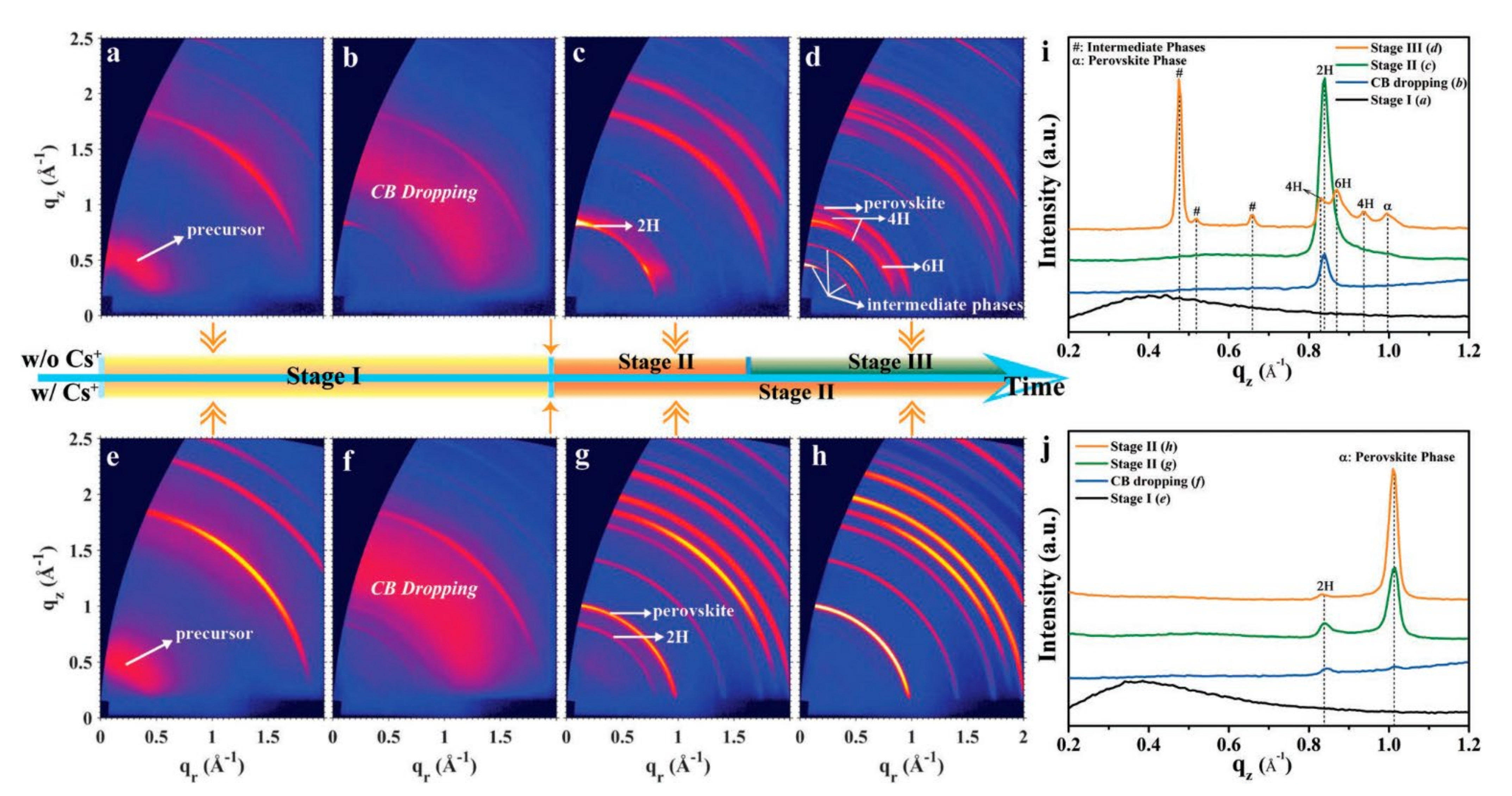
Figure 1. Different crystallization stages versus spinning time for perovskite formations without and with Cs+ (a–d); 2D GIWAXS patterns at different crystallization stages for films without Cs+ and with 10% Cs+ (e–h); (i,j) the intensity profiles along the qz direction for films without Cs+ (i) and with 10% Cs+ (j). Reprinted with permission from Ref. [7]. Copyright 2019 John Wiley & Sons.
Stage I was the precursor solution period; stage II was the main δ-phase (2H); and stage III contained the multiple complex phases, including two hexagonal polytypes (4H, 6H), CH3NH3I (MAI)–PbI2–Dimethyl sulfoxide (DMSO) intermediate phases and the α-phase. The crystalline phase of the perovskite showed stronger diffraction intensities and orientations when annealing at stage II, suggesting an internally stable and symmetrical structure. Actually, choosing to anneal within the annealing window could avoid the formation of hexagonal polytypes during the perovskite crystallization process. Furthermore, the annealing window can be extended by additional ions [6]. The time and temperature of the thermal annealing determines the quality of the crystals. The results of Huang et al. showed that the initial phase formed at 105 °C for 10 min, and the crystallinity and grain size continued to increase after 2 h of annealing [4]. However, prolonged thermal annealing may lead to decomposition of the film and device stability due to the fragility of the perovskite structure [9]. Some researchers have used high temperature rapid crystallization to solve the problem of long annealing times [1][10][11]. Annealing at high temperatures in a short time could induce the removal of solvent to build a supersaturation condition, which would accelerate the perovskite nucleation and improve the density of the nucleus [1]. Wei et al. demonstrated that annealing temperature played a key role in controlling the coarsening of the perovskite grains. The grain boundary was almost perpendicular to the substrate as the film was treated at 250 °C for 10 s.
Annealing at 400 °C for 4 s could also acquire a grain size of 1 μm [10], which improved the carrier transport properties. This instantaneous annealing of crystallization was attractive for industrial production, but it may come at the expense of some crystal quality. In fact, the fast evaporation rate of organic solvents led to the dramatic shrinkage of the grains. In addition, perovskite appeared turbid in scattered light due to the rough film, which was worse at higher temperatures [12]. Annealing immediately after spin-coating the precursor solution causes rapid volume shrinkage and the solute does not have enough time to diffuse, causing the rough surfaces and continuous cracking at grain boundaries.
Therefore, considering the fact that a slower evaporation rate could both reduce the crystallization rate and improve the quality of the crystals [5], gradient thermal annealing has been found to be an effective way to reduce the evaporation rate of organic reagents and slow down the crystallization process of films [5][13][14][15][16][17].
1.2. Electromagnetic Wave Annealing
Electromagnetic waves can radiate energy which have been used in many fields for heating, information transmission, etc. [18][19][20]. In the fabrication of perovskite, the main electromagnetic waves that have been used in the perovskite annealing process are infrared light waves, visible light, lasers and microwaves [3][21][22]. The intense pulsed light is a non-contact rapid heating method which can offer fast millisecond pulses of broad spectrum light (190–1100 nm) from xenon lamps [23]. Xenon lamps are used to provide high-energy pulse light to 150 J/cm2 for perovskite annealing, and can achieve thin film crystallization at the millisecond scale [5][19][24][25][26][27][28]. Druffel et al. successfully employed intense pulsed light generated by a xenon lamp to sintering of MAPbI3 on a mesoporous TiO2 substrate for first time [25]. The perovskites were subjected to 2000 J of energy in 2 ms. The films reached temperatures of 350–425 °C during the short-term heating and cooled to 100 °C within 3 ms, as the simulations displayed [29]. The extremely short times may result in the incomplete growth of the film surface, and the conversion of perovskite at the millisecond level was still lower than that of thermal treatment. In actual fact, studies showed that appropriately extending the pulse time to increase grain growth time under intense light could lead to better film coverage and higher performance devices [27]. The addition of light-absorbing material can improve the reaction rate of perovskite. The diiodomethane (CH2I2) additive can also improve surface coverage during rapid crystallization and enhance carrier transport [19]. The intense pulse annealing with halogen lamps was compatible with roll-to-roll manufacturing, which enabled production speeds of 26 m/min [26].
In the fabrication of perovskite films, infrared light can effectively promote precursor reactions and drive grain growth [21][29][30][31][32][33][34][35][36][37][38][39]. Infrared light is an electromagnetic wave with a frequency between microwave and visible light. The application of infrared light for annealing treatments mainly utilizes its ability to provide a large amount of energy in a short amount of time [32][33].
Providing a large amount of energy in a short time to achieve rapid annealing has potential for future industrial production. However, according to the principles of crystal crystallization, the fast crystallization rate resulted in a poorer crystal quality and may also introduce greater stresses, leading to problems in the subsequent stable operation of the device [5].
Lasers can provide a great strategy for modulating the crystallinity and electrical properties of films due to their high energy and excellent monochromatic characteristics, and are widely used in the fabrication of perovskite layers, such as the electron transport layer TiO2, the hole transport layer NiO, and the electrodes [22][40][41][42]. Lasers also perform well in the promotion of crystallization of the functional layers [43][44][45][46][47][48][49]. Compared to the pulsed light annealing discussed above, the laser had a remarkable ability to promote crystallization, and the efficiency of the device exceeded 20% [43]. The laser spot was scanned at a speed under the control of the program that produced a maximum temperature of 100 °C on the film surface. Results from other researchers’ simulations also showed that the laser can generate temperatures of over 100 °C inside the film [44]. The films had superior crystallinity and orientation in the laser-driven mode. In addition, different wavelengths of laser light had different impacts on the growth of the films. The grains had a better grain size at 450 nm, probably due to the high absorption of perovskite at short wavelengths in the non-UV. The researchers believed that the localized temperature gradient created by the laser at the perovskite grain boundaries would allow larger grains to absorb more energy and have higher temperatures than smaller grains, thus inducing selective growth of larger grains. The energy received by the film per unit time was related to the out-of-focus distance of the laser and the scanning speed, which would affect the properties of the crystal. The band gap narrowed under laser annealing and the PL peak was red-shifted [48]. In the laser approach, there is an inverse relationship between the scan speed and energy density. After receiving higher energy density in the low-speed mode of laser crystallization, the interaction between the organic cation and the inorganic frameworks of the film was enhanced, which resulted in the right shift in the conduction bands (CB) and valence bands (VB). The research also found that the conductivity of the perovskite surface would convert from P-type to N-type as the scan speed changed from high to low, which might be due to an increase in the conversion of perovskite. The laser annealing had a significant effect on stresses in thin film growth, where it can reduce tensile stresses during growth [46][48]. Regular thermal treatments will generate high tensile stresses within the film [50][51], causing perovskite to decompose, and promoting the formation of numerous defects, which adversely affected the carrier transport of defect trapping. The reduction in stress release comes from the fact that the laser enhanced ultrafast diffusion in the perovskite films. The 40% stress was reduced in the film by the laser, and the degradation rate of the film was cut down by more than two times at 80% humidity [46]. Laser annealing was equally applicable to flexible polymer substrates, which protected other functional layers from damage in the fabrication of flexible PSCs [44]. In addition, the compatibility between the different transport layers and the laser annealed film should also be taken into account for improving the device efficiency [45].
UV has been considered detrimental to perovskite films due to its ability to break down the active components within the perovskite [52][53]. However, utilizing the high absorption of perovskite in the UV band appropriately can promote crystallization. Li et al. applied a 365 nm UV light emitting diode (LED) to achieve the accurate annealing of the perovskite layer by controlled UV light irradiation [54], which significantly eliminated the hysteresis effect and obtained a device with an efficiency of 19%. UV light can be annealed by controlling the amount of irradiation. Therefore, it's suggested that the wavelengths in the various types of light annealing might be extended to the UV band to improve energy utilization rate and reduce the consumption.
Microwaves are part of the electromagnetic wave, with a wavelength ranging from 1 m to 1 mm, which commonly converts energy from electromagnetic energy to thermal energy rather than heat transfer [55][56][57]. Several studies have demonstrated that microwaves also convey excellent control of perovskite crystallization [58][59][60][61].
However, there was no definitive conclusion on the growth mechanism of perovskite under microwaves. Mascarenhas concluded that microwaves made the internal polar solvent N,N-Dimethylformamide (DMF) and DMSO dipole vibrate at high frequencies, and then generated heat to crystallize the perovskite film rapidly [60]. This was supported by the phenomenon that only the perovskite powders that contained DMF or DMSO solvents turned black under microwave irradiation [62]. Other studies attributed the crystallization effect to the absorption of microwaves by the substrate, which drove the crystallization of the film [58]. A third explanation has suggested that the dipolar polarization and conductive mechanisms worked together, and were responsible for the controllable crystallization of perovskites films [60].
1.3. Ultrasonic Annealing
Ultrasonically induced crystallization is also an alternative to heat treatment as an annealing method. Eslamian et al. used ultrasound to induce crystallization for 3 min after spin-coating the precursor solution, and obtained an efficiency of 14.09% [63]. Zhang et al. prepared the device with an efficiency of over 17% at room temperature by using ultrasound at 40 kHz [64]. Ultrasonically induced growth is cold processing, which is a viable crystallization method for the processing of flexible cells. Due to the simplicity of ultrasonic equipment, ultrasonics can be used in subsequent large area preparation processes such as spraying, blade and slot die coating processes.
1.4. Pressure Annealing
Pressure is a universal and controllable thermodynamic variable that can be used to alter the electronic structure and properties of materials [65][66][67][68]. In the growth of perovskite, the addition of pressure could achieve regulation of film crystallization, which can obviously improve the grain size of perovskite, crystallinity, stability under humidity, and defect density [69][70][71][72]. The role of pressure in perovskite crystallization was mainly employed to regulate the evaporation and sublimation of volatiles, and thus improve the quality of crystals [2].
2. Chemical Annealing
The researchers have defined chemical annealing as the addition of chemicals to assist crystallization during the annealing of perovskite or using chemical reagents to directly complete crystallization without thermal treatment. For example, the chemical reagents have been combined with traditional thermal treatments to improve the crystalline quality of the film by dissolving–recrystallizing the perovskite film, or reducing the evaporation of organic solvents [73][74]. On the other hand, researchers have used the principle of extracting polar solvents with organic reagents to achieve the supersaturated crystallization of perovskite, or have added ions into the precursor liquid to complete the coating and crystallization of the film at the same time [75][76].
2.1. Solvent Annealing
Solvent annealing for crystalline modulation is achieved by the addition of polar solvent vapor to the annealing [77][78][79][80][81][82][83][84]. Solvent annealing (SA) was first introduced to the perovskite crystallization by Huang et al. [85]. The organic polar solvent vapor provided a humid environment, and the high solubility of PbI2 and MAI in DMF vapor resulted in longer diffusion distances for precursor ions and molecules than in thermal annealing (TA), which promoted grain growth and produced larger grain sizes.
SA could form almost defect-free perovskite crystallites [86]. The electrical properties within the grain plane of the recrystallized grains were superior to grain boundaries within the grain plane. The conductive atomic force microscopy (c-AFM) results revealed that the peak current values for representative grains in SA (17 nA) were higher than those in TA (16 nA), indicating that the in-plane electrical properties of grains under recrystallization in a solvent atmosphere were superior to the grain boundaries [87]. The DMF solvent-annealed perovskite films also displayed a more prominent carrier recombination effect in the grain boundaries, which might account for the greater improvement in photoconductivity in the grain plane than in the boundaries in solvent annealing [88]. The concentration of DMF vapor needed to be reasonably controlled, as the excessive DMF vapor was a challenge to the photovoltaic performance of the film [89]. DMF and DMSO have already become the most widely considered choices in many solvents due to their significant dissolution–recrystallization effects and their ease of removal from perovskite films [73][79][81][87][88][89][90][91][92]. DMSO solvent annealing also had an excellent ability to form grains with low defect density. However, unlike DMF annealing, the DMSO-treated films showed a blue-shift in the photoluminescence peak; some studies attributed this phenomenon to an increase in band gap during the annealing process [93], while others suggested that the shift came from the relatively low trap density near the band edge [78]. The synergistic annealing of various solvents further improved the effect of single solvent annealing. A small amount DMSO added into DMF could regulate the growth by forming MAI-PbI2-DMSO intermediate phases with strong Lewis basicity, allowing extensive incorporation and the disappearance of grain boundaries [81]. Compared to single IPA or DMF annealing, mixed solvent annealing of DMF and IPA was superior in improving device stability and eliminating hysteresis effects [79]. In addition, DMF/DMSO mixed with chlorobenzene (CB), propanol, H2O, etc., were also applied to improve the crystalline quality [73][92]. Researchers have also developed some polar solvents to replace the organic solvents to achieve annealing, such as pyridine, CB, 1-Methyl-2-pyrrolidinone (NMP), etc. [94][95][96]. Alcohols such as methanol, ethanol, isopropanol, n-butanol and benzyl alcohol were applicable in solvent annealing engineering [97][98][99]. Alcohol annealing significantly suppressed the dark current and elevated the photocurrent, with methanol vapor becoming the most prominent in terms of high reproducibility and elimination of photocurrent hysteresis [97].
Methylamine-based chemical vapors also performed remarkably in inducing annealing in perovskite [100][101][102][103][104]. The methylamine vapors were annealed in the same solid–liquid–solid process as any other solvent annealing modes. In the fabrication of printable mesoscopic PSCs [101], methylamine improved the pore filling of perovskite in the mesoscopic structure, resulting in films with complete surface coverage and a high degree of crystallinity. The PbI2 would be distributed on the surface and grain boundaries of the film after methylamine vapor recrystallization, which passivated the internal defects. The addition of methylamine reduced the weave of the films with random grain orientations [100]. The backscattered electron (BSE) results of film revealed that the textured grains were well defined, with sizes ranging from 10 to 50 μm after methylamine annealing treatment, and the X-axis inverse pole figure showed that the grain orientation under methylamine gas annealing was mainly concentrated in the (1,0,1) (0,0,1) plane. This method could effectively induce the growth of highly oriented and full-coverage films; methylamine was intrinsic to perovskite and there was no possibility of introducing excess impurities during the annealing process. Not only organic solvents but also water was confirmed to achieve self-healing of grains in annealing [105][106][107][108][109]. Snaith et al. demonstrated that moisture could solvate the methylammonium component and “self-heal” the perovskite lattice [106]. The films that annealed at high humidity showed higher photoluminescence quantum efficiency and carrier life due to the reduced density of traps. Moisture dissolved hygroscopic organics (formamide, methylammonium and possibly other components) during the annealing process and allowed them to effectively repair the perovskite structural domains or boundaries [109], filling any trap states created during the manufacturing process.
2.2. Solvent–Solvent Extraction Annealing
Perovskite films are driven to crystallization by an oversaturated environment created by the reduction of solvent. The solvent evaporation is reduced by normal heating in perovskite films, which is not optimal for the fabrication of flexible cells. Therefore, through the principle of mutual solubility of organic solvents, some researchers have chosen specific organic reagents to extract the polar solvent inside the film to drive crystallization [110][111][112][113]. Ether-based chemical materials were the most commonly used extractants, which had the characteristics of low polarity, stable properties, being less likely to react with airborne components, and a low boiling point [106][108]. Padture et al. proposed the use of diethyl ether (C2H5OC2H5) for induced crystallization [114]. The substrates were immersed in a room temperature bath of solvent diethyl ether for two minutes immediately after spin-coating the MAPbI3 precursor. The films were dried at room temperature to produce smooth films with a PCE of up to 15.2%. An additional anti-solvent treatment prior to immersion in ether (DDE) successfully enhanced the crystallinity of the extractive annealing, resulting in the device efficiency of 19.5% [110]. Anisole solutions had the superior ability to drive crystallization [112].
2.3. Encapsulation Layer Annealing
The encapsulation layer annealing was performed by adding a layer on the surface of perovskite to form a sandwich structure with the upper and lower layers [76][115]. The existence of the encapsulated layer in the annealing process improved the film growth by retarding the evaporation of the solvent. The restrained solvent would induce the obvious dissolution–recrystallization process, which led to high quality films with large sized grains. Wei et al. introduced PC61BM as a barrier layer before annealing, which developed a sandwich structure of substrate/perovskite/PC61BM to retard the extravasation of solvent during annealing [115]. The escape of the residual solvent was prevented by the PC61BM, resulting in the dissolution of the grains. The recrystallized grains were coarsened, which improved the photovoltaic performance of PSCs.
2.4. No Annealing
The addition of specific reagents to the precursor solution enables the film to be directly transformed from liquid to solid during the spin-coating process, avoiding additional annealing treatments [74][116][117][118]. Chen et al. proposed a method for the preparation of annealing-free perovskite films by introducing guanidine iodide (GAI) [117]. The organic molecule guanidine (GA (+)) had a large ionic radius, which could control the crystallization rate of annealing-free films, and the films were characterized by low defect density and a large grain size. NMP was added to the dimethylacetamide (DMAc) precursor solution and would insert into the PbI2 lattice to produce an intermediate phase MAI-PbI2-NMP, which was similar to MAI-PbI2-DMSO [116]. The NMP was rapidly removed after dropping the antisolvent, completing the immediate nucleation and grain growth of the perovskite film. In addition, 2-Methoxyethanol (2-ME) and NH4Cl also displayed the ability to promote crystallization [74][118]. This crystallization mode had implications for the production of flexible cells, which eliminated pinholes and cracks generated by the thermal annealing process, while improving the reproducibility of the crystallization quality.
References
- Cao, X.B.; Zhi, L.L.; Jia, Y.; Li, Y.H.; Cui, X.; Zhao, K.; Ci, L.J.; Ding, K.X.; Wei, J.Q. High annealing temperature induced rapid grain coarsening for efficient perovskite solar cells. J. Colloid Interface Sci. 2018, 524, 483–489.
- Hua, J.C.; Deng, X.; Niu, C.; Huang, F.Z.; Peng, Y.; Li, W.N.; Ku, Z.L.; Cheng, Y.B. A pressure-assisted annealing method for high quality CsPbBr3 film deposited by sequential thermal evaporation. RSC Adv. 2020, 10, 8905–8909.
- Ghahremani, A.H.; Ratnayake, D.; Sherehiy, A.; Popa, D.O.; Druffel, T. Automated Fabrication of Perovskite Photovoltaics Using Inkjet Printing and Intense Pulse Light Annealing. Energy Technol. 2021, 9, 2100452.
- Bi, C.; Shao, Y.C.; Yuan, Y.B.; Xiao, Z.G.; Wang, C.G.; Gao, Y.L.; Huang, J.S. Understanding the formation and evolution of interdiffusion grown organolead halide perovskite thin films by thermal annealing. J. Mater. Chem. A 2014, 2, 18508–18514.
- Liu, C.; Cheng, Y.B.; Ge, Z.Y. Understanding of perovskite crystal growth and film formation in scalable deposition processes. Chem. Soc. Rev. 2020, 49, 1653–1687.
- Wang, S.B.; Chen, Y.Q.; Li, R.Y.; Xu, Y.B.; Feng, J.S.; Yang, D.; Yuan, N.Y.; Zhang, W.H.; Liu, S.; Ding, J.N. Superior Textured Film and Process Tolerance Enabled by Intermediate-State Engineering for High-Efficiency Perovskite Solar Cells. Adv. Sci. 2020, 7, 1903009.
- Qin, M.C.; Tse, K.F.; Lau, T.K.; Li, Y.H.; Su, C.J.; Yang, G.; Chen, J.H.; Zhu, J.Y.; Jeng, U.S.; Li, G.; et al. Manipulating the Mixed-Perovskite Crystallization Pathway Unveiled by In Situ GIWAXS. Adv. Mater. 2019, 31, 1901284.
- Kim, G.; Moon, C.S.; Yang, T.-Y.; Kim, Y.Y.; Chung, J.; Jung, E.H.; Shin, T.J.; Jeon, N.J.; Park, H.H.; Seo, J. A Thermally Induced Perovskite Crystal Control Strategy for Efficient and Photostable Wide-Bandgap Perovskite Solar Cells. Sol. RRL 2020, 4, 2000033.
- Van Franeker, J.J.; Hendriks, K.H.; Bruijnaers, B.J.; Verhoeven, M.; Wienk, M.M.; Janssen, R.A.J. Monitoring Thermal Annealing of Perovskite Solar Cells with In Situ Photoluminescence. Adv. Energy Mater. 2017, 7, 1601822.
- Kim, M.; Kim, G.H.; Oh, K.S.; Jo, Y.; Yoon, H.; Kim, K.H.; Lee, H.; Kim, J.Y.; Kim, D.S. High-Temperature-Short-Time Annealing Process for High-Performance Large-Area Perovskite Solar Cells. Acs Nano 2017, 11, 6057–6064.
- Shargaieva, O.; Lang, F.; Rappich, J.; Dittrich, T.; Kalus, M.; Meixner, M.; Genzel, C.; Nickel, N.H. Influence of the Grain Size on the Properties of CH3NH3PbI3 Thin Films. Acs Appl. Mater. Interfaces 2017, 9, 38428–38435.
- Lin, P.A.; Zhang, W.F.; Tian, L.W.; Zhang, F.; Zhou, S.H.; Liu, R.; Hu, T.T.; Zhang, M.; Du, L.; Wen, F.; et al. Remanent solvent management engineering of perovskite films for PEDOT: PSS-based inverted solar cells. Sol. Energy 2021, 216, 530–536.
- Huang, L.K.; Hu, Z.Y.; Xu, J.; Zhang, K.; Zhang, J.; Zhu, Y.J. Multi-step slow annealing perovskite films for high performance planar perovskite solar cells. Sol. Energy Mater. Sol. Cells 2015, 141, 377–382.
- Zhang, J.; Liang, W.S.; Yu, W.; Yu, S.W.; Wu, Y.L.; Guo, X.; Liu, S.Z.; Li, C. A Two-Stage Annealing Strategy for Crystallization Control of CH3NH3PbI3 Films toward Highly Reproducible Perovskite Solar Cells. Small 2018, 14, 1800181.
- Fan, B.B.; Peng, D.H.; Lin, S.W.; Wang, N.; Zhao, Y.; Sun, Y.M. Enhanced efficiency of planar-heterojunction perovskite solar cells through a thermal gradient annealing process. Rsc Adv. 2015, 5, 58041–58045.
- Xi, J.H.; Yuan, J.F.; Yan, X.Q.; Binks, D.; Tian, J.J. Gradient Annealing of Halide Perovskite Films for Improved Performance of Solar Cells. Acs Appl. Energy Mater. 2020, 3, 8130–8134.
- Xiao, Y.Y.; Meng, Y.Q.; Gao, H.L.; Chen, Y.C.; Meng, Q.; Bai, Y.J.; Wang, H.; Zhang, Y.Z.; Yan, H.; Han, C.B. Flexible perovskite solar cells fabricated by a gradient heat treatment process. Sustain. Energy Fuels 2020, 4, 824–831.
- Sadeghi, A.; Hassanzadeh, H.; Harding, T.G. Thermal analysis of high frequency electromagnetic heating of lossy porous media. Chem. Eng. Sci. 2017, 172, 13–22.
- Ankireddy, K.; Ghahremani, A.H.; Martin, B.; Gupta, G.; Druffel, T. Rapid thermal annealing of CH3NH3PbI3 perovskite thin films by intense pulsed light with aid of diiodomethane additive. J. Mater. Chem. A 2018, 6, 9378–9383.
- Nam, J.B.; Jang, Y.R.; Hwang, Y.T.; Kim, H.H.; Jung, I.H.; Kim, H.S. Intense Pulsed Light Sintering of Screen-Printed Paste Electrode on Silicon Solar Cell for High Throughput and Cost-Effective Low Temperature Metallization. Int. J. Precis. Eng. Manuf. -Green Technol. 2022, 9, 523–535.
- Sharma, B.; Singh, S.; Pareek, S.; Agasti, A.; Mallick, S.; Kabra, D.; Bhargava, P. Radiative and conductive thermal annealing of hybrid organic-inorganic perovskite layer. Sol. Energy Mater. Sol. Cells 2019, 195, 353–357.
- Girolami, M.; Bellucci, A.; Mastellone, M.; Serpente, V.; Orlando, S.; Valentini, V.; Palma, A.L.; Di Carlo, A.; Trucchi, D.M. Improving the Performance of Printable Carbon Electrodes by Femtosecond Laser Treatment. C-J. Carbon Res. 2020, 6, 48.
- Druffel, T.; Dharmadasa, R.; Lavery, B.W.; Ankireddy, K. Intense pulsed light processing for photovoltaic manufacturing. Sol. Energy Mater. Sol. Cells 2018, 174, 359–369.
- Ghahremani, A.H.; Pishgar, S.; Bahadur, J.; Druffel, T. Intense Pulse Light Annealing of Perovskite Photovoltaics Using Gradient Flashes. Acs Appl. Energy Mater. 2020, 3, 11641–11654.
- Lavery, B.W.; Kumari, S.; Konermann, H.; Draper, G.L.; Spurgeon, J.; Druffel, T. Intense Pulsed Light Sintering of CH3NH3PbI3 Solar Cells. Acs Appl. Mater. Interfaces 2016, 8, 8419–8426.
- Piper, R.T.; Daunis, T.B.; Xu, W.J.; Schroder, K.A.; Hsu, J.W.P. Photonic Curing of Nickel Oxide Transport Layer and Perovskite Active Layer for Flexible Perovskite Solar Cells: A Path Towards High-Throughput Manufacturing. Front. Energy Res. 2021, 9, 640960.
- Xu, W.J.; Daunis, T.B.; Piper, R.T.; Hsu, J.W.P. Effects of Photonic Curing Processing Conditions on MAPbI(3) Film Properties and Solar Cell Performance. Acs Appl. Energy Mater. 2020, 3, 8636–8645.
- Bahadur, J.; Ghahremani, A.H.; Gupta, S.; Druffel, T.; Sunkara, M.K.; Pal, K. Enhanced moisture stability of MAPbI(3) perovskite solar cells through Barium doping. Sol. Energy 2019, 190, 396–404.
- Muydinov, R.; Seeger, S.; Kumar, S.; Klimm, C.; Kraehnert, R.; Wagner, M.R.; Szyszka, B. Crystallisation behaviour of CH3NH3PbI3 films: The benefits of sub-second flash lamp annealing. Thin Solid Film. 2018, 653, 204–214.
- Troughton, J.; Carnie, M.J.; Davies, M.L.; Charbonneau, C.; Jewell, E.H.; Worsley, D.A.; Watson, T.M. Photonic flash-annealing of lead halide perovskite solar cells in 1 ms. J. Mater. Chem. A 2016, 4, 3471–3476.
- Sanchez, S.; Christoph, N.; Grobety, B.; Phung, N.; Steiner, U.; Saliba, M.; Abate, A. Efficient and Stable Inorganic Perovskite Solar Cells Manufactured by Pulsed Flash Infrared Annealing. Adv. Energy Mater. 2018, 8, 1802060.
- Feleki, B.; Bex, G.; Andriessen, R.; Galagan, Y.; Di Giacomo, F. Rapid and low temperature processing of mesoporous TiO2 for perovskite solar cells on flexible and rigid substrates. Mater. Today Commun. 2017, 13, 232–240.
- Wang, L.; Liu, G.L.; Xi, X.; Zhu, B.J.; Li, S.M.; Shao, J.B.; Zhu, F.; Feng, H.Y. Infrared photon-assisted annealing for crystal engineering in perovskite solar cells. Bull. Mater. Sci. 2022, 45, 54.
- Gunzler, A.; Bermudez-Urena, E.; Muscarella, L.A.; Ochoa, M.; Ochoa-Martinez, E.; Ehrler, B.; Saliba, M.; Steiner, U. Shaping Perovskites: In Situ Crystallization Mechanism of Rapid Thermally Annealed, Prepatterned Perovskite Films. ACS Appl Mater Interfaces 2021, 13, 6854–6863.
- Huang, S.H.; Guan, C.K.; Lee, P.H.; Huang, H.C.; Li, C.F.; Huang, Y.C.; Su, W.F. Toward All Slot-Die Fabricated High Efficiency Large Area Perovskite Solar Cell Using Rapid Near Infrared Heating in Ambient Air. Adv. Energy Mater. 2020, 10, 2001567.
- Sánchez, S.; Vallés-Pelarda, M.; Alberola-Borràs, J.-A.; Vidal, R.; Jerónimo-Rendón, J.J.; Saliba, M.; Boix, P.P.; Mora-Seró, I. Flash infrared annealing as a cost-effective and low environmental impact processing method for planar perovskite solar cells. Mater. Today 2019, 31, 39–46.
- Ling, P.S.V.; Hagfeldt, A.; Sanchez, S. Flash Infrared Annealing for Perovskite Solar Cell Processing. J. Vis. Exp. 2021, 168, e61730.
- Sanchez, S.; Hua, X.; Phung, N.; Steiner, U.; Abate, A. Flash Infrared Annealing for Antisolvent-Free Highly Efficient Perovskite Solar Cells. Adv. Energy Mater. 2018, 8, 1702915.
- Troughton, J.; Charbonneau, C.; Carnie, M.J.; Davies, M.L.; Worsley, D.A.; Watson, T.M. Rapid processing of perovskite solar cells in under 2.5 s. J. Mater. Chem. A 2015, 3, 9123–9127.
- Qiu, Z.W.; Gong, H.B.; Zheng, G.H.J.; Yuan, S.A.; Zhang, H.L.; Zhu, X.M.; Zhou, H.P.; Cao, B.Q. Enhanced physical properties of pulsed laser deposited NiO films via annealing and lithium doping for improving perovskite solar cell efficiency. J. Mater. Chem. C 2017, 5, 7084–7094.
- Wilkes, G.C.; Deng, X.Y.; Choi, J.J.; Gupta, M.C. Laser Annealing of TiO2 Electron-Transporting Layer in Perovskite Solar Cells. Acs Appl. Mater. Interfaces 2018, 10, 41312–41317.
- Xia, R.; Yin, G.Y.; Wang, S.M.; Dong, W.W.; You, L.B.; Meng, G.; Fang, X.D.; Nazeeruddin, M.K.; Fei, Z.F.; Dyson, P.J. Precision excimer laser annealed Ga-doped ZnO electron transport layers for perovskite solar cells. Rsc Adv. 2018, 8, 17694–17701.
- You, P.; Li, G.J.; Tang, G.Q.; Cao, J.P.; Yan, F. Ultrafast laser-annealing of perovskite films for efficient perovskite solar cells. Energy Environ. Sci. 2020, 13, 1187–1196.
- Jeon, T.; Jin, H.M.; Lee, S.H.; Lee, J.M.; Park, H.I.; Kim, M.K.; Lee, K.J.; Shin, B.; Kim, S.O. Laser Crystallization of Organic-Inorganic Hybrid Perovskite Solar Cells. Acs Nano 2016, 10, 7907–7914.
- Konidakis, I.; Maksudov, T.; Serpetzoglou, E.; Kakavelakis, G.; Kymakis, E.; Stratakis, E. Improved Charge Carrier Dynamics of CH3NH3PbI3 Perovskite Films Synthesized by Means of Laser-Assisted Crystallization. Acs Appl. Energy Mater. 2018, 1, 5101–5111.
- Song, C.P.; Tong, L.; Liu, F.; Ye, L.; Cheng, G.J. Addressing the Reliability and Electron Transport Kinetics in Halide Perovskite Film via Pulsed Laser Engineering. Adv. Funct. Mater. 2020, 30, 1906781.
- Trinh, X.L.; Tran, N.H.; Seo, H.; Kim, H.C. Enhanced performance of perovskite solar cells via laser-induced heat treatment on perovskite film. Sol. Energy 2020, 206, 301–307.
- Yang, H.R.; Song, C.P.; Xia, T.C.; Li, S.F.; Sun, D.Y.; Liu, F.; Cheng, G.J. Ultrafast transformation of PbI2 in two-step fabrication of halide perovskite films for long-term performance and stability via nanosecond laser shock annealing. J. Mater. Chem. C 2021, 9, 12819–12827.
- Li, F.M.; Zhu, W.D.; Bao, C.X.; Yu, T.; Wang, Y.Q.; Zhou, X.X.; Zou, Z.G. Laser-assisted crystallization of CH3NH3PbI3 films for efficient perovskite solar cells with a high open-circuit voltage. Chem. Commun. 2016, 52, 5394–5397.
- Jones, T.W.; Osherov, A.; Alsari, M.; Sponseller, M.; Duck, B.C.; Jung, Y.K.; Settens, C.; Niroui, F.; Brenes, R.; Stan, C.V.; et al. Lattice strain causes non-radiative losses in halide perovskites. Energy Environ. Sci. 2019, 12, 596–606.
- Zhu, C.; Niu, X.X.; Fu, Y.H.; Li, N.X.; Hu, C.; Chen, Y.H.; He, X.; Na, G.R.; Liu, P.F.; Zai, H.C.; et al. Strain engineering in perovskite solar cells and its impacts on carrier dynamics. Nat. Commun. 2019, 10, 815.
- Lee, S.W.; Kim, S.; Bae, S.; Cho, K.; Chung, T.; Mundt, L.E.; Lee, S.; Park, S.; Park, H.; Schubert, M.C.; et al. UV Degradation and Recovery of Perovskite Solar Cells. Sci. Rep. 2016, 6, 38150.
- Wali, Q.; Iftikhar, F.J.; Khan, M.E.; Ullah, A.; Iqbal, Y.; Jose, R. Advances in stability of perovskite solar cells. Org. Electron. 2020, 78, 105590.
- Ouyang, Z.L.; Abrams, H.; Bergstone, R.; Li, Q.T.; Zhu, F.; Li, D.W. Rapid Layer-Specific Annealing Enabled by Ultraviolet LED with Estimation of Crystallization Energy for High-Performance Perovskite Solar Cells. Adv. Energy Mater. 2020, 10, 1902898.
- Sun, J.; Wang, W.L.; Yue, Q.Y. Review on Microwave-Matter Interaction Fundamentals and Efficient Microwave-Associated Heating Strategies. Materials 2016, 9, 231.
- Motshekga, S.C.; Pillai, S.K.; Ray, S.S.; Jalama, K.; Krause, R.W.M. Recent Trends in the Microwave-Assisted Synthesis of Metal Oxide Nanoparticles Supported on Carbon Nanotubes and Their Applications. J. Nanomater. 2012, 2012, 691503.
- Venkatesh, M.S.; Raghavan, G.S.V. An overview of microwave processing and dielectric properties of agri-food materials. Biosyst. Eng. 2004, 88, 1–18.
- Xu, J.; Hu, Z.Y.; Jia, X.Y.; Huang, L.K.; Huang, X.K.; Wang, L.M.; Wang, P.; Zhang, H.C.; Zhang, J.; Zhang, J.J.; et al. A rapid annealing technique for efficient perovskite solar cells fabricated in air condition under high humidity. Org. Electron. 2016, 34, 84–90.
- Chen, Q.; Ma, T.T.; Wang, F.F.; Liu, Y.; Liu, S.Z.; Wang, J.A.; Cheng, Z.C.; Chang, Q.; Yang, R.; Huang, W.C.; et al. Rapid Microwave-Annealing Process of Hybrid Perovskites to Eliminate Miscellaneous Phase for High Performance Photovoltaics. Adv. Sci. 2020, 7, 2000480.
- Brites, M.J.; Barreiros, M.A.; Corregidor, V.; Alves, L.C.; Pinto, J.V.; Mendes, M.J.; Fortunato, E.; Martins, R.; Mascarenhas, J. Ultrafast Low-Temperature Crystallization of Solar Cell Graded Formamidinium-Cesium Mixed-Cation Lead Mixed-Halide Perovskites Using a Reproducible Microwave-Based Process. Acs Appl. Energy Mater. 2019, 2, 1844–1853.
- Maitani, M.M.; Iso, D.; Kim, J.; Tsubaki, S.; Wada, Y. Microwave Application to Efficient Annealing Process of CH3NH3PbI3 Perovskite Crystalline Films. Electrochemistry 2017, 85, 236–240.
- Cao, Q.P.; Yang, S.W.; Gao, Q.Q.; Lei, L.; Yu, Y.; Shao, J.; Liu, Y. Fast and Controllable Crystallization of Perovskite Films by Microwave Irradiation Process. Acs Appl. Mater. Interfaces 2016, 8, 7854–7861.
- Ahmadian-Yazdi, M.R.; Eslamian, M. Toward scale-up of perovskite solar cells: Annealing-free perovskite layer by low-cost ultrasonic substrate vibration of wet films. Mater. Today Commun. 2018, 14, 151–159.
- Zhang, X.; Zabihi, F.; Xiong, H.; Eslamian, M.; Hou, C.Y.; Zhu, M.F.; Wang, H.Z.; Zhang, Q.H. Highly efficient flexible perovskite solar cells made via ultrasonic vibration assisted room temperature cold sintering. Chem. Eng. J. 2020, 394, 124887.
- Takizawa, K.; Fukudome, H.; Kozaki, Y.; Ando, S. Pressure-Induced Changes in Crystalline Structures of Polyimides Analyzed by Wide-Angle X-ray Diffraction at High Pressures. Macromolecules 2014, 47, 3951–3958.
- Tan, X.; Wang, K.; Li, S.; Yuan, H.; Yan, T.; Liu, J.; Yang, K.; Liu, B.; Zou, G.; Zou, B. Exploration of the pyrazinamide polymorphism at high pressure. J. Phys. Chem. B 2012, 116, 14441–14450.
- Wang, K.; Liu, J.; Yang, K.; Liu, B.; Zou, B. High-Pressure-Induced Polymorphic Transformation of Maleic Hydrazide. J. Phys. Chem. C 2014, 118, 8122–8127.
- Yu, J.; Tonpheng, B.; Andersson, O. High-Pressure-Induced Microstructural Evolution and Enhancement of Thermal Properties of Nylon-6. Macromolecules 2010, 43, 10512–10520.
- Xie, F.X.; Zhang, D.; Su, H.M.; Ren, X.G.; Wong, K.S.; Gratzel, M.; Choy, W.C.H. Vacuum-Assisted Thermal Annealing of CH3NH3PbI3 for Highly Stable and Efficient Perovskite Solar Cells. ACS Nano 2015, 9, 639–646.
- Liu, M.Y.; Chen, Z.M.; Xue, Q.F.; Cheung, S.H.; So, S.K.; Yip, H.L.; Cao, Y. High performance low-bandgap perovskite solar cells based on a high-quality mixed Sn-Pb perovskite film prepared by vacuum-assisted thermal annealing. J. Mater. Chem. A 2018, 6, 16347–16354.
- Lu, J.J.; Wan, M.X.; Wen, P.; Luo, F.; Liu, X.; Wen, J.; Hu, C.Y.; Guo, J. Investigation on the high pressure annealing induced re crystallization mechanism of CH3NH3PbI3 film. J. Alloy. Compd. 2017, 694, 1365–1370.
- Zhou, Z.; Guo, N.; Peng, Y.Z.; Tang, L.L.; Zhang, J.J.; Cai, H.K.; Ni, J.; Sun, Y.Y.; Li, J. The Effect of Annealing Pressure on Perovskite Films and Its Thin-Film Field-Effect Transistors’ Performance. Phys. Status Solidi A-Appl. Mater. Sci. 2019, 216, 1900434.
- Ge, Q.Q.; Ding, J.; Liu, J.; Ma, J.Y.; Chen, Y.X.; Gao, X.X.; Wan, L.J.; Hu, J.S. Promoting crystalline grain growth and healing pinholes by water vapor modulated post-annealing for enhancing the efficiency of planar perovskite solar cells. J. Mater. Chem. A 2016, 4, 13458–13467.
- Wang, G.; Liao, L.P.; Chen, L.J.; Xu, C.Y.; Yao, Y.Q.; Liu, D.B.; Li, P.; Deng, J.D.; Song, Q.L. Perovskite solar cells fabricated under ambient air at room temperature without any post-treatment. Org. Electron. 2020, 86, 105918.
- Yang, Z.J.; Pan, J.L.; Liang, Y.Q.; Li, Q.; Xu, D.S. Ambient Air Condition for Room-Temperature Deposition of MAPbI(3) Films in Highly Efficient Solar Cells. Small 2018, 14, 1802240.
- Kong, J.M.; Wang, H.Y.; Rohr, J.A.; Fishman, Z.S.; Zhou, Y.Y.; Li, M.X.; Cotlet, M.; Kim, G.; Karpovich, C.; Antonio, F.; et al. Perovskite Solar Cells with Enhanced Fill Factors Using Polymer-Capped Solvent Annealing. Acs Appl. Energy Mater. 2020, 3, 7231–7238.
- Kim, G.H.; Jeong, J.; Jang, H.; Kim, J.W.; Kim, J.Y. Fast vaporizing anti-solvent for high crystalline perovskite to achieve high performance perovskite solar cells. Thin Solid Film. 2018, 661, 122–127.
- Liu, J.; Gao, C.; He, X.L.; Ye, Q.Y.; Ouyang, L.Q.; Zhuang, D.M.; Liao, C.; Mei, J.; Lau, W.M. Improved Crystallization of Perovskite Films by Optimized Solvent Annealing for High Efficiency Solar Cell. Acs Appl. Mater. Interfaces 2015, 7, 24008–24015.
- Sun, X.; Zhang, C.F.; Chang, J.J.; Yang, H.F.; Xi, H.; Lu, G.; Chen, D.Z.; Lin, Z.H.; Lu, X.L.; Zhang, J.C.; et al. Mixed-solvent-vapor annealing of perovskite for photovoltaic device efficiency enhancement. Nano Energy 2016, 28, 417–425.
- Sutanto, A.A.; Lan, S.; Cheng, C.F.; Mane, S.B.; Wu, H.P.; Leonardus, M.; Xie, M.Y.; Yeh, S.C.; Tseng, C.W.; Chen, C.T.; et al. Solvent-assisted crystallization via a delayed-annealing approach for highly efficient hybrid mesoscopic/planar perovskite solar cells. Sol. Energy Mater. Sol. Cells 2017, 172, 270–276.
- Tian, L.W.; Zhang, W.F.; Yu, H.; Peng, C.T.; Mao, H.Y.; Li, Y.P.; Wang, Q.Y.; Huang, Y.L. Post-treatment of Perovskite Films toward Efficient Solar Cells via Mixed Solvent Annealing. Acs Appl. Energy Mater. 2019, 2, 4954–4963.
- Zhang, L.X.; Tian, S.; Yu, Z.H.; Zhang, F.; Niu, F.F.; Li, X.C.; Song, J.; Zeng, P.J.; Lian, J.R. Rational Solvent Annealing for Perovskite Film Formation in Air Condition. Ieee J. Photovolt. 2017, 7, 1338–1341.
- Zhao, X.M.; Liu, T.R.; Kaplan, A.B.; Yao, C.; Loo, Y.L. Accessing Highly Oriented Two-Dimensional Perovskite Films via Solvent-Vapor Annealing for Efficient and Stable Solar Cells. Nano Lett. 2020, 20, 8880–8889.
- Zhou, Z.G.; Huang, L.M.; Mei, X.F.; Zhao, Y.; Lin, Z.H.; Zhen, H.Y.; Ling, Q.D. Highly reproducible and photocurrent hysteresis-less planar perovskite solar cells with a modified solvent annealing method. Sol. Energy 2016, 136, 210–216.
- Xiao, Z.G.; Dong, Q.F.; Bi, C.; Shao, Y.C.; Yuan, Y.B.; Huang, J.S. Solvent Annealing of Perovskite-Induced Crystal Growth for Photovoltaic-Device Efficiency Enhancement. Adv. Mater. 2014, 26, 6503–6509.
- Raghav, A.; Singh, S.; Moghe, D.; Sharma, S.; Kabra, D.; Satapathi, S. Charge carrier dynamics study and morphology optimization in solvent annealed CH3NH3PbI3 perovskite for air processed stable solar cell application. Chem. Phys. 2019, 526, 110408.
- Wenderott, J.K.; Raghav, A.; Shtein, M.; Green, P.F.; Satapathi, S. Local Optoelectronic Characterization of Solvent-Annealed, Lead-Free, Bismuth-Based Perovskite Films. Langmuir 2018, 34, 7647–7654.
- Li, J.J.; Ma, J.Y.; Hu, J.S.; Wang, D.; Wan, L.J. Influence of N,N-Dimethylformamide Annealing on the Local Electrical Properties of Organometal Halide Perovskite Solar Cells: An Atomic Force Microscopy Investigation. Acs Appl. Mater. Interfaces 2016, 8, 26002–26007.
- Peng, H.X.; Lan, C.F.; Chen, S.T.; Fan, P.; Liang, G.X.; Lan, H.B. N,N-dimethylformamide vapor effect on microstructural and optical properties of CH3NH3PbI3 film during solvent annealing. Surf. Coat. Technol. 2019, 359, 162–168.
- Wang, Y.F.; Li, S.B.; Zhang, P.; Liu, D.T.; Gu, X.L.; Sarvari, H.; Ye, Z.B.; Wu, J.; Wang, Z.M.; Chen, Z.D. Solvent annealing of PbI2 for the high-quality crystallization of perovskite films for solar cells with efficiencies exceeding 18%. Nanoscale 2016, 8, 19654–19661.
- Zhu, L.Z.; Yuh, B.; Schoen, S.; Li, X.P.; Aldighaithir, M.; Richardson, B.J.; Alamer, A.; Yu, Q.M. Solvent-molecule-mediated manipulation of crystalline grains for efficient planar binary lead and tin triiodide perovskite solar cells. Nanoscale 2016, 8, 7621–7630.
- Yang, X.M.; Wei, Y.L.; Huang, F.Y.; Jin, S.; Luo, D.; Fang, Y.; Zhao, Y.Z.; Guo, Q.Y.; Huang, Y.F.; Fan, L.Q.; et al. Mixed-steam annealing treatment for perovskite films to improve solar cells performance. Sol. Energy 2019, 177, 299–305.
- Wang, S.; Zhang, W.J.; Ma, D.H.; Jiang, Z.Y.; Fan, Z.Q.; Ma, Q.; Xi, Y.L. Improvement of photovoltaic performance of the inverted planar perovskite solar cells by using CH3NH3PbI3-xBrx films with solvent annealing. Superlattices Microstruct. 2018, 113, 1–12.
- Kim, G.H.; Jeong, J.; Yoon, Y.J.; Jang, H.; Kim, S.; Seo, J.; Kim, J.Y. The optimization of intermediate semi-bonding structure using solvent vapor annealing for high performance p-i-n structure perovskite solar cells. Org. Electron. 2019, 65, 300–304.
- Wang, B.H.; Wong, K.Y.; Yang, S.F.; Chen, T. Crystallinity and defect state engineering in organo-lead halide perovskite for high-efficiency solar cells. J. Mater. Chem. A 2016, 4, 3806–3812.
- Lei, J.; Wang, H.X.; Gao, F.; Liu, S.Z. Improving the Quality of CH3NH3PbI3 Films via Chlorobenzene Vapor Annealing. Phys. Status Solidi A-Appl. Mater. Sci. 2018, 215, 1700959.
- Liu, C.; Wang, K.; Yi, C.; Shi, X.J.; Smith, A.W.; Gong, X.; Heeger, A.J. Efficient Perovskite Hybrid Photovoltaics via Alcohol-Vapor Annealing Treatment. Adv. Funct. Mater. 2016, 26, 101–110.
- Mou, J.P.; Song, J.; Che, M.; Liu, Y.; Qin, Y.S.; Liu, H.M.; Zhu, L.; Zhao, Y.L.; Qiang, Y.H. Butanol-assisted solvent annealing of CH3NH3PbI3 film for high-efficient perovskite solar cells. J. Mater. Sci.-Mater. Electron. 2019, 30, 746–752.
- Zheng, H.F.; Liu, Y.Q.; Sun, J. Micron-sized columnar grains of CH3NH3PbI3 grown by solvent-vaporassisted low-temperature (75 degrees C) solid-state reaction: The role of non-coordinating solvent-vapor. Appl. Surf. Sci. 2018, 437, 82–91.
- Fan, H.C.; Huang, J.H.; Chen, L.S.; Zhang, Y.; Wang, Y.; Gao, C.Y.; Wang, P.C.; Zhou, X.Q.; Jiang, K.J.; Song, Y.L. Methylamine-assisted secondary grain growth for CH3NH3PbI3 perovskite films with large grains and a highly preferred orientation. J. Mater. Chem. A 2021, 9, 7625–7630.
- Hong, L.; Hu, Y.; Mei, A.Y.; Sheng, Y.S.; Jiang, P.; Tian, C.B.; Rong, Y.G.; Han, H.W. Improvement and Regeneration of Perovskite Solar Cells via Methylamine Gas Post-Treatment. Adv. Funct. Mater. 2017, 27, 1703060.
- Jiang, Y.; Juarez-Perez, E.J.; Ge, Q.Q.; Wang, S.H.; Leyden, M.R.; Ono, L.K.; Raga, S.R.; Hu, J.S.; Qi, Y.B. Post-annealing of MAPbI(3) perovskite films with methylamine for efficient perovskite solar cells. Mater. Horiz. 2016, 3, 548–555.
- Tian, L.W.; Wen, F.; Zhang, W.F.; Zhang, H.C.; Yu, H.; Lin, P.A.; Liu, X.; Zhou, S.H.; Zhou, X.Q.; Jiang, Y.T.; et al. Rising from the Ashes: Gaseous Therapy for Robust and Large-Area Perovskite Solar Cells. Acs Appl. Mater. Interfaces 2020, 12, 49648–49658.
- Chouhan, A.S.; Jasti, N.P.; Hadke, S.; Raghavan, S.; Avasthi, S. Large grained and high charge carrier lifetime CH3NH3PbI3 thin-films: Implications for perovskite solar cells. Curr. Appl. Phys. 2017, 17, 1335–1340.
- Venkatesan, S.; Hao, F.; Kim, J.Y.; Rong, Y.G.; Zhu, Z.; Liang, Y.L.; Bao, J.M.; Yao, Y. Moisture-driven phase transition for improved perovskite solar cells with reduced trap-state density. Nano Res. 2017, 10, 1413–1422.
- Eperon, G.E.; Habisreutinger, S.N.; Leijtens, T.; Bruijnaers, B.J.; van Franeker, J.J.; Dequilettes, D.W.; Pathak, S.; Sutton, R.J.; Grancini, G.; Ginger, D.S.; et al. The Importance of Moisture in Hybrid Lead Halide Perovskite Thin Film Fabrication. Acs Nano 2015, 9, 9380–9393.
- Raga, S.R.; Jung, M.C.; Lee, M.V.; Leyden, M.R.; Kato, Y.; Qi, Y.B. Influence of Air Annealing on High Efficiency Planar Structure Perovskite Solar Cells. Chem. Mater. 2015, 27, 1597–1603.
- Yin, X.T.; Guo, Y.X.; Liu, J.; Chen, P.; Chen, W.; Que, M.D.; Que, W.X.; Niu, C.M.; Bian, J.H.; Yang, Y.D. Moisture annealing effect on CH3NH3PbI3 films deposited by solvent engineering method. Thin Solid Film. 2017, 636, 664–670.
- Zhou, X.; Xin, C.G.; Hou, F.H.; Shi, B.; Pan, S.J.; Hou, S.X.; Zhang, J.; Wang, P.Y.; Ren, H.Z.; Zhao, Y.; et al. Role of Moisture in the Preparation of Efficient Planar Perovskite Solar Cells. Acs Sustain. Chem. Eng. 2019, 7, 17691–17696.
- Byranvand, M.M.; Song, S.; Pyeon, L.; Kang, G.; Lee, G.Y.; Park, T. Simple post annealing-free method for fabricating uniform, large grain-sized, and highly crystalline perovskite films. Nano Energy 2017, 34, 181–187.
- Kim, Y.Y.; Park, E.Y.; Yang, T.Y.; Noh, J.H.; Shin, T.J.; Jeon, N.J.; Seo, J. Fast two-step deposition of perovskite via mediator extraction treatment for large-area, high-performance perovskite solar cells. J. Mater. Chem. A 2018, 6, 12447–12454.
- Li, N.X.; Niu, X.X.; Li, L.; Wang, H.; Huang, Z.J.; Zhang, Y.; Chen, Y.H.; Zhang, X.; Zhu, C.; Zai, H.C.; et al. Liquid medium annealing for fabricating durable perovskite solar cells with improved reproducibility. Science 2021, 373, 561–567.
- Yin, M.S.; Xie, F.X.; Chen, H.; Yang, X.D.; Ye, F.; Bi, E.B.; Wu, Y.Z.; Cai, M.T.; Han, L.Y. Annealing-free perovskite films by instant crystallization for efficient solar cells. J. Mater. Chem. A 2016, 4, 8548–8553.
- Zhou, Y.Y.; Yang, M.J.; Wu, W.W.; Vasiliev, A.L.; Zhu, K.; Padture, N.P. Room-temperature crystallization of hybrid-perovskite thin films via solvent-solvent extraction for high-performance solar cells. J. Mater. Chem. A 2015, 3, 8178–8184.
- Cao, X.B.; Zhi, L.L.; Li, Y.H.; Fang, F.; Cui, X.; Ci, L.J.; Ding, K.X.; Wei, J.Q. Fabrication of Perovskite Films with Large Columnar Grains via Solvent-Mediated Ostwald Ripening for Efficient Inverted Perovskite Solar Cells. Acs Appl. Energy Mater. 2018, 1, 868–875.
- Fang, X.; Wu, Y.H.; Lu, Y.T.; Sun, Y.; Zhang, S.; Zhang, J.; Zhang, W.H.; Yuan, N.Y.; Ding, J.N. Annealing-free perovskite films based on solvent engineering for efficient solar cells. J. Mater. Chem. C 2017, 5, 842–847.
- Dong, H.; Pang, S.Z.; He, F.Q.; Yang, H.F.; Zhu, W.D.; Chen, D.Z.; Xi, H.; Zhang, J.C.; Hao, Y.; Zhang, C.F. Annealing-Free, High-Performance Perovskite Solar Cells by Controlling Crystallization via Guanidinium Cation Doping. Sol. RRL 2021, 5, 2100097.
- Chen, Y.N.; Zhao, Y.X.; Liang, Z.Q. Non-Thermal Annealing Fabrication of Efficient Planar Perovskite Solar Cells with Inclusion of NH4Cl. Chem. Mater. 2015, 27, 1448–1451.
More
Information
Subjects:
Materials Science, Coatings & Films
Contributors
MDPI registered users' name will be linked to their SciProfiles pages. To register with us, please refer to https://encyclopedia.pub/register
:
View Times:
1.6K
Revisions:
2 times
(View History)
Update Date:
08 Jul 2022
Table of Contents


Notice
You are not a member of the advisory board for this topic. If you want to update advisory board member profile, please contact office@encyclopedia.pub.
OK
Confirm
Only members of the Encyclopedia advisory board for this topic are allowed to note entries. Would you like to become an advisory board member of the Encyclopedia?
Yes
No
${ textCharacter }/${ maxCharacter }
Submit
Cancel
Back
Comments
${ item }
|
${ item.createdUser.fullName }
${ item.createdAt }
${ item.vote }
${ item.reply }
Delete
${ reply.createdUser.fullName }
${ reply.createdAt }
${ reply.vote }
Delete
There is no reply to this comment~
${ item.replyTextCharacter }/${ item.replyMaxCharacter }
Submit
Cancel
More
No more~
There is no comment~
${ textCharacter }/${ maxCharacter }
Submit
Cancel
${ selectedItem.replyTextCharacter }/${ selectedItem.replyMaxCharacter }
Submit
Cancel
Confirm
Are you sure to Delete?
Yes
No