Your browser does not fully support modern features. Please upgrade for a smoother experience.
Submitted Successfully!
 +1 credit
Thank you for your contribution! You can also upload a video entry or images related to this topic.
For video creation, please contact our Academic Video Service.
Video Upload Options
We provide professional Academic Video Service to translate complex research into visually appealing presentations. Would you like to try it?
Cite
If you have any further questions, please contact Encyclopedia Editorial Office.
Yin, Y. MoS2-Based Substrates for Surface-Enhanced Raman Scattering. Encyclopedia. Available online: https://encyclopedia.pub/entry/20994 (accessed on 24 June 2026).
Yin Y. MoS2-Based Substrates for Surface-Enhanced Raman Scattering. Encyclopedia. Available at: https://encyclopedia.pub/entry/20994. Accessed June 24, 2026.
Yin, Yuan. "MoS2-Based Substrates for Surface-Enhanced Raman Scattering" Encyclopedia, https://encyclopedia.pub/entry/20994 (accessed June 24, 2026).
Yin, Y. (2022, March 24). MoS2-Based Substrates for Surface-Enhanced Raman Scattering. In Encyclopedia. https://encyclopedia.pub/entry/20994
Yin, Yuan. "MoS2-Based Substrates for Surface-Enhanced Raman Scattering." Encyclopedia. Web. 24 March, 2022.
Copy Citation
Surface-enhanced Raman scattering (SERS), as an important tool for interface research, occupies a place in the field of molecular detection and analysis due to its extremely high detection sensitivity and fingerprint characteristics. Substantial efforts have been put into the improvement of the enhancement factor (EF) by way of modifying SERS substrates.
surface-enhanced Raman spectroscopy
MoS
two-dimensional materials
charge transfer
1. SERS Mechanism
Raman scattering was first discovered in 1928 and refers to the change in frequency of a light wave when it is scattered. When light is scattered from an atom or molecule, most photons are elastic scattering, also known as Rayleigh scattering, meaning that the photons have the same frequency before and after scattering [1]. However, a small part (about 10−10–10−6) of the photons changes in frequency, namely Raman scattering (Figure 1c), and SERS is based on Raman scattering.
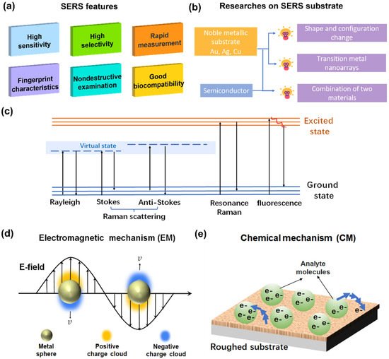
Figure 1. (a) Features of SERS; (b) development of research on SERS substrate; (c) schematic of Raman scattering; (d) EM: surface plasmon resonance on metal surface; (e) CM: charge transfer between analyte molecules and roughed substrate.
Electromagnetic mechanism (EM) is considered the leading cause of the SERS phenomenon, represented by the surface plasmon resonance (SPR) model of the metal (Figure 1d), which has a long-range effect and has little to do with the type of adsorbent molecules [2][3][4][5]. Surface plasmons were first observed in the spectrum of light diffracted on a metallic diffraction grating. It was soon proven that the anomaly was associated with the excitation of electromagnetic surface waves on the surface of the diffraction grating [6]. It was recognized that under the action of the photoelectric field, electrons near the metal surface would produce dense vibrations, causing excitation of the plasmons, especially on a rough surface [7]. Once the incident light frequency matches the oscillation frequency of electrons near the metal surface, a local surface plasma resonance occurs. Then, the electromagnetic field in the vicinity of the nanoparticles is significantly enhanced [8]. The electromagnetic enhancement also includes the image field enhancement [9] and tip lightning rod effect [10], though their contribution is smaller than the SPR mentioned above.
Chemical mechanism (CM) refers to the charge resonance transition generated by the interaction between molecule and substrate (Figure 1e), as well as charge transfer between analyte molecules. Unlike EM, CM has a short-range effect and mainly depends on the type of adsorbent molecules and the interplay between detected molecules and the substrate [11][12]. Because of the complexity of the substrate and the detection of molecular species, CM is far more complicated than EM [13].
CM primarily suggests that electrons in the metal are excited to the charge-transfer state under laser irradiation of appropriate wavelength, which causes relaxation of the molecular nuclear skeleton. Therefore, when the electron returns to the metal, the photon emitted is one less vibrational quantum of energy than the incoming light. The enhancement is caused by the resonance of the scattering process with the charge-transfer state [14].
2. MoS2-Related SERS Mechanism
It was proven that the EF of 2D monolayer MoS2 as SERS substrate to detect 4-Mercaptopyridine could reach 105, much higher than the previous observation on 2D graphene and boron nitride [15]. This considerable enhancement in the SERS signal is probably attributed to interface dipole interaction and the enhanced charge transfer from 2D MoS2 to organic molecules when in resonance [16]. Although the enhancement mechanism of the metal/MoS2 composite substrate is not well understood, theorists generally believe that both EM and CM make contributions.
One of the more plausible explanations is that since the Fermi level of MoS2 is higher than that of Au nanoparticles, Au nanoparticles act as the electron capture centers in the conduction band of MoS2, resulting in the transfer of electrons from MoS2 to Au. Therefore, potential changes and the formation of the Schottky barrier occur on the surface of MoS2 . This process, together with the electromagnetic enhancement of Au nanoparticles, remarkably enhances the Raman signal [17]..
Another explanation takes the more general interaction between semiconductors and metals into account and suggests that light exposure plays a crucial role in enhancing the Raman signal. In this course, two conditions may contribute to signal enhancement. First, owing to the localized surface plasmon resonance (LSPR) of metal nanocrystals, local enhanced electromagnetic fields are generated on the surface. When the metal nanocrystals are close enough to MoS2, the local electromagnetic field and the absorption spectrum of MoS2 overlap, which promotes the electron transfer from the valence band to the MoS2 conduction band and generates electron-hole pairs. Because of the strong field of the metal nanocrystals, the intensity of this process is increased by several orders of magnitude relative to light alone. During their interaction, the enhancement effect of the Raman signal is further amplified. The other functioning mechanism is related to plasmonic sensitization. In simple terms, the laser-induced plasmonic sensitization excites electrons in the conduction band of metal nanocrystals to overcome the Schottky barrier and jump into the conduction band of MoS2. The electromagnetic and chemical enhancements are amplified by plasma excitation and electron transfer during the entire process.
3. Hybrid SERS Nanostructures Based on MoS2
3.1. Synthesis of MoS2-Related SERS Substrates
Different research groups have prepared MoS2-based SERS substrate using diverse methods. They have found differences in the final enhancement effect through comparison, which implies that preparation technology can influence the efficiency and detection sensitivity of Surface-enhanced Raman scattering (SERS) to some extent [19][20][21][22][23][24]. The preparation methods of SERS substrates have been constantly updated and developed with the development of preparation technology. In the following, it was described some classical preparation methods and discuss the effect of impurities and defects introduced during the preparation process on the detection limits.
3.1.1. Synthesis of MoS2
Currently, there is a wide variety of preparation technologies for SERS substrates to MoS2. The following are some traditional approaches, namely the hydrothermal/solvothermal method, chemical vapor deposition (CVD) method and mechanical force stripping method.
Hydrothermal/Solvothermal Method
The hydrothermal/solvothermal method uses molybdenum-containing compounds as molybdenum sources and high-purity sulfur compounds as sulfur sources and surfactants. These two are mixed by reaction, and the liquid sample mixture is acquired after complete stirring. The mixture is then dried, heated and molded through a closed-kettle under high temperature. In the sealed heating process, MoS2 substrates with different morphologies can be obtained by controlling the reaction time, temperature and the number of reaction reagents. For instance, Jiang et al. [25] used Na2MoO4·2H2O (molybdenum sources), CH3CSNH2 (sulfur sources) and H4[Si(W3O10)4]·xH2O to collect deposited MoS2 in the autoclave. It was employed as SERS substrate to detect carbohydrate antigen 19-9 in serum directly, and the final minimum detection concentration reached 10−14 mol·L−1 level.
Chemical Vapor Deposition (CVD)
The CVD method is one of the traditional methods for the preparation of large-area nanofilm materials [26]. After decades of technical innovation, it is considered a mature technology for preparing 2D nanofilm materials [27][28]. The preparation process involves placing the growth base in a CVD tubular furnace, passing it through the precursor gas and allowing it to react on the surface of the substrate [29]. In preparing MoS2 nanosheet films by the CVD method, Mo is first sputtered on SiO2 substrate, then MoS2 nanometer-thin films are grown on the surface through the reaction between Mo and sulfur vapor in the furnace. The size and thickness of the MoS2 substrate can be modulated artificially by altering the thickness of Mo metal films. Zhan and colleagues [30] used this method to deposit Mo on the SiO2 substrate surface and fabricated a MoS2 thin-film layer by heating sulfur powder and reacting with Mo at a high temperature. Zheng et al. [31] used electrochemically oxidized Mo foil as a growth material to achieve layer-by-layer growth of MoS2 by rapid sulfidation of Mo oxides in the gas phase.
Mechanical Stripping Method
The mechanical stripping method applies the viscosity of special tape to act on the surface of MoS2 material to weaken Van der Waals forces of MoS2 between layers. Without breaking the covalent bond, MoS2 layered structure or even a single layer structure can be obtained. The thin layer is attached to the SiO2/Si substrate surface to form a MoS2 substrate. Yan et al. [32] obtained MoS2 substrate for Rh6G molecule detection with a minimum detection limit of 10−8 mol·L−1 by the mechanical stripping method combined with heating and annealing treatments.
3.1.2. Synthesis of Metal/MoS2 Hybrid Substrate
Recent approaches to prepare metal/MoS2 hybrids substrates for SERS can be organized into three categories: (1) physical methods: physically depositing specific metal on MoS2 or placing ready-made metal nanoparticles on MoS2 directly; (2) chemical methods: spontaneous reduction method, self-assembly technology, thermal reduction method (including hydrothermal method, solvothermal method, microwave-assisted hydrothermal method), among others; (3) nanoetching methods: plasma etching, electron beam lithography (EBL) and photoetching. It was emphatically described the latter two approaches.
Spontaneous Reduction Method
The spontaneous reduction method refers to the initiative reduction reaction between the prepared MoS2 film and the precursor solution of metal nanoparticles such as HAuCl4 solution (the precursor of gold NPs), to obtain directly the metal/MoS2 composite substrate. This spontaneous reduction can occur at room temperature or more uniformly and rapidly through auxiliary means such as heating [20][33].
Hydrothermal Reduction Method
Hydrothermal reduction is the process of reducing metal cations in solution under different conditions while adding MoS2 material. The cations are attracted by unsaturated sulfur on the MoS2 surface to form chemical bonds, and eventually the metal/MoS2 composite SERS substrate is obtained. Singha’s group [34] adopted the hydrothermal method to modify MoS2 with Au NPs and detected free bilirubin in human blood, which showed high sensitivity, stability and good reproducibility. However, compared with the traditional hydrothermal method, the microwave-assisted hydrothermal method is more frequently used to prepare nanomaterials [20][35][36]. Microwaves are utilized as a heating tool to realize stirring on the molecular level. It overcomes the shortcoming of uneven heating in the hydrothermal vessel, thus shortening reaction time and improving efficiency [37][38][39]. Kim and coworkers [40] reported this facile method and observed that the gold nanoparticles tend to grow at defective sites, mainly at the edges and the line defects in the basal planes.
Nanoetching Method
Nanoetching technology was first applied in the integrated process and had irreplaceable advantages in micrographics [41]. Its advantages such as fast processing speed, high precision, minor damage to substrates and no pollution make it a popular technique.
The typical representative of electron beam processing is electron beam lithography (EBL), which mainly uses electron beams to induce surface reaction beams for microprocessing. The reaction between the atoms on the substrate surface and the adsorbed molecules or ions is facilitated by irradiating the specimen by the electron beam, and the designed pattern is finally obtained on the substrate by the liftoff technique. Zhai et al. [42] applied EBL to fabricate a Au nanoarray on the monolayer MoS2 film, which was used as a SERS substrate to realize CV detection of 10−6–10−15 M. They considered it to be combined with the separation technology to form a sensor that can quickly detect trace molecules in a natural environment.
The focused laser beam can locally transform the MoS2 film into microscopic patterns with active nucleation sites. When the modified film is in complete contact with the reaction substance, selective modification can be achieved at specific locations to flexibly prepare a thin layer of MoS2 decorated by metal NPs. Lu and coworkers [43] employed this technology to realize self-designed pattern preparation of Au NPs decorating MoS2. They controlled the localized modification of the materials by changing the laser power, MoS2 film thickness and reaction time. It was proven that the prepared hybrid substrate can detect aromatic organic molecules with outstanding performance.
The femtosecond laser is another technique that is widely adopted to modify MoS2 with metal NPs [21][23]. It can induce photoelectrons generated on the film surface and greatly promote the interaction between metal cations and photoelectrons on the film surface. Then, the reduction and in situ deposition of metal NPs on MoS2 nanosheets formed the metal/MoS2 hybrid substrates for SERS.
Nanoetching technology possesses unique advantages in terms of precise tuning. The roughness of the laser-treated MoS2 film is about three times greater than that of the pristine, which facilitates the deposition of metal nanoparticles [43]. The hybrid substrates prepared by this method show stronger SERS activity, whose detection limit can reach as low as 1 fM for CV detection. In addition, the power of the laser also affects the Raman intensity at the same concentration of the analytes [42].
3.2. Advances in MoS2-Based SERS Substrate
3.2.1. MoS2 Substrates
With the development of chemical mechanisms, SERS substrate material is not confined to metal, and MoS2 emerges as a promising substrate material owing to its distinct merits shown in SERS studies. For single MoS2 material research, researchers have placed more focus on 2D material, which can be roughly divided into two directions: (1) special treatment of MoS2 material, such as plasma treatment and usage of the femtosecond laser to induce defect sites on the surface to enhance the charge transfer; and (2) stacking the single-layer 2D MoS2 material according to the set angle to obtain double-layer MoS2.
For the former research direction, it was found that the plasma-processed MoS2 nanosheets can perform better in SERS. The Raman intensities of Rh6G on MoS2 nanoflakes were enhanced more than tenfold after oxygen-plasma and argon-plasma treatments [44]. Other external treatments such as pressure and femtosecond laser were verified that they could reinforce charge transfer between the substrate and molecules to induce MoS2 defect sites and realize pressure or photoluminescence control [45][46][47]. Sun et al. [47] found that there are more transferred charges between the substrate and analytes with increasing applied pressure, which also leads to an increase in the enhancement factor. For the latter, Xia and coworkers [48] studied prominent resonance Raman and photoluminescence spectroscopic differences between AB and AA stacked bilayer MoS2, and considered that the 0° stacked MoS2 bilayer was superior to the 60° stacked one in interlayer electron coupling, hence its Raman enhancement effect was more outstanding.
Compared with metal, MoS2 possesses unique adsorption capacity, especially for some aromatic molecules, because the π bonds of MoS2 interplay with those of aromatic molecules [43][49]. Furthermore, MoS2 has good fluorescence quenching ability and can quench background fluorescence, which is conducive to detection and substrate stability at low concentration [50][51]. However, its electromagnetic enhancement is extremely weak, and chemical enhancement alone can hardly contribute significantly to sensitivity. In addition, owing to the selectivity and complexity of chemical enhancement for the detection of molecules, these substrates can only be implemented for some particular organic molecules such as aromatic molecules.
3.2.2. Metal/MoS2 Hybrid Substrates
Metal/MoS2 hybrid substrates are considered admirable SERS substrates, with EFs that can reach 108 and even up to 1012 after some special processing such as changing shape and metal nanoparticles configuration [52]. Because of the prominent enhancement effect of this substrate, experimentalists have conducted various studies on it, making this kind of substrate become one of the important research topics of SERS in recent years.
One was on Au NPs /MoS2, and the researchers found that these composite substrates enhanced significantly better than either single Au or single MoS2. Subsequently, Rani et al. [53] used low-power focused laser cutting to carve artificial edges on the MoS2 monolayer. The intensive accumulation of Au NPs along the artificial edges led to the aggregation of SERS hotspots in the same places, which made it possible to generate SERS hotspots with ideal location and geometry shape in a controllable way on a large-area substrate. Liang’s group [54] prepared 3D MoS2-nanospheres, 3D MoS2-nanospheres @Au seeds and 3D MoS2-nanospheres @Ag-NPs hybrids structures, and calculated their enhancement factors as 500, 7.5 × 10⁶ and 1.2 × 10⁸, respectively. Through experiments, they believed that silver nanoparticles were more suitable than gold nanoparticles as modification materials for MoS2. This is because silver nanoparticles can be closer to each other and have higher coverage, leading to more hotspots on the surface and stronger signal enhancement.
Compared with the substrates mentioned above, the metal/MoS2 hybrid substrate concentrated the advantages of metal and MoS2, so it shows better adsorption effect, higher sensitivity, stronger stability and lower detection limit, and has gradually become a new platform in SERS research. Because of the modification of MoS2 by metal nanoparticles, the composite substrate exhibits not only stronger electromagnetic enhancement, but also better chemical enhancement effect and fluorescence quenching effect, which can greatly reduce external interference. However, owing to the unclear mechanisms of the interaction between metal and MoS2 and the complicated production process, further development of this kind of substrate has been limited to some extent.
References
- Yu, Z.; Brus, L. Rayleigh and Raman scattering from individual carbon nanotube bundles. J. Phys. Chem. B 2001, 105, 1123–1134.
- Otto, A. Theory of first layer and single molecule Surface Enhanced Raman Scattering (SERS). Phys. Status Solidi (a) 2001, 188, 1455–1470.
- Tian, X.; Chen, L.; Xu, H.; Sun, M. Ascertaining genuine SERS spectra of p-aminothiophenol. RSC Adv. 2012, 2, 8289–8292.
- Willets, K.A.; Van Duyne, R.P. Localized surface plasmon resonance spectroscopy and sensing. Annu. Rev. Phys. Chem. 2007, 58, 267–297.
- Meyer, S.A.; Le Ru, E.C.; Etchegoin, P.G. Combining Surface Plasmon Resonance (SPR) Spectroscopy with Surface-Enhanced Raman Scattering (SERS). Anal. Chem. 2011, 83, 2337–2344.
- Homola, J. Electromagnetic Theory of Surface Plasmons. In Surface Plasmon Resonance Based Sensors; Homola, J., Ed.; Springer: Berlin/Heidelberg, Germany, 2006; Volume 4, pp. 3–44.
- Zhao, J.; Zhang, C.; Lu, Y.; Wu, Q.; Yuan, Y.; Xu, M.; Yao, J. Surface-enhanced Raman spectroscopic investigation on surface plasmon resonance and electrochemical catalysis on surface coupling reaction of pyridine at Au/TiO2 junction electrodes. J. Raman Spectrosc. 2020, 51, 2199–2207.
- Schwartzberg, A.M.; Zhang, J.Z. Novel optical properties and emerging applications of metal nanostructures. J. Phys. Chem. C 2008, 112, 10323–10337.
- David, C.; Richter, M.; Knorr, A.; Weidinger, I.; Hildebrandt, P. Image dipoles approach to the local field enhancement in nanostructured Ag–Au hybrid devices. J. Chem. Phys. 2010, 132, 24712.
- Liao, P.F.; Wokaun, A. Lightning rod effect in surface enhanced Raman scattering. J. Chem. Phys. 1982, 76, 751–752.
- Schlücker, S. Surface-Enhanced Raman Spectroscopy: Concepts and chemical applications. Angew. Chem. Int. Ed. 2014, 53, 4756–4795.
- Kovacs, G.J.; Loutfy, R.O.; Vincett, P.S.; Jennings, C.; Aroca, R. Distance dependence of SERS enhancement factor from Langmuir-Blodgett monolayers on metal island films: Evidence for the electromagnetic mechanism. Langmuir 1986, 2, 689–694.
- Ma, N.; Zhang, X.-Y.; Fan, W.; Han, B.; Jin, S.; Park, Y.; Chen, L.; Zhang, Y.; Liu, Y.; Yang, J.; et al. Controllable preparation of SERS-active Ag-FeS Substrates by a cosputtering technique. Molecules 2019, 24, 551.
- Moore, J.E.; Morton, S.M.; Jensen, L. Importance of correctly describing charge-transfer excitations for understanding the chemical effect in SERS. J. Phys. Chem. Lett. 2012, 3, 2470–2475.
- Muehlethaler, C.; Considine, C.R.; Menon, V.; Lin, W.-C.; Lee, Y.-H.; Lombardi, J.R. Ultrahigh Raman enhancement on monolayer MoS2. ACS Photon. 2016, 3, 1164–1169.
- Xia, M. 2D materials-coated plasmonic structures for sers applications. Coatings 2018, 8, 137.
- Shakya, J.; Patel, A.S.; Singh, F.; Mohanty, T. Composition dependent Fermi level shifting of Au decorated MoS2 nanosheets. Appl. Phys. Lett. 2016, 108, 013103.
- Bhanu, U.; Islam, M.R.; Tetard, L.; Khondaker, S.I. Photoluminescence quenching in gold—MoS2 hybrid nanoflakes. Sci. Rep. 2015, 4, 5575.
- Sha, P.; Su, Q.; Dong, P.; Wang, T.; Zhu, C.; Gao, W.; Wu, X. Fabrication of () nanorods as a SERS substrate by the oblique angle deposition process and sputtering technology. RSC Adv. 2021, 11, 27107–27114.
- Su, S.; Zhang, C.; Yuwen, L.; Chao, J.; Zuo, X.; Liu, X.; Song, C.; Fan, C.; Wang, L. Creating SERS hot spots on MoS2 nanosheets with in situ grown gold nanoparticles. ACS Appl. Mater. Interfaces 2014, 6, 18735–18741.
- Pan, C.; Song, J.; Sun, J.; Wang, Q.; Wang, F.; Tao, W.; Jiang, L. One-step fabrication method of MoS2 for high-performance surface-enhanced Raman scattering. J. Phys. Chem. C 2021, 125, 24550–24556.
- Miao, P.; Ma, Y.; Sun, M.; Li, J.; Xu, P. Tuning the SERS activity and plasmon-driven reduction of p-nitrothiophenol on a 2 film. Faraday Discuss. 2019, 214, 297–307.
- Zuo, P.; Jiang, L.; Li, X.; Li, B.; Ran, P.; Li, X.; Qu, L.; Lu, Y.F. Metal (Ag, Pt)–MoS2 hybrids greenly prepared through photochemical reduction of femtosecond laser pulses for SERS and HER. ACS Sustain. Chem. Eng. 2018, 6, 7704–7714.
- Er, E.; Hou, H.-L.; Criado, A.; Langer, J.; Möller, M.; Erk, N.; Liz-Marzán, L.M.; Prato, M. High-yield preparation of exfoliated 1T-MoS2 with SERS activity. Chem. Mater. 2019, 31, 5725–5734.
- Jiang, J.; Shen, Q.; Xue, P.; Qi, H.; Wu, Y.; Teng, Y.; Zhang, Y.; Liu, Y.; Zhao, X.; Liu, X. A highly sensitive and stable SERS sensor for malachite green detection based on Ag nanoparticles in situ generated on 3D MoS2 nanoflowers. ChemistrySelect 2020, 5, 354–359.
- Lee, Y.-H.; Zhang, X.-Q.; Zhang, W.; Chang, M.-T.; Lin, C.-T.; Chang, K.-D.; Yu, Y.-C.; Wang, J.T.-W.; Chang, C.-S.; Li, L.-J.; et al. Synthesis of large-area MoS2 atomic layers with chemical vapor deposition. Adv. Mater. 2012, 24, 2320–2325.
- Liu, H.F.; Wong, S.L.; Chi, D.Z. CVD growth of MoS2-based two-dimensional materials. Chem. Vap. Depos. 2015, 21, 241–259.
- Jeon, J.; Jang, S.K.; Jeon, S.M.; Yoo, G.; Jang, Y.H.; Park, J.-H.; Lee, S. Layer-controlled CVD growth of large-area two-dimensional MoS2 films. Nanoscale 2015, 7, 1688–1695.
- Kumar, M.; Ando, Y. Chemical vapor deposition of carbon nanotubes: A review on growth mechanism and mass production. J. Nanosci. Nanotechnol. 2010, 10, 3739–3758.
- Zhan, Y.; Liu, Z.; Najmaei, S.; Ajayan, P.M.; Lou, J. Large-area vapor-phase growth and characterization of MoS2 atomic layers on a SiO2 Substrate. Small 2012, 8, 966–971.
- Zheng, J.; Yan, X.; Lu, Z.; Qiu, H.; Xu, G.; Zhou, X.; Wang, P.; Pan, X.; Liu, K.; Jiao, L. High-mobility multilayered MoS2 flakes with low contact resistance grown by chemical vapor deposition. Adv. Mater. 2017, 29, 1604540.
- Yan, D.; Qiu, W.; Chen, X.; Liu, L.; Lai, Y.; Meng, Z.; Song, J.; Liu, Y.; Liu, X.-Y.; Zhan, D. Achieving high-performance surface-enhanced Raman scattering through one-step thermal treatment of bulk MoS2. J. Phys. Chem. C 2018, 122, 14467–14473.
- Fei, X.; Liu, Z.; Hou, Y.; Li, Y.; Yang, G.; Su, C.; Wang, Z.; Zhong, H.; Zhuang, Z.; Guo, Z. Synthesis of Au 2 quantum dots nanocomposites for SERS bio-analysis and label-free bio-imaging. Materials 2017, 10, 650.
- Singha, S.S.; Mondal, S.; Bhattacharya, T.S.; Das, L.; Sen, K.; Satpati, B.; Das, K.; Singha, A. Au nanoparticles functionalized 3D-MoS2 nanoflower: An efficient SERS matrix for biomolecule sensing. Biosens. Bioelectron. 2018, 119, 10–17.
- Liang, X.; Zhang, X.-J.; You, T.-T.; Yang, N.; Wang, G.-S.; Yin, P.-G. Three-dimensional MoS2 hybrids as SERS sensor for quantitative and ultrasensitive detection of melamine in milk. J. Raman Spectrosc. 2018, 49, 245–255.
- Vattikuti, S.P.; Nagajyothi, P.; Devarayapalli, K.; Yoo, K.; Nam, N.D.; Shim, J. Hybrid Ag/MoS2 nanosheets for efficient electrocatalytic oxygen reduction. Appl. Surf. Sci. 2020, 526, 146751.
- Yu, H.-P.; Zhu, Y.-J.; Lu, B.-Q. Highly efficient and environmentally friendly microwave-assisted hydrothermal rapid synthesis of ultralong hydroxyapatite nanowires. Ceram. Int. 2018, 44, 12352–12356.
- Kharisov, B.I.; Kharissova, O.V.; Ortiz-Mendez, U. (Eds.) Microwaves: Microwave-Assisted Hydrothermal Synthesis of Nanoparticles. In CRC Concise Encyclopedia of Nanotechnology; CRC Press: Boca Raton, FL, USA, 2016; pp. 588–599.
- Yu, X.; Zhao, Z.; Sun, D.; Ren, N.; Yu, J.; Yang, R.; Liu, H. Microwave-assisted hydrothermal synthesis of Sn3O4 nanosheet/rGO planar heterostructure for efficient photocatalytic hydrogen generation. Appl. Catal. B Environ. 2018, 227, 470–476.
- Kim, J.; Byun, S.; Smith, A.J.; Yu, J.; Huang, J. Enhanced electrocatalytic properties of transition-metal dichalcogenides sheets by spontaneous gold nanoparticle decoration. J. Phys. Chem. Lett. 2013, 4, 1227–1232.
- Kang, S. Replication technology for micro/nano optical components. Jpn. J. Appl. Phys. 2004, 43, 5706–5716.
- Zhai, Y.; Yang, H.; Zhang, S.; Li, J.; Shi, K.; Jin, F. Controllable preparation of Au-MoS2 nano-array composite: Optical properties study and SERS application. J. Mater. Chem. C 2021, 9, 6823–6833.
- Lu, J.; Lu, J.H.; Liu, H.; Liu, B.; Gong, L.; Tok, E.S.; Loh, K.P.; Sow, C.H. Microlandscaping of Au Nanoparticles on few-layer MoS2 films for chemical sensing. Small 2015, 11, 1792–1800.
- Sun, L.; Hu, H.; Zhan, D.; Yan, J.; Liu, L.; Teguh, J.S.; Yeow, E.K.L.; Lee, P.S.; Shen, Z. Plasma modified MoS2 nanoflakes for surface enhanced Raman scattering. Small 2014, 10, 1090–1095.
- Zuo, P.; Jiang, L.; Li, X.; Ran, P.; Li, B.; Song, A.; Tian, M.; Ma, T.; Guo, B.; Qu, L.; et al. Enhancing charge transfer with foreign molecules through femtosecond laser induced MoS2 defect sites for photoluminescence control and SERS enhancement. Nanoscale 2019, 11, 485–494.
- Sun, H.; Yao, M.; Liu, S.; Song, Y.; Shen, F.; Dong, J.; Yao, Z.; Zhao, B.; Liu, B. SERS selective enhancement on monolayer MoS2 enabled by a pressure-induced shift from resonance to charge transfer. ACS Appl. Mater. Interfaces 2021, 13, 26551–26560.
- Sun, H.; Yao, M.; Song, Y.; Zhu, L.; Dong, J.; Liu, R.; Li, P.; Zhao, B.; Liu, B. Pressure-induced SERS enhancement in a MoS2/Au/R6G system by a two-step charge transfer process. Nanoscale 2019, 11, 21493–21501.
- Xia, M.; Li, B.; Yin, K.; Capellini, G.; Niu, G.; Gong, Y.; Zhou, W.; Ajayan, P.M.; Xie, Y.-H. Spectroscopic signatures of AA′ and AB stacking of chemical vapor deposited bilayer MoS2. ACS Nano 2015, 9, 12246–12254.
- Lai, H.; Ma, G.; Shang, W.; Chen, D.; Yun, Y.; Peng, X.; Xu, F. Multifunctional magnetic sphere-MoS2@Au hybrid for surface-enhanced Raman scattering detection and visible light photo-Fenton degradation of aromatic dyes. Chemosphere 2019, 223, 465–473.
- Tegegne, W.A.; Su, W.-N.; Tsai, M.-C.; Beyene, A.B.; Hwang, B.-J. Ag nanocubes decorated 1T-MoS2 nanosheets SERS substrate for reliable and ultrasensitive detection of pesticides. Appl. Mater. Today 2020, 21, 100871.
- Li, Z.; Jiang, S.; Xu, S.; Zhang, C.; Qiu, H.; Li, C.; Sheng, Y.; Huo, Y.; Yang, C.; Man, B. Few-layer MoS2-encapsulated Cu nanoparticle hybrids fabricated by two-step annealing process for surface enhanced Raman scattering. Sens. Actuators B Chem. 2016, 230, 645–652.
- Zeng, Z.; Tang, D.; Liu, L.; Wang, Y.; Zhou, Q.; Su, S.; Hu, D.; Han, B.; Jin, M.; Ao, X.; et al. Highly reproducible surface-enhanced Raman scattering substrate for detection of phenolic pollutants. Nanotechnology 2016, 27, 455301.
- Rani, R.; Yoshimura, A.; Das, S.; Sahoo, M.R.; Kundu, A.; Sahu, K.K.; Meunier, V.; Nayak, S.K.; Koratkar, N.; Hazra, K.S. Sculpting artificial edges in monolayer MoS2 for controlled formation of surface-enhanced Raman hotspots. ACS Nano 2020, 14, 6258–6268.
- Liang, X.; Wang, Y.-S.; You, T.-T.; Zhang, X.-J.; Yang, N.; Wang, G.-S.; Yin, P.-G. Interfacial synthesis of a three-dimensional hierarchical MoS2 nanocomposite as a SERS nanosensor for ultrasensitive thiram detection. Nanoscale 2017, 9, 8879–8888.
More
Information
Subjects:
Spectroscopy
Contributor
MDPI registered users' name will be linked to their SciProfiles pages. To register with us, please refer to https://encyclopedia.pub/register
:
View Times:
1.8K
Revisions:
2 times
(View History)
Update Date:
25 Mar 2022
Table of Contents


Notice
You are not a member of the advisory board for this topic. If you want to update advisory board member profile, please contact office@encyclopedia.pub.
OK
Confirm
Only members of the Encyclopedia advisory board for this topic are allowed to note entries. Would you like to become an advisory board member of the Encyclopedia?
Yes
No
${ textCharacter }/${ maxCharacter }
Submit
Cancel
Back
Comments
${ item }
|
${ item.createdUser.fullName }
${ item.createdAt }
${ item.vote }
${ item.reply }
Delete
${ reply.createdUser.fullName }
${ reply.createdAt }
${ reply.vote }
Delete
There is no reply to this comment~
${ item.replyTextCharacter }/${ item.replyMaxCharacter }
Submit
Cancel
More
No more~
There is no comment~
${ textCharacter }/${ maxCharacter }
Submit
Cancel
${ selectedItem.replyTextCharacter }/${ selectedItem.replyMaxCharacter }
Submit
Cancel
Confirm
Are you sure to Delete?
Yes
No