 +1 credit
| Version | Summary | Created by | Modification | Content Size | Created at | Operation |
|---|---|---|---|---|---|---|
| 1 | Catherine Langpoklakpam | + 2864 word(s) | 2864 | 2022-02-25 02:35:11 | | | |
| 2 | Jessie Wu | Meta information modification | 2864 | 2022-03-21 02:01:10 | | | | |
| 3 | Jessie Wu | Meta information modification | 2864 | 2022-03-21 02:20:59 | | | | |
| 4 | Jessie Wu | -5 word(s) | 2859 | 2022-03-21 02:22:38 | | |
Video Upload Options
Owing to the superior properties of silicon carbide (SiC), such as higher breakdown voltage, higher thermal conductivity, higher operating frequency, higher operating temperature, and higher saturation drift velocity, SiC has attracted much attention from researchers and the industry for decades. With the advances in material science and processing technology, many power applications such as new smart energy vehicles, power converters, inverters, and power supplies are being realized using SiC power devices. In particular, SiC MOSFETs are generally chosen to be used as a power device due to their ability to achieve lower on-resistance, reduced switching losses, and high switching speeds than the silicon counterpart and have been commercialized extensively in recent years.
1. Introduction
The development of power electronics technology has always been towards achieving higher power density, higher efficiency, and integrating many systems where power semiconductor devices (power devices) play an important role in this development. Over the last 50 years, the advancements of power devices have been primarily due to Si-based power devices. However, due to limitations of the intrinsic physical properties of Si, devices based on Si cannot be used for future power devices. The introduction of wide-bandgap (WBG) semiconductor materials such as silicon carbide (SiC) and gallium nitride (GaN) materials have been a revolutionary development in the field of power devices. The superior material properties of WBG materials, such as higher dielectric strength, higher saturation drift velocity, and the ability to operate in harsh environments, make the materials favorable for power devices. GaN-based devices are mainly used for high-frequency applications, while SiC-based devices are used for high voltage power applications. The larger critical electric field, higher thermal conductivity, and higher breakdown voltage enable SiC-based devices to operate at higher current density, higher temperature, and higher blocking voltage. Hence, for more than a decade, SiC-based power components have been a topic for extensive research for high voltage/power applications. Moreover, SiC is more mature in terms of the quality of the crystal [1], the existence of large wafers [2], and is readily available in the market[3]. In addition, the material cost of SiC is much lesser than that of GaN [4], and the processing lines of SiC-based devices have great compatibility with that of Si-based devices.
2. SiC Applications
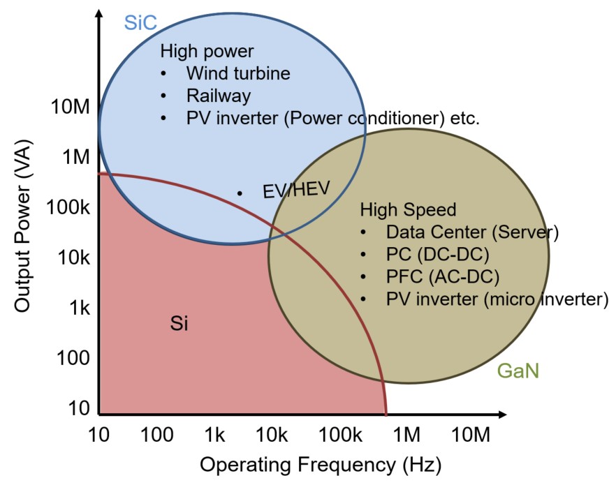
The high-performance capabilities of SiC power devices provide a significant improvement in the existing systems, enabling new power applications. In addition, the outstanding material and chemical properties of SiC, namely, high thermal conductivity, high breakdown electric field, low intrinsic carrier concentration, and high chemical inertness, make SiC-based devices favorable devices for implementing in high-temperature electronics as well as in thermal sensors that can also be used in harsh environments [5]. Moreover, the lower on-resistance and the lower output capacitance of SiC MOSFET makes it an appropriate choice to be used in switching designs such as three-phase inverters, digital power supplies, and also for electronic AC-to-DC or DC-to-DC converters. In addition, the reduced switching losses of SiC devices also improve the switching frequencies of the converters. Hence, SiC power devices play an important role in high-performance power device applications. At present, SiC-based converters are used in solar inverters[6][7], EV/HEV drivers (e.g., SiC MOSFETs at Tesla Model 3 EVs) [8][9], railway traction inverters [10], high voltage applications[11], and uninterrupted power supplies (UPSs). The cost of a solar inverter was reduced by 20% of the power by using SiC diodes and SiC JFETs [12]. Figure 1 illustrates the classification of various types of applications based on Si and WBG devices[13]. As seen in the figure, Si devices are used for lower power and lower frequency applications, while GaN-based devices are used for lower voltage and lower power high-frequency applications such as data centers and consumer systems; SiC devices are used for higher power, higher voltage switching power applications such as trains, electric vehicles and their battery chargers, and industrial automation.
3. SiC MOSFETs
Since the beginning, MOSFETs have been the most successful devices and are mainly employed for switching operations in power converters [18]. The structure of SiC power MOSFETs is similar to that of Si MOSFETs with an insulated gate structure. SiC power MOSFETs can operate over a wide range of blocking voltage, with lower conduction and switching loss, as the device has less on-resistance than the Si counterpart and is much smaller[19]. The main advantage of SiC power MOSFETs is that the SiC power MOSFET combines the excellent material properties of SiC, which enhances the performance of the device. However, the SiC power MOSFET suffers from the carbon cluster introduction at the gate oxygen interface, which increases Dit at the gate–oxide interface, and thus, the channel resistance increases.
SiC Power MOSFETs are classified into different types depending on the structural modification of the gate and the drift region. The classification of the device is illustrated in Figure 2. The two basic types of SiC MOSFET structures based on the gate modification are planar MOSFETs (DMOSFETs) and trench MOSFETs (UMOSFETs) [20], as shown in figure 2(a) and (b), respectively. The planar types are further classified into conventional and super junction MOSFETs (SJ MOSFETs), as shown in Figure2 (a) the conventional and Figure 2(c) super junction MOSFET. A detailed discussion on the types of SiC MOSFETs can be found in the following sections.
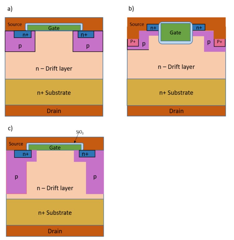
Figure 2. Different types of MOSFET structures a) Planar MOSFET b) Trench MOSFET and c) Superjunction MOSFET.
3.1. Planar and Trench MOSFETs
The planar MOSFETs (or DMOSFETs), as shown in Figure 2(a), are a double diffusion MOS structure where the channel is formed by a double diffusion process and has the ability to withstand high voltage. However, the performance of the device is affected by the poor channel mobility due to the scattering process at the interface of the 4H-SiC/insulator. This scattering causes a significant reduction in mobility at the interface when compared with that of the bulk. Moreover, the presence of parasitic junction FET resistance increases the conduction loss during the forward condition[21]. A 4H-SiC Planar MOSFET with a blocking voltage of 2.3 kV was proposed in [22]. The device has an acceptable gate oxide electric field with a gate oxide thickness of 27 nm. The device was fabricated using a commercial foundry. The device exhibits an improvement in Ron, sp, and a high-frequency figure of merit (FOM) by 1.3 times when a 15 V is applied at the gate. However, the device suffers from gate voltage overshoot failure due to the thin gate oxide. A 4H-SiC Planar MOSFET with multiple floating guard-rings for edges termination was developed; the device can achieve a blocking voltage of 2.4 kV and a specific on-resistance of about 42 mΩ cm2 [23]. The fabricated device exhibits a mobility of 22 cm2/V.s in the channel and has a threshold voltage of about 8.5 V.
To minimize the conduction and switching loss in the planar MOSFET, the trench MOSFET or UMOSFET was developed for power application. The structure of trench MOSFET is shown in Figure 2 (b); it has a vertical gate channel in U groove shape and a channel form at the sidewalls of the trench. This structure improved the channel migration rate and was able to eliminate the parasitic JFET resistance. In addition, the on-resistance of the trench SiC MOSFET is half the planar SiC MOSFET. Hence, the trench SiC MOSFET design is preferred for power devices [24][25]. The first trench MOSFET was first introduced in 1992 by Palmour et al.[26]. However, the device suffers from low mobility in the inversion layer due to the presence of a high electric field at the trench corner in the oxide, which restricts the breakdown voltage of the device. A 1.2 kV trench gate SiC MOSFET with a low switching loss was developed by Fiji Electric [27]. The proposed device exhibits a 48% reduction in on-resistance, with a higher threshold voltage than the conventional SiC planar MOSFET. A 4H-SiC Planar MOSFET with a blocking voltage of 2.3 kV was proposed[22]. The device has an acceptable gate oxide electric field, with a gate oxide thickness of 27 nm. The device was fabricated using a commercial foundry. The device exhibits an improvement in the specific on-resistance and high-frequency figure of merit by 1.3 times when the applied gate bias is 15 V. However, the device suffers from gate voltage overshoot failure due to the thinner gate oxide. A 4H-SiC Planar MOSFET with multiple floating guard-rings for terminating the edges was developed; the device can achieve a blocking voltage of 2.4 kV and a specific on-resistance of about 42 mΩ cm2 [23]. The fabricated device exhibits a mobility of 22 cm2/V.s in the channel and has an 8.5 V threshold voltage. Purdue University introduced a trench MOSFET with a blocking voltage of 5 kV, with protection in the trench oxide and an extension in the junction termination[23][28].
The major issue of the common single trench is the concentration of the electric field at the bottom of the gate trench, which imposes a reliability issue to the device under long-term use. Additionally, it also suffers from the degradation of the switching performance and also the degradation of breakdown voltage due to the high value of gate-drain capacitance. To overcome the immature breakdown and reliability problem of the oxide, a double trench SiC MOSFET (DT MOS) was developed; it distributes the electric field concentration on the gate oxide into the source region[20][29][30]. The structure has a p+ shielding region to distribute the high gate oxide electric field to the source and drain p+ regions, which help in improving the breakdown voltage of the device [31]. The p+ shielding also improves the switching performance of the device by reducing the gate and drain charge coupling effect[32].
For high power switching applications, to increase the switching speed with lesser switching losses, a smaller value of reverse transfer capacitance (CGD) and lower gate-drain charge (QGD) is necessary. A split-gate double trench MOSFET (SG-MOSFET) was proposed, with a better high-frequency FOM (Ron, sp × QGD) than the DT MOS[33][34]. The structure has a separate upper and lower gate terminal; the upper gate terminal is connected to the gate voltage and is lower than the source voltage. The area under the active channel is reduced, which enhances the switching performance by reducing the gate-drain capacitance. Central implant MOSFET (CI MOSFET) is another type of structure demonstrated by Wolfspeed; it exhibits lower CGD and QGD [35]. In power inverter applications, to reduce the SiC Chip area, SiC MOSFETs are used with free-wheeling diodes (FWD), namely, parasitic body PiN diodes. However, these diodes result in bipolar degradation and increase on-state power dissipation[36]. To overcome these issues, a different variety of embedded parallel Schottky barrier diodes (SBDs) with SiC MOSFETs has been proposed[37][38][39][40][41][42][43].3.2. Superjunction MOSFETs
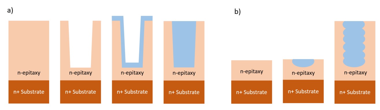
Superjunction (SJ) is a technique utilized widely to overcome the Ron, spxA limitation in Si devices [44]. A superjunction MOSFET (SJ MOSFET) structure shown in Figure 2 (c), has alternating p and n layers in the drift region. The structure is formed by penetrating p+ columns into the n-epitaxial layer and follows the charge compensation principle, which helps in distributing the electric field uniformly inside the drift region[45]. As a result, the performance of the SJ MOSFET surpasses the conventional MOSFET performance. The main benefit of SJ MOSFETs is the linear relationship between Ron, sp and the breakdown voltage (BV), whereas for conventional MOSFETs (planar), the relationship is Rsp, on ∝ BV2.4–2.6 [46]. Moreover, SJ can reduce the Ron, sp of the device without compromising the BV voltage of the device[44]. The structure of SJ MOSFETs can be grown by trench filling or by multi epitaxial growth. The epitaxial growth of SJ by trench filling is shown in Figure 3 (a) and by multi epitaxial growth in Figure 3 (b). The trench filling epitaxial growth process is done by dry etching at the beginning to form a deep trench, and then, on the trench surface, an epitaxial layer is grown in the trench [47][48]. The multi-epitaxial growth method is a fabrication method that is used to achieve a certain thickness of drift-layer by combining epitaxial growth and the ion implantation method of fabrication[49]. The fabrication process of the SJ structure was first introduced by R. Kosugi et al. [50]. The measured breakdown voltage and Ron, sp of the fabricated pn-pillar structure were 1545 V and 1.06 mΩ cm2, respectively; the structure has a 5.5-μm-thick pn-pillar structure, grown using multiple epitaxial growth method. The breakdown voltage and specific on-resistance achieved are almost the same as that of the theoretical limit of SiC. In addition, SiC-based SJ structures have been exhibited to show a reduction in on-resistance by 140 times and have a smaller pillar charge imbalance effect than the Si SJ structures [51].
SiC SJ MOSFETs have also exhibited an excellent Baliga’s figure of merit (FOM) (BV 2/Ron, sp) when compared with other SiC devices [52]. Simple analytical models for predicting the on-resistance and breakdown voltage of SiC SJ MOSFETs were proposed in [53][54]. Furthermore, SiC SJ MOSFETs exhibited a lower charge imbalance effect when compared with Si SJ MOSFETs in the drift region [51]. To achieve a better trade-off between the BV and Ron, sp, many researchers aimed to obtain the desired result by modifying the doping profile or the structure of the device. A SiC SJ MOSFET with a variation in the vertical doping profile (VVD) was proposed[45]; the device exhibits a better trade-off between the on-resistance and BV. The proposed device also shows the best results in both Baliga’s and conventional FOM. A SiC SJ V-groove trench MOSFET with a breakdown voltage of 820 V and an on-resistance of 0.97 mΩ cm2 was reported by Masuda et al. [55]. A SiC SJ V-groove trench MOSFET with a smaller on-resistance of 0.63 mΩ cm2 and a breakdown voltage of 1170 V was demonstrated in [56]. The proposed device has a lower on-resistance than the SiC MOSFETs with a breakdown voltage of over 600 V. A class of 1.2 kV SiC SJ MOSFETs, with an extremely low value of Ron, spxA, a higher value of withstanding the short-circuit capability, and a significantly lower value of reverse recovery loss, was demonstrated in [57][58][59]. A DC-FSJ MOSFET (different concentration floating super junction MOSFET) was proposed [60], and the device was able to achieve a breakdown voltage of more than 3.3 kV, along with reduced Ron, sp. The Ron, sp of the proposed structure was 25% less than conventional vertical MOSFET under the same conditions. The structure was fabricated by implementing multiple epitaxial growths with floating p-type structures and different concentrations of epitaxial layers. The BFOM of the device increased by 18% from FSJ MOSFETs and by 27% from vertical MOSFETs. A SiC SJ MOSFET with a very high breakdown voltage of 3.3 kV and a low Ron, sp of 3.3 mΩ cm2 at 27 °C and 6.2 mΩ cm2 at 175 °C was developed in [61]. The proposed devices were able to exceed the theoretical limit of the unipolar SiC device.
Although SiC power devices have come a long way in improving their performances and satisfying the increasing demands, it is noteworthy to mention one of the key technical challenges faced, i.e., the reduction of electric field on the surface or at the edges of the device. The reduction of the electric field becomes more challenging with device miniaturization. Some in-plane edge termination techniques have been demonstrated for SiC power devices, which have a similar concept to that of Si power devices. The techniques include field plates [62][63], mesa structures [64], junction termination expansion (JTE) [65][66][67], floating field rings (FFR)[68][69], ramp structures [70][71], ion implantation, and hybrid solutions[72][73][74][75][76]. Edge terminations are generally used at the device periphery so that it supports the maximum amount of the bulk breakdown value[77] . Hence, robust and reliable edge terminations are one of the most important requirements that help in achieving the full SiC technology potential.
4. Conclusion
SiC power devices are widely used in power applications and have been researched extensively in various industries and academics. Along with the inherited superior material properties of SiC, SiC-based devices are able to be used in high speed, high voltage, and high-temperature operations. Hence, SiC power devices are employed in power converters, high-efficiency power inverters, and also in smart electric vehicles. SiC power devices and its applications were discussed. In addition, the extensive discussion of the advancement of the most popular SiC devices (SiC MOSFETs) have also included. SiC power devices show great potential in achieving highly effective high-performance power applications.
References
- Tsunenobu Kimoto, James A. Cooper. Introduction. In Fundamentals of Silicon Carbide Technology: Growth, Characterization, Devices, and Applications; John Wiley & Sons: Hoboken, NJ, USA, 2014; pp. 1-10.
- Alton Horsfall; Saddow , Steven E, Anant Agarwal: Advances in silicon carbide processing and applications. BioMedical Engineering OnLine 2005, 4, 33-33, 10.1186/1475-925x-4-33.
- Vibhor Kumar; Sandeep Kumar; A. S. Maan; Jamil Akhtar; Interface improvement of epitaxial 4H-SiC based Schottky didoes by selective heavy ion irradiation. Applied Nanoscience 2020, -, 1-8, 10.1007/s13204-020-01608-3.
- Yuanhang Zhang; Comparison Between Competing Requirements of GaN and SiC Family of Power Switching Devices. IOP Conference Series: Materials Science and Engineering 2020, 738, 1-6, 10.1088/1757-899x/738/1/012004.
- Kumar, V.; Maan, A.S.; Akhtar, J. Barrier height inhomogeneities induced anomaly in thermal sensitivity of Ni/4H-SiC Schottky diode temperature sensor. J. Vac. Sci. Technol. B 2014, 32, 041203.
- M. H. Todorovic et al., "SiC MW PV Inverter," PCIM Europe 2016; International Exhibition and Conference for Power Electronics, Intelligent Motion, Renewable Energy and Energy Management, 2016, pp. 1-8.
- K. Fujii, Y. Noto, M. Oshima and Y. Okuma, "1-MW solar power inverter with boost converter using all SiC power module," 2015 17th European Conference on Power Electronics and Applications (EPE'15 ECCE-Europe), 2015, pp. 1-10, doi: 10.1109/EPE.2015.7309080.
- About the SiC MOSFETs modules in Tesla Model 3 . -. Retrieved 2022-3-17
- Ming Su; Chingchi Chen; Shrivatsal Sharma; Jun Kikuchi; Performance and cost considerations for SiC-based HEV traction inverter systems. 2015 IEEE 3rd Workshop on Wide Bandgap Power Devices and Applications (WiPDA) 2015, -, 347-350, 10.1109/wipda.2015.7369032.
- Katsumi Ishikawa; Seigo Yukutake; Yasuhiko Kono; Kazutoshi Ogawa; Norifumi Kameshiro; Traction inverter that applies compact 3.3 kV / 1200 A SiC hybrid module. 2014 International Power Electronics Conference (IPEC-Hiroshima 2014 - ECCE ASIA) 2014, -, 2140-2144, 10.1109/ipec.2014.6869884.
- Mrinal K. Das; Craig Capell; David E. Grider; Scott Leslie; John Ostop; Ravi Raju; Michael Schutten; Jeffrey Nasadoski; Allen Hefner; 10 kV, 120 A SiC half H-bridge power MOSFET modules suitable for high frequency, medium voltage applications. 2011 IEEE Energy Conversion Congress and Exposition 2011, -, 2689-2692, 10.1109/ecce.2011.6064129.
- U. Schwarzer, S. Buschhorn and K. Vogel, "System Benefits for Solar Inverters using SiC Semiconductor Modules," PCIM Europe 2014; International Exhibition and Conference for Power Electronics, Intelligent Motion, Renewable Energy and Energy Management, 2014, pp. 1-8.
- 2021 Starts With a Hot Streak for Silicon Carbide . -. Retrieved 2022-3-18
- Xue Wang; Huiqing Wen; Yinxiao Zhu; Review of SiC Power Devices for Electrical Power Systems: Characteristics, Protection, and Application. 2021 6th Asia Conference on Power and Electrical Engineering (ACPEE) 2021, -, 1-5, 10.1109/acpee51499.2021.9437108.
- Thang V. Do; Ke Li; Joao P. Trovao; Loic Boulon; Reviewing of Using Wide-bandgap Power Semiconductor Devices in Electric Vehicle Systems: from Component to System. 2020 IEEE Vehicle Power and Propulsion Conference (VPPC) 2020, -, 1-6, 10.1109/vppc49601.2020.9330854.
- Ghanishtha Bhatti; Harshit Mohan; R. Raja Singh; Towards the future of smart electric vehicles: Digital twin technology. Renewable and Sustainable Energy Reviews 2021, 141, 110801, 10.1016/j.rser.2021.110801.
- SiC MOSFETs Replace IGBTs in EV Bidirectional Chargers . -. Retrieved 2022-3-17
- Raksha Adappa; K Suryanarayana; H Swathi Hatwar; M Ravikiran Rao; Review of SiC based Power Semiconductor Devices and their Applications. 2019 2nd International Conference on Intelligent Computing, Instrumentation and Control Technologies (ICICICT) 2019, 1, 1197-1202, 10.1109/icicict46008.2019.8993255.
- Zhuolin Duan; Tao Fan; Xuhui Wen; Dong Zhang; Improved SiC Power MOSFET Model Considering Nonlinear Junction Capacitances. IEEE Transactions on Power Electronics 2017, 33, 2509-2517, 10.1109/tpel.2017.2692274.
- T. Nakamura; Y. Nakano; M. Aketa; S. Mitani; H. Sakairi; Y. Yokotsuji; High performance SiC trench devices with ultra-low ron. 2011 International Electron Devices Meeting 2011, -, 26.5.1-26.5.3, 10.1109/iedm.2011.6131619.
- Rossmann, Harald & Zanella, Frédéric & Marjanović, N. & Schnieper, Marc & Jung, Thomas & Meyer, Ernst & Gobrecht, Jens & Minamiswa, Renato & Bartolf, Holger. (2015). Simulations and Fabrication of Novel 4H-SiC Nano Trench MOSFET Devices. 10.13140/RG.2.1.1264.9366.
- Aditi Agarwal; B. Jayant Baliga; Performance Enhancement of 2.3 kV 4H-SiC Planar-Gate MOSFETs Using Reduced Gate Oxide Thickness. IEEE Transactions on Electron Devices 2021, 68, 5029-5033, 10.1109/ted.2021.3102473.
- Sei Hyung Ryu; Anant K. Agarwal; Jim Richmond; Mrinal K. Das; Lori A. Lipkin; John W. Palmour; N.S. Saks; John R. Williams; Large-Area (3.3 mm x 3.3 mm) Power MOSFETs in 4H-SiC. Materials Science Forum 2002, 389-393, 1195-1198, 10.4028/www.scientific.net/msf.389-393.1195.
- R. Nakamura, Y. Nakano, M. Aketa, K. Noriaki and K. Ino, "1200V 4H-SiC Trench Devices," PCIM Europe 2014; International Exhibition and Conference for Power Electronics, Intelligent Motion, Renewable Energy and Energy Management, 2014, pp. 1-7.
- Dethard Peters; Ralf Siemieniec; Thomas Aichinger; Thomas Basler; Romain Esteve; Wolfgang Bergner; Daniel Kueck; Performance and ruggedness of 1200V SiC — Trench — MOSFET. 2017 29th International Symposium on Power Semiconductor Devices and IC's (ISPSD) 2017, -, 239-242, 10.23919/ispsd.2017.7988904.
- Palmour, J.W.; Carter, C.; Edmund, J.; Kong, H.-S. 6H-silicon carbide power devices for aerospace applications. In Proceedings of the Intersociety Energy Conversion Engineering Conference, 1993; pp. 1.249-241.249.
- Tsuji, Takashi, Masanobu Iwaya, and Yasuhiko Onishi; 1.2-kV SiC Trench MOSFET. Fuji Electric Review 2016, 62(4), 218-221.
- I.A. Khan; J.A. Cooper; M.A. Capano; T. Isaacs-Smith; J.R. Williams; High-voltage UMOSFETs in 4H SiC. Proceedings of the 14th International Symposium on Power Semiconductor Devices and Ics 2003, -, 157-160, 10.1109/ispsd.2002.1016195.
- Jiaxing Wei; Siyang Liu; Lanlan Yang; Lizhi Tang; Rongcheng Lou; Ting Li; Jiong Fang; Sheng Li; Chi Zhang; Weifeng Sun; et al. Investigations on the Degradations of Double-Trench SiC Power MOSFETs Under Repetitive Avalanche Stress. IEEE Transactions on Electron Devices 2018, 66, 546-552, 10.1109/ted.2018.2875080.
- Sampath, M.; Morisette, D.; Cooper, J.A. Comparison of single-and double-trench UMOSFETs in 4H-SiC. In Proceedings of the Materials Science Forum, 2018; pp. 752-755.
- Shinsuke Harada; Makoto Kato; Takahito Kojima; Keiko Ariyoshi; Yasunori Tanaka; Hajime Okumura; Determination of optimum structure of 4H-SiC Trench MOSFET. 2012 24th International Symposium on Power Semiconductor Devices and ICs 2012, -, 253-256, 10.1109/ispsd.2012.6229071.
- Jheng-Yi Jiang; Chih-Fang Huang; Tian-Li Wu; Feng Zhao; Simulation Study of 4H-SiC Trench MOSFETs with Various Gate Structures. 2019 Electron Devices Technology and Manufacturing Conference (EDTM) 2019, -, 401-403, 10.1109/edtm.2019.8731332.
- Xiaorong Luo; Tian Liao; Jie Wei; Jian Fang; Fei Yang; Bo Zhang; A novel 4H-SiC trench MOSFET with double shielding structures and ultralow gate-drain charge. Journal of Semiconductors 2019, 40, 052803, 10.1088/1674-4926/40/5/052803.
- Li, X.; Tong, X.; Huang, A.Q.; Qiu, S.; She, X.; Deng, X.С.; Zhang, B. Shielded Gate SiC Trench Power MOSFET with Ultra-Low Switching Loss. In Proceedings of the Materials Science Forum, 2018; pp. 765-769.
- Qingchun Jon Zhang; Gangyao Wang; Huy Doan; Sei-Hyung Ryu; Brett Hull; Jonathan Young; Scott Allen; John Palmour; Latest results on 1200 V 4H-SiC CIMOSFETs with Rsp, on of 3.9 mcm2 at 150C. 2015 IEEE 27th International Symposium on Power Semiconductor Devices & IC's (ISPSD) 2015, -, 89-92, 10.1109/ispsd.2015.7123396.
- J. Q. Liu; Marek Skowronski; C. Hallin; R. Söderholm; H. Lendenmann; Structure of recombination-induced stacking faults in high-voltage SiC p–n junctions. Applied Physics Letters 2002, 80, 749-751, 10.1063/1.1446212.
- Woongje Sung; B. J. Baliga; Monolithically Integrated 4H-SiC MOSFET and JBS Diode (JBSFET) Using a Single Ohmic/Schottky Process Scheme. IEEE Electron Device Letters 2016, 37, 1605-1608, 10.1109/led.2016.2618720.
- Huaping Jiang; Jin Wei; Xiaoping Dai; Maolong Ke; Changwei Zheng; Ian Deviny; Silicon carbide split-gate MOSFET with merged Schottky barrier diode and reduced switching loss. 2016 28th International Symposium on Power Semiconductor Devices and ICs (ISPSD) 2016, -, 59-62, 10.1109/ispsd.2016.7520777.
- Koutarou Kawahara; Shiro Hino; Koji Sadamatsu; Yukiyasu Nakao; Yusuke Yamashiro; Yasuki Yamamoto; Toshiaki Iwamatsu; Shuhei Nakata; Shingo Tomohisa; Satoshi Yamakawa; et al. 6.5 kV schottky-barrier-diode-embedded SiC-MOSFET for compact full-unipolar module. 2017 29th International Symposium on Power Semiconductor Devices and IC's (ISPSD) 2017, -, 41-44., 10.23919/ispsd.2017.7988888.
- Shiro Hino; Hideyuki Hatta; Koji Sadamatsu; Yuichi Nagahisa; Shigehisa Yamamoto; Toshiaki Iwamatsu; Yasuki Yamamoto; Masayuki Imaizumi; Shuhei Nakata; Satoshi Yamakawa; et al. Demonstration of SiC-MOSFET Embedding Schottky Barrier Diode for Inactivation of Parasitic Body Diode. Materials Science Forum 2017, 897, 477-482, 10.4028/www.scientific.net/msf.897.477.
- Huaping Jiang; Jin Wei; Xiaoping Dai; Changwei Zheng; Maolong Ke; Xiaochuan Deng; Yogesh Sharma; Ian Deviny; Philip Mawby; SiC MOSFET with built-in SBD for reduction of reverse recovery charge and switching loss in 10-kV applications. 2017 29th International Symposium on Power Semiconductor Devices and IC's (ISPSD) 2017, -, 49-52, 10.23919/ispsd.2017.7988890.
- Fu-Jen Hsu; Cheng-Tyng Yen; Chien-Chung Hung; Hsiang-Ting Hung; Chwan-Ying Lee; Lurng-Shehng Lee; Yao-Feng Huang; Tzong-Liang Chen; Pei-Ju Chuang; High efficiency high reliability SiC MOSFET with monolithically integrated Schottky rectifier. 2017 29th International Symposium on Power Semiconductor Devices and IC's (ISPSD) 2017, -, 45-48, 10.23919/ispsd.2017.7988889.
- M. Furukawa et al., "Improved reliability of 1.2kV SiC MOSFET by preventing the intrinsic body diode operation," PCIM Europe digital days 2020; International Exhibition and Conference for Power Electronics, Intelligent Motion, Renewable Energy and Energy Management, 2020, pp. 1-5.
- Tatsuhiko Fujihira; Theory of Semiconductor Superjunction Devices. Japanese Journal of Applied Physics 1997, 36, 6254-6262, 10.1143/jjap.36.6254.
- Pavan Vudumula; Siva Kotamraju; Design and Optimization of SiC Super-Junction MOSFET Using Vertical Variation Doping Profile. IEEE Transactions on Electron Devices 2019, 66, 1402-1408, 10.1109/ted.2019.2894650.
- Jian Chen; Weifeng Sun; Long Zhang; Jing Zhu; Yanzhang Lin; A Review of Superjunction Vertical Diffused MOSFET. IETE Technical Review 2012, 29, 44, 10.4103/0256-4602.93137.
- K. Kojima; A. Nagata; S. Ito; Y. Sakuma; R. Kosugi; Yasunori Tanaka; Filling of Deep Trench by Epitaxial SiC Growth. Materials Science Forum 2013, 740-742, 793-796, 10.4028/www.scientific.net/msf.740-742.793.
- Ryoji Kosugi; Yuuki Sakuma; Kazutoshi Kojima; Sachiko Itoh; Akiyo Nagata; Tsutomu Yatsuo; Yasunori Tanaka; Hajime Okumura; Development of SiC Super-Junction (SJ) Device by Deep Trench-Filling Epitaxial Growth. Materials Science Forum 2013, 740-742, 785-788, 10.4028/www.scientific.net/msf.740-742.785.
- Ryoji Kosugi; Yuuki Sakuma; Kazutoshi Kojima; Sachiko Itoh; Akiyo Nagata; Tsutomu Yatsuo; Yasunori Tanaka; Hajime Okumura; Development of SiC Super-Junction (SJ) Devices by Multi-Epitaxial Growth. Materials Science Forum 2014, 778-780, 845-850, 10.4028/www.scientific.net/msf.778-780.845.
- Ryoji Kosugi; Yuuki Sakuma; Kazutoshi Kojima; Sachiko Itoh; Akiyo Nagata; Tsutomu Yatsuo; Yasunori Tanaka; Hajime Okumura; First experimental demonstration of SiC super-junction (SJ) structure by multi-epitaxial growth method. 2014 IEEE 26th International Symposium on Power Semiconductor Devices & IC's (ISPSD) 2014, -, 346-349, 10.1109/ispsd.2014.6856047.
- Kazuhiro Adachi; C. Mark Johnson; Hiromichi Ohashi; Takashi Shinohe; Kozo Kinoshita; Kazuo Arai; Comparison of Super-Junction Structures in 4H-SiC and Si for High Voltage Applications. Materials Science Forum 2001, 353-356, 719-722, 10.4028/www.scientific.net/msf.353-356.719.
- L.C. Yu; K. Sheng; Breaking the Theoretical Limit of SiC Unipolar Power Device - a Simulation Study. 2005 International Semiconductor Device Research Symposium 2006, -, 42-43, 10.1109/isdrs.2005.1595967.
- Alok Naugarhiya; Pankaj Wakhradkar; Pravin N. Kondekar; Ganesh Patil; Rajendra Patrikar; Analytical model for 4H-SiC superjunction drift layer with anisotropic properties for ultrahigh-voltage applications. Journal of Computational Electronics 2017, 16, 190-201, 10.1007/s10825-016-0942-y.
- Liangchun Yu; Kuang Sheng; Modeling and Optimal Device Design for 4H-SiC Super-Junction Devices. IEEE Transactions on Electron Devices 2008, 55, 1961-1969, 10.1109/ted.2008.926648.
- Takeyoshi Masuda; Ryoji Kosugi; Toru Hiyoshi; 0.97 mΩcm2/820 V 4H-SiC Super Junction V-Groove Trench MOSFET. Materials Science Forum 2017, 897, 483-488, 10.4028/www.scientific.net/msf.897.483.
- T. Masuda; Y. Saito; T. Kumazawa; T. Hatayama; S. Harada; $0.63\ \mathrm{m}\Omega \text{cm}^{2}$ / 1170 V 4H-SiC Super Junction V-Groove Trench MOSFET. 2018 IEEE International Electron Devices Meeting (IEDM) 2018, -, 8.1.1-8.1.4, 10.1109/iedm.2018.8614610.
- S. Harada; Y. Kobayashi; S. Kyogoku; T. Morimoto; T. Tanaka; M. Takei; H. Okumura; First Demonstration of Dynamic Characteristics for SiC Superjunction MOSFET Realized using Multi-epitaxial Growth Method. 2018 IEEE International Electron Devices Meeting (IEDM) 2018, -, 8.2.1-8.2.4, 10.1109/iedm.2018.8614670.
- Yusuke Kobayashi; Shinya Kyogoku; Tadao Morimoto; Teruaki Kumazawa; Yusuke Yamashiro; Manabu Takei; Shinsuke Harada; High-temperature Performance of 1.2 kV-class SiC Super Junction MOSFET. 2019 31st International Symposium on Power Semiconductor Devices and ICs (ISPSD) 2019, -, 31-34, 10.1109/ispsd.2019.8757609.
- Masakazu Okada; Shinya Kyogoku; Teruaki Kumazawa; Jun Saito; Tadao Morimoto; Manabu Takei; Shinsuke Harada; Superior Short-Circuit Performance of SiC Superjunction MOSFET. 2020 32nd International Symposium on Power Semiconductor Devices and ICs (ISPSD) 2020, -, 70-73, 10.1109/ispsd46842.2020.9170126.
- Chia-Yuan Chen; Yun-Kai Lai; Kung-Yen Lee; Chih-Fang Huang; Shin-Yi Huang; Investigation of 3.3 kV 4H-SiC DC-FSJ MOSFET Structures. Micromachines 2021, 12, 756, 10.3390/mi12070756.
- Masakazu Baba; Takeshi Tawara; Tadao Morimoto; Shinsuke Harada; Manabu Takei; Hiroshi Kimura; Ultra-Low Specific on-Resistance Achieved in 3.3 kV-Class SiC Superjunction MOSFET. 2021 33rd International Symposium on Power Semiconductor Devices and ICs (ISPSD) 2021, -, 83-86, 10.23919/ispsd50666.2021.9452273.
- David C Sheridan; Guofu Niu; J.Neil Merrett; John D Cressler; Charles Ellis; Chin-Che Tin; Design and fabrication of planar guard ring termination for high-voltage SiC diodes. Solid-State Electronics 2000, 44, 1367-1372, 10.1016/s0038-1101(00)00081-2.
- V. Saxena; Jian Nong Su; Andrew Steckl; High-voltage Ni- and Pt-SiC Schottky diodes utilizing metal field plate termination. IEEE Transactions on Electron Devices 1999, 46, 456-464, 10.1109/16.748862.
- M. C. Tarplee; V. P. Madangarli; Quinchun Zhang; T. S. Sudarshan; Design rules for field plate edge termination in SiC Schottky diodes. IEEE Transactions on Electron Devices 2001, 48, 2659-2664, 10.1109/16.974686.
- R. Singh; K.G. Irvine; D.C. Capell; J.T. Richmond; D. Berning; A.R. Hefner; J.W. Palmour; Large area, ultra-high voltage 4H-SiC p-i-n rectifiers. IEEE Transactions on Electron Devices 2002, 49, 2308 - 2316, 10.1109/TED.2002.805576.
- X. Wang; James A. Cooper; Optimization of JTE Edge Terminations for 10 kV Power Devices in 4H-SiC. Materials Science Forum 2004, 457-460, 1257-1262, 10.4028/www.scientific.net/msf.457-460.1257.
- David C. Sheridan; Guofu Niu; John D. Cressler; Design of single and multiple zone junction termination extension structures for SiC power devices. Solid-State Electronics 2001, 45, 1659-1664, 10.1016/s0038-1101(01)00052-1.
- Mrinal K. Das; Brett A. Hull; James T. Richmond; Bradley Heath; Joseph J. Sumakeris; Adrian R. Powell; Ultra High Power 10 kV, 50 A SiC PiN Diodes. Proceedings. ISPSD '05. The 17th International Symposium on Power Semiconductor Devices and ICs, 2005. 2005, -, 299-302, 10.1109/ispsd.2005.1488010.
- H. Onose; S. Oikawa; T. Yatsuo; Y. Kobayashi; Over 2000 V FLR termination technologies for SiC high voltage devices. 12th International Symposium on Power Semiconductor Devices & ICs. Proceedings (Cat. No.00CH37094) 2002, -, 245-248, 10.1109/ispsd.2000.856817.
- Toru Hiyoshi; Tsutomu Hori; Jun Suda; Tsunenobu Kimoto; Simulation and Experimental Study on the Junction Termination Structure for High-Voltage 4H-SiC PiN Diodes. IEEE Transactions on Electron Devices 2008, 55, 1841-1846, 10.1109/ted.2008.926643.
- Siddarth Sundaresan; Madhuri Marripelly; Svetlana Arshavsky; Ranbir Singh; 15 kV SiC PiN diodes achieve 95% of avalanche limit and stable long-term operation. 2013 25th International Symposium on Power Semiconductor Devices & IC's (ISPSD) 2013, -, 175-177, 10.1109/ispsd.2013.6694474.
- Xue Qing Li; Kiyoshi Tone; Li Hui Cao; Petre Alexandrov; Leonid Fursin; Jian Hui Zhao; Theoretical and Experimental Study of 4H-SiC Junction Edge Termination. Materials Science Forum 2000, 338-342, 1375-1378, 10.4028/www.scientific.net/msf.338-342.1375.
- Woongje Sung; B. Jayant Baliga; Alex Q. Huang; Area-Efficient Bevel-Edge Termination Techniques for SiC High-Voltage Devices. IEEE Transactions on Electron Devices 2016, 63, 1630-1636, 10.1109/ted.2016.2532602.
- R. Perez; D. Tournier; Amador Perez-Tomas; P. Godignon; N. Mestres; J. Millan; Planar Edge Termination Design and Technology Considerations for 1.7-kV 4H-SiC PiN Diodes. IEEE Transactions on Electron Devices 2005, 52, 2309-2316, 10.1109/ted.2005.856805.
- Y. Sugawara; D. Takayama; K. Asano; R. Singh; J. Palmour; T. Hayashi; 12-19 kV 4H-SiC pin diodes with low power loss. Proceedings of the 13th International Symposium on Power Semiconductor Devices & ICs. IPSD '01 (IEEE Cat. No.01CH37216) 2002, -, 27-30, 10.1109/ispsd.2001.934552.
- Kozo Kinoshita; Tetsuo Hatakeyama; Osamu Takikawa; Akihiro Yahata; Takashi Shinohe; Guard ring assisted RESURF: a new termination structure providing stable and high breakdown voltage for SiC power devices. Proceedings of the 14th International Symposium on Power Semiconductor Devices and Ics 2003, -, 253-256, 10.1109/ispsd.2002.1016219.
- A. Mihaila; V. K. Sundaramoorthy; R. Minamisawa; L. Knoll; H. Bartolf; E. Bianda; G. Alfieri; M. Rahimo; A novel edge termination for high voltage SiC devices. 2016 28th International Symposium on Power Semiconductor Devices and ICs (ISPSD) 2016, -, 223-226, 10.1109/ispsd.2016.7520818.

