Your browser does not fully support modern features. Please upgrade for a smoother experience.
Submitted Successfully!
 +1 credit
Thank you for your contribution! You can also upload a video entry or images related to this topic.
For video creation, please contact our Academic Video Service.
| Version | Summary | Created by | Modification | Content Size | Created at | Operation |
|---|---|---|---|---|---|---|
| 1 | Jack Mulcahy | + 1935 word(s) | 1935 | 2022-01-18 05:18:02 | | | |
| 2 | Rita Xu | -22 word(s) | 1913 | 2022-02-07 03:40:50 | | | | |
| 3 | Rita Xu | -13 word(s) | 1900 | 2022-02-08 10:44:16 | | |
Video Upload Options
We provide professional Academic Video Service to translate complex research into visually appealing presentations. Would you like to try it?
Cite
If you have any further questions, please contact Encyclopedia Editorial Office.
Mulcahy, J. Modulators in Silicon Photonics. Encyclopedia. Available online: https://encyclopedia.pub/entry/19107 (accessed on 23 July 2026).
Mulcahy J. Modulators in Silicon Photonics. Encyclopedia. Available at: https://encyclopedia.pub/entry/19107. Accessed July 23, 2026.
Mulcahy, Jack. "Modulators in Silicon Photonics" Encyclopedia, https://encyclopedia.pub/entry/19107 (accessed July 23, 2026).
Mulcahy, J. (2022, February 04). Modulators in Silicon Photonics. In Encyclopedia. https://encyclopedia.pub/entry/19107
Mulcahy, Jack. "Modulators in Silicon Photonics." Encyclopedia. Web. 04 February, 2022.
Copy Citation
Silicon optical technology extends beyond just lasers, offering photonic components such as, modulators, photodetectors (PDs), splitters, (de)multiplexers, and filters.
modulator
silicon photonics
bonding
III–V materials
1. Introduction
The leading candidate in this revolution is silicon photonics, with the optical modulator being a key component. Modulators have seen a steady improvement in recent years from mega-hertz operation to post 100 GHz bandwidths becoming tangible achievements [1]. Silicon photonics provides major benefits for integration into more established commercial processing due to its inherent compatibility with mature Complementary Metal-Oxide-Semiconductor (CMOS) facilities. CMOS processing is well established with a high yield, low cost manufacturing with high reproducibility compared to other photonic platforms. The Silicon-on-Insulator platform already offers a wide array of photonic components [2][3][4] but Silicon’s indirect bandgap has made an efficient Silicon laser a major challenge.
With increased interest in silicon lasers, increased research seeks to demonstrate silicon’s suitability as the preferred optical platform. Silicon is limited compared to more established III–V materials such as InP and GaAs in the field of photonics. Silicon optical technology extends beyond just lasers, offering photonic components such as, modulators, photodetectors (PDs), splitters, (de)multiplexers, and filters. Each of these components is in itself a breakthrough of engineering, utilizing either the innate physical properties of Silicon or clever utilization of alternate methods to overcome Silicon’s optical pitfalls [5]. Silicon modulators, for example, utilize a free carrier plasma dispersion effect; wherein devices in silicon photonics use implanted dopants for optical phase and amplitude modulation via a material with excess electrons or holes undergoes a wavelength dependent change in complex refractive index. Thus, by altering the free carrier concentration in a waveguide the phase and amplitude of the light within can be modulated. Mach-Zehnder interferometric (MZI) and ring-based modulators have been reported [6][7][8] with speeds of 18 Gbps being attained under forward bias operation [9][10]. Reverse bias operation achieved 30 GHz of bandwidth [11][12][13]. Sun et al. even demonstrates a reverse biased microring modulator (MRM) up to speeds of up to 128 Gb/s [14].
2. The Mechanics of Modulator Types
2.1. Ring Modulators
Ring resonators have played a very prevalent role in the field of silicon modulators. In general, a ring resonator consists of a closed loop optical waveguide, which creates a resonant condition for wavelengths which are a whole number of the optical path length. Typically, there are many wavelengths which satisfy this condition which leads to a ring having multiple resonances. The spacing between these resonances is dependent on the length of the ring resonator and is referred to as the free spectral range (FSR), which is commonly expressed in GHz or nm.
A ring resonator is only useful when light can be coupled in and out of the resonant cavity. The most common method of coupling is codirectional evanescent coupling between the ring and an adjacent waveguide [15]. A resonator is a passive device but a ring can also be used as an active device such as a modulator. In a ring modulator the resonator is made to align the operating wavelength with the resonance peak. In this way, modulating the optical path length of the ring shifts the resonance peak. This phenomenon is illustrated in Figure 1 [15]. High speed modulation has been demonstrated many times over with ring resonators via shifting the carrier density of the material, changing the refractive index [16], and therefore the resonance wavelength through the application of an external voltage to the device’s PN junction [8][17].
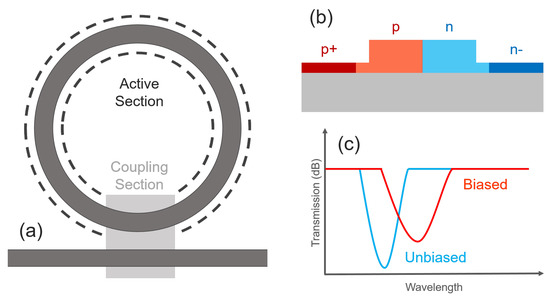
Figure 1. Ring modulator schematic with (a) Top down view showing the ring and the coupling waveguide (b) the diode embedded in the cross section (c) The effect biasing has on the transmission of the ring.
In operation, the primary benefits of the silicon ring modulator, also referred to as a micro-ring modulator (MRM) due to the devices’ small scale, are its small footprint, low power consumption, and narrow wavelength selectivity [18]. The challenges of silicon MRMs stems from silicon’s third order non linearity [19], which generates nonlinear effects, resulting in carrier [20] and thermal [21] induced optical bistabilities and self pulsation from these phenomena acting in competition to each other [22].
2.2. Mach-Zehnder Modulators (MZM)
Mach-Zehnder Modulators (MZMs) are another common optical modulator. MZMs are based on the original concept of a Mach-Zehnder Interferometer (MZI), which relies on separating light into two optical paths at some form of input coupler. the light travelling in one or both of these pathways can then have its phase modulated before the paths recombine and interference occurs. In the case of most semiconductors, the pathway arms of the MZM are usually equipped with phase modulators reliant on a drive voltage, with the voltage difference between full positive and negative interferences being denoted as the switching voltage; . The phase difference for this condition being a difference of between the phase of the light in the two arms.
MZMs can be noted for their high-contrast optical transmission without deterioration due to spectral broadening and frequency chirping [23][24][25][26]. In silicon photonics the monolothic integration of MZMs with other photonic components such as photodiodes is achievable with fabrication technologies to create integrated devices with small footprints [26][27][28]. In silicon MZMs the method of modulation relies on high speed refractive index modulation via free carrier plasma dispersion, or the carrier-refraction effect. This effect sees major usage in unstrained silicon and germanium where the Pockels effect; the voltage controlled phase delay in crystals, is not observed. Unstrained silicon is specified here as the Pockels effect has been recorded in strained silicon waveguides, although large voltages are required to achieve notable modulation [29]. Free carrier plasma dispersion has been used to design and model a wide range of silicon-based phase shifters [27]. Silicon optical modulators based on carrier dispersion effects typically use a PIN or PN diode structure across the optical waveguide to alter the density of free carriers available to interact with light within the guide [30]. Alternatively, demonstrations have been made which use the accumulation of free carriers around a thin dielectric layer in the waveguide [31]. PN junction based MZM modulators benefit from simple fabrication and high-speed performance but lack the modulation efficiency of the carrier injection and accumulation techniques.
Reed et al. presents a PN MZM with modulation efficiency ranging between 1.4 to 1.9 V/cm over reverse bias voltages between 0 and 6 V. An insertion loss of 5 dB was measured with 4dB being attributed to the phase modulator and 1 dB loss from the splitter and combiner. A speed of 52 Gb/s was demonstrated [32].
Xiao et al. demonstrates modulation speeds of up to 60 Gb/s in a silicon MZM using doping optimisation. A modulation efficiency of 2 V·cm was recorded with a maximum insertion loss of 3.5 dB [33].
2.3. Electro-Absorption Modulators (EAMs)
An electro-absorption modulator is a semiconductor PIN structure whose bandgap can be varied through the application of an external voltage, altering the devices absorption properties [34]. EAMs generally offer low drive voltages (∼2 V) and are cost effective in volume production. In effect, an EAM can be considered the opposite of a semiconductor laser diode. Both can be made on a semiconductor waveguide, forward bias producing photons and reverse bias absorbing them. Unfortunately this makes creating an effective pure silicon EAM incredibly challenging due to silicon’s indirect bandgap. The modulation in EAMs is achieved via the Quantum Confined Stark Effect (QCSE), which describes the change in light absorption spectrum of a quantum well material in response to an applied external electric field. The electric field causes electron states to shift to lower energies, and holes to higher energies.
Jeong et al. explores this challenge in a unique manner, incorporating homogeneous EAMs based on the aforementioned free carrier plasma dispersion effect [35]. Jeong utilises a Schottky diode as part of the EAM, achieving optical modulation by the intensity change of the light from the free carrier absorption to change the absorption coefficient, but not conventional interference effects. With this, 3 dB modulation depth was achieved at 6 from 1542 to 1558 nm for EAMs with length 500 m.
3. III–V Hybrid Modulators
The advent of heterogeneous PIC integration has introduced a plethora of possibilities for improvements to the optical components now available on the Silicon platform. Lasers have been demonstrated but are only one of the key components of a high speed optical transmitter, thus modulators must also be considered. Modulators formed from the integration of III–V materials and Silicon typically use metal oxide semiconductor modulators as they provide a good balance of modulation bandwidth and efficiency [36][37]. In the modulators presented, n-doped InGaAsP is bonded to a p-doped Si layer with an insulating layer separating the two. This results in a Semiconductor-Insulator-Semiconductor-CAPacitor (SISCAP) formation. The SIS configuration behaves like a capacitor with the semiconductors acting as the plates and the insulating layer acting as a capacitive area between. This structure causes charge to accumulate, which alters the refractive index.
In Drude’s model, the change in refractive index, n, caused by plasma dispersion is inversely proportional to the effective masses of holes and electrons [37]. The lighter n-doped III–V electrons result in a stronger electron-induced refractive index change when compared to Silicon [36]. Additionally, n-doped III–V materials provide a higher refractive index change per change in absorption coefficient, k [36]. The result is a phase modulator with reduced spurious intensity modulation. This behavior is also true for p-doped III–V materials for carrier concentrations above , and below this threshold p-doped Silicon provides a better ratio of n/ k [36][37]. A hybrid III–V/Si MOS modulator can merge the best of III–V and Silicon. Consequently, this approach offers modulators with up to 5 times better modulation efficiency, and a lower phase shifter loss than all-silicon MOS modulators [36][37].
Other methods of integrating Silicon and III–V MOS modulators exist. By implementing a III–V on Si MOS modulator in a ring coupled to a straight waveguide in a race-track pattern, the energy consumption of a 40-GHz modulator can be 3.7 times better than III–V on Si MZMs. This can be accomplished while maintaining a modulation efficiency of 0.064 V·cm. A schematic representation of this design is presented in Figure 2 [38]. The 100- m-long phase shifter section of the modulator is made using a thin aluminum oxide gate layer separating the n-doped III–V and the p-doped Silicon layers. A proof-of-concept, taper-less integration of a few tens of nanometers thick III–V layer with Silicon has been shown to reduce the footprint and loss of the device with-out compromising the modulation efficiency of the III–V on Si MOS capacitor [39].
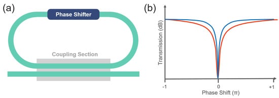
Figure 2. (a) Schematic of Si racetrack resonator with III–V/Si hybrid MOS optical phase shifter. (b) Numerically calculated transmission of a MZI modulator and a racetrack resonator.
Electro-absorption modulators (EAMs) have been reported by the bonding of III–V QWs with silicon [40][41]. These EAMs use a PIN structure. By applying a bias voltage, the absorption of the material’s quantum wells can be altered via the Quantum Con-fined Stark Effect (QCSE) [41]. A segmented electrode, comprising a low-impedance active modulation section cascaded by a high-impedance passive section, provides high-bandwidth operation while ensuring low reflection and good modulation efficiency [41]. An over 67 GHz bandwidth hybrid III–V on silicon EAM utilizing this method has been fabricated.In the O-band, this modulator has an insertion loss of 4.9 dB, and it shows >9 dB of dynamic ER for 50 Gb/s operation over a 16-km long optical fiber link. III–V on Si modulators have shown good modulation efficiency with low-loss, but so far devices of a notably higher speed (∼100 Gb/s) have yet to be experimentally verified.
References
- Wang, X.; Weigel, P.; Zhao, J.; Ruesing, M.; Mookherjea, S. Achieving beyond-100-GHz large-signal modula-tion bandwidth in hybrid silicon photonics Mach Zehnder modulators using thin film lithium niobate. APL Photonics 2019, 4, 096101.
- Bogaerts, W.; Taillaert, D.; Luyssaert, B.; Dumon, P.; Campenhout, J.; Bienstman, P.; Thourhout, D.; Baets, R.; Wiaux, V.; Beckx, S. Basic structures for photonic integrated circuits in Silicon-on-insulator. Opt. Express 2004, 12, 1583.
- Luyssaert, B.; Vandersteegen, P.; Taillaert, D.; Dumon, P.; Bogaerts, W.; Bienstman, P.; Van Thourhout, D.; Wiaux, V.; Beckx, S.; Baets, R. A compact photonic horizontal spot-size converter realized in silicon-on-insulator. IEEE Photonics Technol. Lett. 2005, 17, 73–75.
- Dumon, P.; Bogaerts, W.; Wiaux, V.; Wouters, J.; Beckx, S.; Van Campenhout, J.; Taillaert, D.; Luyssaert, B.; Bienstman, P.; Van Thourhout, D.; et al. Low-Loss SOI Photonic Wires and Ring Resonators Fabricated With Deep UV Lithography. IEEE Photonics Technol. Lett. 2004, 16, 1328–1330.
- Doylend, J.K.; Knights, A.P. The evolution of silicon photonics as an enabling technology for optical interconnec-tion. Laser Photonics Rev. 2012, 6, 504–525.
- Liu, A.; Jones, R.; Liao, L.; Samara-Rubio, D.; Rubin, D.; Cohen, O.; Nicolaescu, R.; Paniccia, M. A high-speed silicon optical modulator based on a metal-oxide-semiconductor capacitor. Nature 2004, 427, 615–618.
- Marris-Morini, D.; Le Roux, X.; Vivien, L.; Cassan, E.; Pascal, D.; Halbwax, M.; Maine, S.; Laval, S.; Fédéli, J.M.; Damlencourt, J.F. Optical modulation by carrier depletion in a silicon PIN diode. Opt. Express 2006, 14, 10838–10843.
- Xu, Q.; Schmidt, B.; Pradhan, S.; Lipson, M. Micrometrescale silicon electro-optic modulator. Nature 2005, 435, 325–327.
- Green, W.M.J.; Rooks, M.J.; Sekaric, L.; Vlasov, Y.A. Ultracompact, low RF power, 10 Gb/s silicon Mach-Zehnder modulator. Opt. Express 2007, 15, 17106–17113.
- Manipatruni, S.; Xu, Q.; Schmidt, B.; Shakya, J.; Lipson, M. High speed carrier injection 18 Gb/s silicon micro-ring electro-optic modulator. In Proceedings of the LEOS 2007-IEEE Lasers and Electro-Optics Society Annual Meeting Conference Proceedings Lasers and Electro-Optics Society, Lake Buena Vista, FL, USA, 21–25 October 2007; pp. 537–538.
- Liao, L.; Liu, A.; Rubin, D.; Basak, J.; Chetrit, Y.; Nguyen, H.; Cohen, R.; Izhaky, N.; Paniccia, M. 40 Gbit/s silicon optical modulator for highspeed applications. Electron. Lett. 2007, 43, 1196–1197.
- Liu, A.; Liao, L.; Rubin, D.; Basak, J.; Chetrit, Y.; Nguyen, H.; Cohen, R.; Izhaky, N.; Paniccia, M. Recent development in a high-speed silicon optical modulator based on reverse-biased pn diode in a silicon waveguide. Semicond. Sci. Technol. 2008, 23, 064001.
- Rosenberg, J.C.; Green, W.M.J.; Assefa, S.; Schow, C.L.; Rylyakov, A.V.; Gill, D.M.; Lee, B.G.; Jahnes, C.; Barwicz, T.; Shank, S.M.; et al. High-speed and low-power microring modulators for silicon photonics. In Proceedings of the IEEE Photonic Society 24th Annual Meeting, Arlington, VA, USA, 9–13 October 2011; pp. 256–257.
- Sun, J.; Kumar, R.; Sakib, M.; Driscoll, J.; Jayatilleka, H.; Rong, H. A 128 Gb/s PAM4 Silicon Microring Modulator With Integrated Thermo-Optic Resonance Tuning. J. Light. Technol. 2019, 37, 110–115.
- Bogaerts, W.; De Heyn, P.; Van Vaerenbergh, T.; De Vos, K.; Kumar Selvaraja, S.; Claes, T.; Dumon, P.; Bienstman, P.; Van Thourhout, D.; Baets, R. Silicon microring resonators. Laser Photonics Rev. 2011, 6, 47–73.
- Soref, R.; Bennett, B. Electrooptical effects in silicon. IEEE J. Quantum Electron. 1987, 23, 123–129.
- Timurdogan, E.; Sorace-Agaskar, C.M.; Sun, J.; Hosseini, E.S.; Biberman, A.; Watts, M.R. An ultralow power athermal silicon modulator. Nat. Commun. 2014, 5, 4008.
- Preston, K.; Sherwood-Droz, N.; Levy, J.S.; Lipson, M. Performance guidelines for WDM interconnects based on silicon microring resonators. In Proceedings of the CLEO: 2011-Laser Science to Photonic Applications, Baltimore, MD, USA, 1–6 May 2011; pp. 1–2.
- Dinu, M.; Quochi, F.; Garcia, H. Third-order nonlinearities in silicon at telecom wavelengths. Appl. Phys. Lett. 2003, 82, 2954–2956.
- Almeida, V.R.; Lipson, M. Optical bistability on a silicon chip. Opt. Lett. 2004, 29, 2387–2389.
- Xu, Q.; Lipson, M. Carrier-induced optical bistability in silicon ring resonators. Opt. Lett. 2006, 31, 341–343.
- Johnson, T.J.; Borselli, M.; Painter, O. Self-induced optical modulation of the transmission through a high-Q silicon microdisk resonator. Opt. Express 2006, 14, 817–831.
- Koyama, F.; Iga, K. Frequency chirping in external modulators. J. Light. Technol. 1988, 6, 87–93.
- Gnauck, A.H.; Winzer, P.J. Optical phase-shift-keyed transmission. J. Light. Technol. 2005, 23, 115–130.
- Winzer, P.J.; Essiambre, R. Advanced Optical Modulation Formats. Proc. IEEE 2006, 94, 952–985.
- Kikuchi, K. Coherent transmission systems. In Proceedings of the 2008 34th European Conference on Optical Communication, Brussels, Belgium, 21–25 September 2008; pp. 1–39.
- Reed, G.T.; Mashanovich, G.; Gardes, F.Y.; Thomson, D.J. Silicon optical modulators. Nature Photonics 2010, 4, 518–526.
- Liow, T.Y.; Ang, K.W.; Fang, Q.; Song, J.F.; Xiong, Y.Z.; Yu, M.B.; Lo, G.Q.; Kwong, D.L. Silicon Modulators and Germanium Photodetectors on SOI: Monolithic Integration, Compatibility, and Performance Optimization. IEEE J. Sel. Top. Quantum Electron. 2010, 16, 307–315.
- Damas, P.; Le Roux, X.; Le Bourdais, D.; Cassan, E.; Marris-Morini, D.; Izard, N.; Maroutian, T.; Lecoeur, P.; Vivien, L. Pockels effect study in Strained Silicon Mach-Zenhder Interferometer. In Proceedings of the 11th International Conference on Group IV Photonics (GFP), Paris, France, 27–29 August 2014; pp. 243–244.
- Reed, G.T.; Mashanovich, G.Z.; Gardes, F.Y.; Nedeljkovic, M.; Hu, Y.; Thomson, D.J.; Li, K.; Wilson, P.R.; Chen, S.W.; Hsu, S.S. Recent breakthroughs in carrier depletion based silicon optical modulators. Nanophotonics 2014, 3, 229–245.
- Webster, M.; Gothoskar, P.; Patel, V.; Piede, D.; Anderson, S.; Tummidi, R.; Adams, D.; Appel, C.; Metz, P.; Sunder, S.; et al. An efficient MOS-capacitor based silicon modulator and CMOS drivers for optical transmitters. In Proceedings of the 11th International Conference on Group IV Photonics (GFP), Paris, France, 27–29 August 2014; pp. 1–2.
- Reed, G.; Thomson, D.; Gardes, F.; Hu, Y.; Fedeli, J.; Mashanovich, G. High-speed carrier-depletion silicon Mach-Zehnder optical modulators with lateral PN junctions. Front. Phys. 2014, 2, 77.
- Xiao, X.; Xu, H.; Li, X.; Li, Z.; Chu, T.; Yu, Y.; Yu, J. High-speed, low-loss silicon Mach–Zehnder modulators with doping optimization. Opt. Express 2013, 21, 4116–4125.
- Ackermann, D.A.; Johnson, J.E.; Ketelsen, L.J.P.; Eng, L.E.; Kiely, P.A.; Mason, T.G.B. Telecommunication lasers. In Optical Fiber Telecommunications IV; Kaminow, I., Li, T., Eds.; Academic Press: New York, NY, USA, 2002; pp. 587–665.
- Jeong, U.; Lee, D.H.; Lee, K.; Park, J.H. Monolithic 1 × 8 DWDM Silicon Optical Transmitter Using an Arrayed-Waveguide Grating and Electro-Absorption Modulators for Switch Fabrics in Intra-Data-Center Interconnects. Micromachines 2020, 11, 991.
- Li, Q.; Ho, C.P.; Takagi, S.; Takenaka, M. Efficient optical modulator by reverse-biased III–V/ Si hybrid MOS capacitor based on FK effect and carrier depletion. In Proceedings of the 2019 Optical Fiber Communications Conference and Exhibition (OFC), San Diego, CA, USA, 3–7 March 2019.
- Li, Q.; Ho, C.P.; Takagi, S.; Takenaka, M. Optical phase modulators based on reverse-biased III–V/Si hybrid metal-oxide-semiconductor capacitors. IEEE Photonics Technol. Lett. 2020, 32, 345–348.
- Li, Q.; Ho, C.; Takagi, S.; Takenaka, M. Si racetrack modulator with III–V/Si hybrid MOS optical phase shifter. In Proceedings of the 45th European Conference on Optical Communication (ECOC 2019), Dublin, Ireland, 22–26 September 2019.
- Ohno, S.; Li, Q.; Sekine, N.; Fujikata, J.; Noguchi, M.; Takahashi, S.; Toprasertpong, K.; Takagi, S.; Takenaka, M. Taper-less III–V/Si hybrid MOS optical phase shifter using ultrathin InP membrane. In Proceedings of the Optical Fiber Communication Conference, San Diego, CA, USA, 8–12 March 2020.
- Tang, Y.; Peters, J.D.; Bowers, J.E. Over 67 GHz bandwidth hybrid silicon electro-absorption modulator with asymmetric segmented electrode for 1.3 μm transmission. Opt. Express 2012, 20, 11529–11535.
- Tang, Y.; Chen, H.W.; Jain, S.; Peters, J.D.; Westergren, U.; Bowers, J.E. 50 Gb/s hybrid silicon traveling-wave electro-absorption modulator. Opt. Express 2011, 19, 5811–5816.
More
Information
Subjects:
Optics
Contributor
MDPI registered users' name will be linked to their SciProfiles pages. To register with us, please refer to https://encyclopedia.pub/register
:
View Times:
5.6K
Revisions:
3 times
(View History)
Update Date:
08 Feb 2022
Table of Contents


Notice
You are not a member of the advisory board for this topic. If you want to update advisory board member profile, please contact office@encyclopedia.pub.
OK
Confirm
Only members of the Encyclopedia advisory board for this topic are allowed to note entries. Would you like to become an advisory board member of the Encyclopedia?
Yes
No
${ textCharacter }/${ maxCharacter }
Submit
Cancel
Back
Comments
${ item }
|
${ item.createdUser.fullName }
${ item.createdAt }
${ item.vote }
${ item.reply }
Delete
${ reply.createdUser.fullName }
${ reply.createdAt }
${ reply.vote }
Delete
There is no reply to this comment~
${ item.replyTextCharacter }/${ item.replyMaxCharacter }
Submit
Cancel
More
No more~
There is no comment~
${ textCharacter }/${ maxCharacter }
Submit
Cancel
${ selectedItem.replyTextCharacter }/${ selectedItem.replyMaxCharacter }
Submit
Cancel
Confirm
Are you sure to Delete?
Yes
No