Your browser does not fully support modern features. Please upgrade for a smoother experience.
Submitted Successfully!
 +1 credit
Thank you for your contribution! You can also upload a video entry or images related to this topic.
For video creation, please contact our Academic Video Service.
Video Upload Options
We provide professional Academic Video Service to translate complex research into visually appealing presentations. Would you like to try it?
Cite
If you have any further questions, please contact Encyclopedia Editorial Office.
Chen, W. GaN-Based Resonant-Cavity Light-Emitting Diodes Grown on Si. Encyclopedia. Available online: https://encyclopedia.pub/entry/18284 (accessed on 13 June 2026).
Chen W. GaN-Based Resonant-Cavity Light-Emitting Diodes Grown on Si. Encyclopedia. Available at: https://encyclopedia.pub/entry/18284. Accessed June 13, 2026.
Chen, Wen. "GaN-Based Resonant-Cavity Light-Emitting Diodes Grown on Si" Encyclopedia, https://encyclopedia.pub/entry/18284 (accessed June 13, 2026).
Chen, W. (2022, January 15). GaN-Based Resonant-Cavity Light-Emitting Diodes Grown on Si. In Encyclopedia. https://encyclopedia.pub/entry/18284
Chen, Wen. "GaN-Based Resonant-Cavity Light-Emitting Diodes Grown on Si." Encyclopedia. Web. 15 January, 2022.
Copy Citation
GaN-on-Si resonant-cavity light-emitting diodes (RCLEDs) have been successfully fabricated through wafer bonding and Si substrate removal.
GaN-on-Si
resonant-cavity light-emitting diode
chemical-mechanical polishing
visible light communications
1. Introduction
GaN-based resonant-cavity light-emitting diodes (RCLEDs) with narrow spectral width, stable peak wavelength, superior directionality, and high output-coupling efficiency [1][2][3][4] have shown great potential applications in various fields, such as line-of-sight visible light communications (VLCs), plastic optical fiber-based networks, optical scanners, speckle-free illumination, printers, and displays [5][6][7][8].
Up to now, there have been no GaN-based RCLED products. The main bottleneck is that most GaN-based RCLEDs are grown on sapphire substrates, resulting in several issues. For GaN-based RCLEDs with hybrid distributed Bragg reflectors (DBRs), about 40 pairs of GaN/AlGaN or GaN/InAlN DBRs are usually grown underneath the quantum wells (QWs) [9][10][11][12], which may not only induce high tensile stress and even micro-cracks, but also increase the dislocation density, seriously reducing the internal quantum efficiency [13]. For GaN-based RCLEDs with double-sided dielectric DBRs, the laser lift-off process is usually used to remove the sapphire substrates [14][15], which often causes high stress and even cracks, greatly affecting the device performance and yield. Compared with sapphire substrates, Si substrates can be easily removed by wet chemical etching without any damage. Si substrates also have unique advantages in wafer size and material cost, as well as the use of depreciated automation processing lines [16]. Lastly, Si substrates match with the conductive Si submount in the coefficient of thermal expansion, which can greatly reduce the stress in the bonding process and hence improve the device performance and yield. Therefore, replacing the small-sized (≤6 inches) sapphire substrates with large-diameter (up to 20 inches) cost-effective Si substrates is expected to greatly slash the device fabrication cost, and increase the device performance and yield, ultimately realizing the mass production of GaN-based RCLEDs.
2. GaN-Based Resonant-Cavity Light-Emitting Diodes Grown on Si
A rough surface will cause a large optical scattering loss, and hence ultimately affect the quality of the resonant cavity. Therefore, it is necessary to obtain a flat morphology to deposit dielectric DBRs. However, the Cl-based plasmas in the ICP etching often cause an uneven etching, especially for high-Al-composition AlGaN materials, which increases the surface roughness [17]. After removing the AlN/AlGaN multilayer buffer by ICP etching, the surface roughness of the N-face n-GaN was about 3.56 nm for a scan area of 5 μm × 5 μm, as shown in Figure 1a. To smooth the surface morphology, a CMP technology with silica solution was developed. The alkaline silica solution could preliminarily corrode and soften the N-face n-GaN surface, and then the silica nanoparticles in the solution could polish and smooth the N-face n-GaN surface [18]. Figure 1b shows the surface morphology of N-face n-GaN after polishing 1200 nm with the silica solution for 30 min. The roughness of a scan area of 5 μm × 5 μm was greatly reduced from 3.56 to 0.24 nm, which was further evidenced by the cross-sectional STEM image of the as-fabricated device as shown in Figure 1c. This surface smoothness was comparable to that of the as-grown Ga-face GaN, and paved the way for the deposition of high-quality n-side dielectric DBRs [19]. As a result, the 11.5-pair TiO2/SiO2 n-DBRs showed a peak reflectivity of 99% at 405 nm with a large stop-band of about 80 nm, as shown in Figure 1d, which is almost equal to that of the 12.5-pair p-DBRs (99.5%).
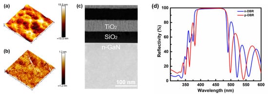
Figure 1. AFM images of the N-face n-GaN surface (a) before and (b) after the CMP with silica solution showing a scan area of 5 × 5 μm2. (c) Cross-sectional STEM image of the interface between the N-face n-GaN and the n-side DBR. (d) Experimental reflectance spectra of the n-DBR and p-DBR.
Figure 2a presents the measured light–current–voltage (L–I–V) plots. The I-V curve of the as-fabricated RCLED exhibited a turn-on voltage of approximately 3 V. Above the turn-on voltage, the current density gradually increased with voltage. The inset of Figure 2a presents the leakage current under a reverse bias. At −5 V, the reverse leakage current was as low as 0.34 nA, which indicates that the fluoride ion implantation effectively insulated the devices. The fluoride ion with a very strong electronegativity could not only trap free electrons, but also reduce the carrier density by host-type defects at ultra-deep energy levels, ultimately leading to the insulation of the devices [20]. Figure 2b shows the EL spectrum of the as-fabricated RCLED at an injection current of 7 mA. Compared with conventional LEDs, the FWHM of the EL spectrum was reduced from about 15.5 to 10.6 nm due to the resonant cavity effect [21]. On the other hand, as shown in Figure 2b, the EL spectrum of the RCLED was periodically modulated by the Fabry–Pérot (F–P) cavity formed by the double-sided dielectric DBRs [22], and showed several narrow resonant peaks with a spacing of about 4 nm. This was mainly due to the interference effect as light bounced back and forth between the double-sided DBRs until the constructive conditions achieved allowed the cavity modes to escape from the LEDs [23]. Based on the analysis method described in [7], the inset of Figure 2b shows a dominant resonant peak at a wavelength of about 405 nm with a FWHM of approximately 1 nm, corresponding to a quality factor of 405. For the as-fabricated GaN-based RCLED, with a mode spacing of 4 nm, the cavity length of the RCLED was calculated as 5.05 μm at the peak wavelength of λ0 = 405 nm [24][25]. This value was larger than the total thickness of the GaN-based epilayers (4.2 μm) measured by STEM, which was mainly because the effective resonant cavity was composed of not only the remaining GaN-based epilayers but also the double-sided DBR mirrors. For the as-fabricated GaN-based RCLED, part of the optical field would penetrate into the double-sided dielectric DBRs, which contributed to the increased effective cavity length [23]. Figure 2c presents the peak wavelength of the device under various injection currents. For the GaN-based emitter with similar epitaxial structure [26], the peak wavelength of the EL spectrum was blue-shifted from 416.2 to 412.7 nm as the injection current density was increased from 1.5 to 4.7 kA/cm2, which was mainly due to the screened quantum-confined Stark effect. In contrast, for the as-fabricated GaN-based RCLED, the peak wavelength only decreased from 405.2 to 404.7 nm while the injection current density increased from 1.45 to 4.36 kA/cm2. Thanks to the short cavity formed by the double-sided DBRs, the GaN-based RCLED showed a much more stable peak wavelength.
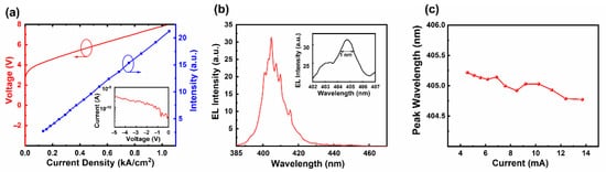
Figure 2. (a) Measured L–I–V characteristics of the as-fabricated GaN-based RCLED, and the inset showing leakage current under a reverse bias. (b) EL spectrum of the RCLED at an injection current of 7 mA, and the inset showing the dominant cavity mode with a linewidth of approximately 1 nm. The silicon detector was located 1 cm directly above the device and collected only a portion of the output power. (c) The peak wavelength of RCLED at various injection currents.
Figure 3a,b shows the top-view SEM and the light-up images of the as-fabricated GaN-based RCLED, respectively. It can be clearly seen that the circular shape of the 20-μm-diameter device was well preserved, and uniform luminescence was achieved by using a 30-nm-thick ITO current spreading layer. In Figure 3b, the peripheral blue luminescence was mainly due to the light scattering by the peripheral of the n-side DBRs.
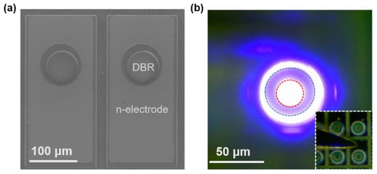
Figure 3. (a) Top-view SEM and (b) light-up images of the as-fabricated GaN-based RCLED with a diameter of 20 μm. In (b), the injection current was 2 mA, and the red and blue circles show the sizes of the current aperture and the n-side DBR, respectively. The inset shows the optical microscopy image of the RCLED.
The high-speed data transmission feasibility of the as-fabricated GaN-based RCLED was examined by a free space visible light communication (VLC) measurement system. Figure 4a shows the open eye diagram of the as-fabricated GaN-based RCLED measured at 150 Mbps, and Figure 4b shows the waveform diagram of optical signal and electrical signal. It can be clearly seen that the optical signal matches with the electrical signal very well, showing a good transmission feasibility. It should be clearly noted that the transmission rate of 150 Mbps was the maximum value of the detection system, and we believe that the actual maximum transmission rate could be even higher.
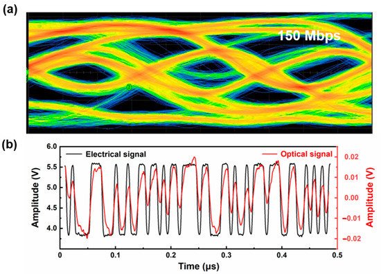
Figure 4. (a) Measured eye diagram of the as-fabricated GaN-based RCLED at a transmission rate of 150 Mbps. (b) The waveform diagram of optical signal and electrical signal at a transmission rate of 150 Mbps.
References
- Wirth, R.; Karnutsch, C.; Kugler, S.; Streubel, K. High-efficiency resonant-cavity LEDs emitting at 650 nm. IEEE Photonics Technol. Lett. 2001, 13, 421–423.
- Huang, S.Y.; Horng, R.H.; Liu, P.L.; Wu, J.Y.; Wu, H.W.; Wuu, D.S. Thermal Stability Improvement of Vertical Conducting Green Resonant-Cavity Light-Emitting Diodes on Copper Substrates. IEEE Photonics Technol. Lett. 2008, 20, 797–799.
- Chen, J.R.; Ko, T.S.; Lu, T.S.; Chang, Y.A.; Kuo, H.C.; Kuo, Y.K.; Tsai, J.K.; Laih, L.W.; Wang, S.C. Fabrication and Characterization of Temperature Insensitive 660-nm Resonant-Cavity LEDs. J. Lightwave Technol. 2008, 26, 1891–1900.
- Yeh, P.S.; Yu, M.C.; Lin, J.H.; Huang, C.C.; Liao, Y.C.; Lin, D.W.; Fan, J.R.; Kuo, H.C. GaN-Based Resonant-Cavity LEDs Featuring a Si-Diffusion-Defined Current Blocking Layer. IEEE Photonics Technol. Lett. 2014, 26, 2488–2491.
- Kim, J.H.; Lee, S.J.; Park, S.H. InGaN-Based Resonant-Cavity Light-Emitting Diodes with a ZrO2/SiO2 Distributed Bragg Reflector and Metal Reflector. Jpn. J. Appl. Phys. 2010, 49, 122102.
- Cai, W.; Yuan, J.L.; Ni, S.Y.; Shi, Z.; Zhou, W.D.; Liu, Y.H.; Wang, Y.J.; Amano, H. GaN-on-Si resonant-cavity light-emitting diode incorporating top and bottom dielectric distributed Bragg reflectors. Appl. Phys. Express 2019, 12, 032004.
- Huang, S.Y.; Horng, R.H.; Wuu, D.S.; Wang, W.K.; Yu, T.E.; Lin, P.R.; Juang, F.S. Effects of Transparent Conductive Layers on Characteristics of InGaN-Based Green Resonant-Cavity Light-Emitting Diodes. Jpn. J. Appl. Phys. 2007, 46, 3416–3419.
- Huang, S.Y.; Horng, R.H.; Shi, J.W.; Kuo, H.C.; Wuu, D.S. High-Performance InGaN-Based Green Resonant-Cavity Light-Emitting Diodes for Plastic Optical Fiber Applications. J. Lightwave Technol. 2009, 27, 4084–4094.
- Moudakir, T.; Genty, F.; Kunzer, M.; Borner, P.; Passow, T.; Suresh, S.; Patriarche, G.; Kohler, K.; Pletschen, W.; Wagner, J.; et al. Design, Fabrication, and Characterization of Near-Milliwatt-Power RCLEDs Emitting at 390 nm. IEEE Photonics J. 2013, 5, 8400709.
- Inaba, T.; Tatebayashi, J.; Shiomi, K.; Timmerman, D.; Ichikawa, S.; Fujiwara, Y. GaN:Eu, O-Based Resonant-Cavity Light Emitting Diodes with Conductive AlInN/GaN Distributed Bragg Reflectors. ACS Appl. Electron. Mater. 2020, 2, 732–738.
- Berger, C.; Dadgar, A.; Bläsing, J.; Franke, A.; Hempel, T.; Goldhahn, R.; Christen, J.; Krost, A. Growth of AlInN/AlGaN distributed Bragg reflectors for high quality microcavities. Phys. Status Solidi C 2012, 9, 1253–1258.
- Butté, R.; Feltin, E.; Dorsaz, J.; Christmann, G.; Carlin, J.F.; Grandjean, N.; Ilegems, M. Recent Progress in the Growth of Highly Reflective Nitride-Based Distributed Bragg Reflectors and Their Use in Microcavities. Jpn. J. Appl. Phys. 2005, 44, 7207–7216.
- Khan, M.A.; Kuznia, J.N.; Van Hove, J.M.; Olson, D.T. Reflective filters based on single-crystal GaN/AlxGa1−xN multilayers deposited using low-pressure metalorganic chemical vapor deposition. Appl. Phys. Lett. 1991, 59, 1449–1451.
- Hu, X.L.; Liu, W.J.; Weng, G.E.; Zhang, J.Y.; Lv, X.Q.; Liang, M.M.; Chen, M.; Huang, H.J.; Ying, L.Y.; Zhang, B.P. Fabrication and Characterization of High-Quality Factor GaN-Based Resonant-Cavity Blue Light-Emitting Diodes. IEEE Photonics Technol. Lett. 2012, 24, 1472–1474.
- Hu, X.L.; Zhang, J.Y.; Liu, W.J.; Chen, M.; Zhang, B.P.; Xu, B.S.; Wang, Q.M. Resonant-cavity blue light-emitting diodes fabricated by two-step substrate transfer technique. Electron. Lett. 2011, 47, 986–988.
- Feng, M.X.; Li, Z.C.; Wang, J.; Zhou, R.; Sun, Q.; Sun, X.J.; Li, D.B.; Gao, H.W.; Zhou, Y.; Zhang, S.M.; et al. Room-Temperature Electrically Injected AlGaN-Based near-Ultraviolet Laser Grown on Si. ACS Photonics 2018, 5, 699–704.
- Shah, A.P.; Laskar, M.R.; Azizur Rahman, A.; Gokhale, M.R.; Bhattacharya, A. Inductively coupled plasma–reactive ion etching of c- and a-plane AlGaN over the entire Al composition range: Effect of BCl3 pretreatment in Cl2/Ar plasma chemistry. J. Vac. Sci. Technol. 2013, 31, 061305.
- Tavernier, P.R.; Margalith, T.; Coldren, L.A.; DenBaars, S.P.; Clarke, D.R. Chemical Mechanical Polishing of Gallium Nitride. Electrochem. Solid-State Lett. 2002, 5, G61–G64.
- Sun, Q.; Suk Cho, Y.; Kong, B.H.; Koun Cho, H.; Shine Ko, T.; Yerino, C.D.; Lee, I.-H.; Han, J. N-face GaN growth on c-plane sapphire by metalorganic chemical vapor deposition. J. Cryst. Growth 2009, 311, 2948–2952.
- Liu, Z.; Wang, J.; Gu, H.; Zhang, Y.; Wang, W.; Xiong, R.; Xu, K. High-voltage vertical GaN-on-GaN Schottky barrier diode using fluorine ion implantation treatment. AIP Adv. 2019, 9, 055016.
- Li, Z.H.; Yang, Z.J.; Yu, T.J.; Zhang, G.Y.; Feng, Y.C.; Niu, H.B. Properties of InGaN violet-LED structure. In Proceedings of the Fifth International Conference on Thin Film Physics and Applications, 31 May–2 June 2004; Volume 5774, pp. 381–384.
- Song, Y.K.; Diagne, M.; Zhou, H.; Nurmikko, A.V.; Schneider, R.P.; Takeuchi, T. Resonant-cavity InGaN quantum-well blue light-emitting diodes. Appl. Phys. Lett. 2000, 77, 1744.
- Tsai, C.L.; Yen, C.T.; Huang, W.J.; Xu, Z.F.; Ko, S.C. InGaN-Based Resonant-Cavity Light-Emitting Diodes Fabricated With a TaO2/SiO2 Distributed Bragg Reflector and Metal Reflector for Visible Light Communications. J. Disp. Technol. 2013, 9, 365–370.
- Yu, G.; Wang, G.; Ishikawa, H.; Umeno, M.; Soga, T.; Egawa, T.; Watanabe, J.; Jimbo, T. Optical properties of wurtzite structure GaN on sapphire around fundamental absorption edge (0.78–4.77 eV) by spectroscopic ellipsometry and the optical transmission method. Appl. Phys. Lett. 1997, 70, 3209–3211.
- Schwarz, U.T.; Sturm, E.; Wegscheider, W.; Kümmler, V.; Lell, A.; Härle, V. Optical gain, carrier-induced phase shift, and linewidth enhancement factor in InGaN quantum well lasers. Appl. Phys. Lett. 2003, 83, 4095–4097.
- Sun, Y.; Zhou, K.; Sun, Q.; Liu, J.P.; Feng, M.X.; Li, Z.C.; Zhou, Y.; Zhang, L.Q.; Li, D.Y.; Zhang, S.M.; et al. Room-temperature continuous-wave electrically injected InGaN-based laser directly grown on Si. Nat. Photonics 2016, 10, 595–599.
More
Information
Subjects:
Optics
Contributor
MDPI registered users' name will be linked to their SciProfiles pages. To register with us, please refer to https://encyclopedia.pub/register
:
View Times:
1.0K
Revisions:
2 times
(View History)
Update Date:
17 Jan 2022
Table of Contents


Notice
You are not a member of the advisory board for this topic. If you want to update advisory board member profile, please contact office@encyclopedia.pub.
OK
Confirm
Only members of the Encyclopedia advisory board for this topic are allowed to note entries. Would you like to become an advisory board member of the Encyclopedia?
Yes
No
${ textCharacter }/${ maxCharacter }
Submit
Cancel
Back
Comments
${ item }
|
${ item.createdUser.fullName }
${ item.createdAt }
${ item.vote }
${ item.reply }
Delete
${ reply.createdUser.fullName }
${ reply.createdAt }
${ reply.vote }
Delete
There is no reply to this comment~
${ item.replyTextCharacter }/${ item.replyMaxCharacter }
Submit
Cancel
More
No more~
There is no comment~
${ textCharacter }/${ maxCharacter }
Submit
Cancel
${ selectedItem.replyTextCharacter }/${ selectedItem.replyMaxCharacter }
Submit
Cancel
Confirm
Are you sure to Delete?
Yes
No