Your browser does not fully support modern features. Please upgrade for a smoother experience.
Submitted Successfully!
 +1 credit
Thank you for your contribution! You can also upload a video entry or images related to this topic.
For video creation, please contact our Academic Video Service.
| Version | Summary | Created by | Modification | Content Size | Created at | Operation |
|---|---|---|---|---|---|---|
| 1 | Han Eol Lee | + 2010 word(s) | 2010 | 2021-11-03 03:30:50 | | | |
| 2 | Camila Xu | Meta information modification | 2010 | 2021-11-05 01:41:34 | | |
Video Upload Options
We provide professional Academic Video Service to translate complex research into visually appealing presentations. Would you like to try it?
Cite
If you have any further questions, please contact Encyclopedia Editorial Office.
Lee, H.E. Flexible Micro Light-Emitting Diodes. Encyclopedia. Available online: https://encyclopedia.pub/entry/15703 (accessed on 28 July 2026).
Lee HE. Flexible Micro Light-Emitting Diodes. Encyclopedia. Available at: https://encyclopedia.pub/entry/15703. Accessed July 28, 2026.
Lee, Han Eol. "Flexible Micro Light-Emitting Diodes" Encyclopedia, https://encyclopedia.pub/entry/15703 (accessed July 28, 2026).
Lee, H.E. (2021, November 04). Flexible Micro Light-Emitting Diodes. In Encyclopedia. https://encyclopedia.pub/entry/15703
Lee, Han Eol. "Flexible Micro Light-Emitting Diodes." Encyclopedia. Web. 04 November, 2021.
Copy Citation
The μLED has been spotlighted as a novel fusion technology of information technology (IT) and nanotechnology (NT) and is proposed as the next-generation light source to solve numerous problems of existing OLED and QLED displays (e.g., afterimage, burn-in effect, heat/water instability, and slow response time).
μLED
Internet of Things
bulk LED
1. Introduction
With the beginning of the Internet of Things (IoT) era, novel methods for efficient information utilization to handle and share various kinds of information in daily life have been discussed [1][2][3][4][5][6][7][8][9][10][11][12][13][14]. According to these requirements, academia and industries are attempting to narrow the physical/psychological distance between users and information, which is expected to be enabled by developing and commercializing various smart devices, including smart watches, home appliances, cell phones, and glasses. In other words, there has been a considerable amount of effort to realize a human–machine interface (HMI) in various aspects [15][16][17][18][19].
Since modern people are accustomed to lots of information, the desire to check their body/disease information in order to easily monitor and treat them has increased. These needs have been directly applied to newly develop smart devices. For example, smart devices can monitor various biometric information, such as pulse, heartbeat, and oxygen saturation, and then analyze living patterns (e.g., exercise and sleep and) in real time, helping to manage personal health [20][21][22][23][24][25]. For sustainable health monitoring and treatment, users have to continuously carry or wear the smart device obtaining information. However, these devices still have a critical limitation: huge equipment size, which is due to the intrinsic large volume of components, including batteries, circuits, and displays. In this regard, healthcare devices with a new form factor have been spotlighted, creating competition for the leading position in this fierce industry.
Recently, light-induced monitoring and treatment have attracted a lot of attention because of their biocompatibility, high therapeutic efficiency, and less-invasive process [26][27][28][29][30]. Since light-based healthcare devices collect accurate, vital information or efficiently cure physical illnesses without tissue damage, numerous medical teams are actively utilizing lasers or bulk light-emitting diodes (LEDs) as therapeutic equipment. However, this equipment has some drawbacks, such as its huge size, low power efficiency, high cost, and difficulty of frequent uses, as shown in Figure 1.
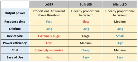
Figure 1. Comparison of LASER, bulk LED, and μLED as a light source for biomedical applications (red: disadvantages, blue: advantages).
Therefore, several researchers around the world have tried to miniaturize these phototherapy devices to ensure user-friendliness, convenience, and sustainable use. Among various light sources such as organic LEDs (OLEDs), quantum dot (QD)-based LEDs (QLEDs), and bulk LEDs, compound semiconductor-based inorganic microLEDs (μLEDs) have been considered as a next generation novel light source for biomedical applications because of their high brightness, superior power efficiency, fast response time, and excellent stability [7][10][17][31][32][33][34][35]. In particular, μLEDs can be easily manufactured into free form factor optoelectronic devices due to their ultra-small size, showing the advantage of flexibility and the possibility for wearable biomedical applications. According to these advantages, the μLEDs have been applied to various bio-applications such as optogenetics, vital monitoring, and hair loss treatment.
2. Flexible Micro Light-Emitting Diodes
The μLED has been spotlighted as a novel fusion technology of information technology (IT) and nanotechnology (NT) and is proposed as the next-generation light source to solve numerous problems of existing OLED and QLED displays (e.g., afterimage, burn-in effect, heat/water instability, and slow response time). Figure 2 shows a comparison table among QLED, OLED, and μLED displays in terms of their emission type, thickness, optical property, lifetime, and cost. The μLEDs are self-emissive light sources with high brightness and a longer lifetime than OLED and QLED, and display excellent image quality. In particular, μLEDs of extremely small size (width from 10 to 100 μm and thickness under 5 μm) have superior optical/electrical properties, such as excellent luminescence efficiency over 100 lm W−1, strong illumination over 105 cd m−2, high color contrast, and superior power efficiency.
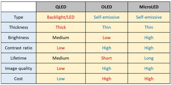
Figure 2. Comparison of QLED, OLED, and μLED display in terms of structure, optical/electrical properties, lifetime, and cost (red: disadvantages, blue: advantages).
Therefore, in the display industry, it is predicted that high-performance μLEDs will even enter fine-pitch display fields that are dominated by OLEDs and QLEDs, as shown in Figure 3. Despite several advantages of μLEDs, there are still some challenges in realizing commercialization, such as efficient packaging, chip structure innovation, and development of a new transfer methodology.
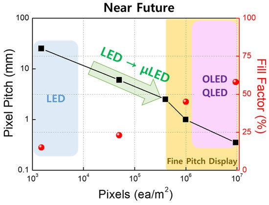
Figure 3. Development prospect of light sources as display components.
First, flexible μLEDs are fabricated as follows [11][35][36][37][38][39]: III-V compound semiconductor layers are grown by metalorganic chemical vapor deposition (MOCVD), metalorganic vapor-phase epitaxy (MOVPE), or molecular beam epitaxy (MBE) on the mother substrate (e.g., silicon, GaAs, and sapphire), forming a thin-film LED structure with a p-type material, a multi quantum well (MQW), and an n-type material. The epitaxial layers are etched into numerous microscale chips through micro-electromechanical systems (MEMS) processes. The LEDs on the mother substrate are selectively peeled off and placed into a specific position on a target substrate. Finally, the μLEDs are electrically connected and packaged for passivating the device from environmental stresses.
The μLEDs can typically be divided into three types (Figure 4). There are fully packaged bulk LEDs, as well as lateral- and vertical-structured μLEDs, which are made by III-V or III-N compound semiconductors on epitaxial substrate (e.g., III-V: GaAs; III-N: Si, SiC, and sapphire). They have different characteristics in thermal, electrical, and optical properties, resulting from structural differences of bulk/thin-film and electrode location. Lateral μLEDs have a long current path of about 50~100 μm between electrodes, whereas vertical μLEDs have a short current path under 5 μm, inducing negligible Joule heating during device operation. Thanks to this structural advantage, vertical-structured microLEDs have various superiorities compared to others, including a small size, a fast/cheap process, superior electrical/thermal properties, and simple wiring. Particularly, vertical-structured μLEDs with low heating are most suitable to realize biomedical applications due to their thermally noninvasive property.
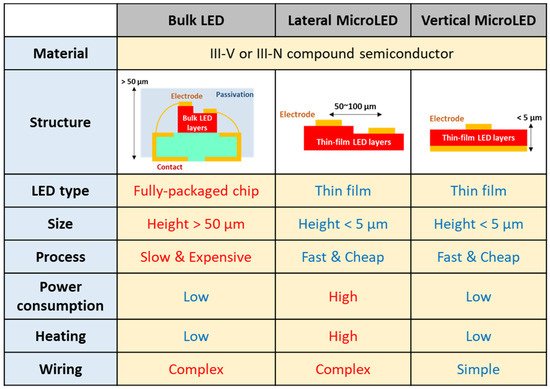
Figure 4. Comparison of bulk LED, lateral-, and vertical-structured μLEDs; red: disadvantages, blue: advantages).
As mentioned above, the processes, i.e., the transfer technology of numerous μLED chips from the mother wafer to the target substrate, are the most important factors for developing μLED-based electronic systems, such as displays, biomedical therapeutic devices, and healthcare sensors. Since the transfer efficiency is directly related to the device yield, manufacturing time, and unit cost, several researchers around the world have attempted to transfer thin-film μLED chips through various methods. The polydimethylsiloxane (PDMS)-based pick-and-place method was the most widely used for μLED transfer. The μLED chips were attached to sticky PDMS by van der Waals adhesive force and released onto the adhesive-coated target substrate. Furthermore, although various approaches, such as electrostatic or electromagnetic force-based transfer, were suggested as new transfer methods, they still had many problems, including thermal/electrical damage to the LED layers, slow transfer speed, and difficulty in large-area processing. Recently, novel technology was proposed by using an anisotropic conductive film (ACF) [32][35][40]. Thin-film μLEDs were simultaneously attached and packaged with the target substrate through ACF by applying heat and pressure. The ACF-based transfer was performed with a rapid process speed, high yield, and large-area transfer, enabling electrical connection with complicated electrodes at the same time as the μLED transfer.
Figure 5a shows a self-powered flexible μLED array on a flexible plastic film. Jeong et al. made a flexible μLED array by transferring from a gallium arsenide (GaAs) wafer to a polyimide (PI) substrate by using the ACF transfer/packaging method [32]. Finally, μLEDs were integrated with a flexible piezoelectric energy harvester to complete a self-powered display system. Figure 5b indicates a flexible 3 × 3 μLED array in a bent state (bending curvature radius of 5 mm) illuminating brilliant light. Figure 5c is a luminance–current–voltage (L–I–V) graph of the fabricated flexible μLED. As shown in the bottom inset image, the 3 × 3 μLED arrays were driven by a ~3 V, emitting red light with a wavelength of 653 nm. When mechanical force was applied to the thin-film piezoelectric material (lead zirconate titanate) of the device, the energy harvester generated an electrical power for operating a flexible μLED array without any external power source. The μLEDs were repeatedly turned on and off by the pulsed electrical power from the energy generator, as depicted in the upper inset graph of Figure 5c.
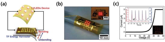
Figure 5. (a) Schematic image of self-powered flexible μLEDs that were composed of flexible red μLEDs and a thin-film piezoelectric power generator. (b) Photograph of flexible red μLED array. The inset image is a top view of the device. (c) I-V curve of flexible μLED arrays. The top inset shows output current and voltage from a thin-film energy harvester. The bottom inset indicates flexible red μLEDs, operated by a piezoelectric energy harvester. Reproduced with permission [32]. Copyright 2014, Royal Society of Chemistry.
Figure 6a displays a monolithic flexible GaN μLED array with a 30 × 30 passive-matrix circuit [31]. Lee et al. developed the monolithic fabrication process for flexible, vertical-structured μLEDs (f-VLEDs). The GaN μLED array was fabricated on a rigid sapphire wafer and then exfoliated with a laser lift-off process. The freestanding GaN μLED array was isolated with epoxy-based polymer. After the electrical interconnection of μLED chips by a silver nanowire (AgNW)-based electrode, the device was passivated by the biocompatible parylene-C layer. After flipping over the device, the AgNW top electrode was made on the device. As shown in the inset images of Figure 6a, the high-density blue μLED array with passive-matrix structure was operated at a bending curvature radius of 5 mm. Since the device was electrically connected by a transparent AgNW network, the μLEDs in off-state were invisible on the human fingernail (Figure 6b and its inset image). According to heat flux simulation, flexible vertical μLEDs had superior thermal stability compared to flexible lateral μLEDs due to efficient heat dissipation through the bottom electrode. The GaN f-VLED displayed excellent mechanical durability during 105 bending/unbending cycles because its mechanical neutral plane was placed at the center of μLED chips (Figure 6c). Furthermore, the device lifetime was expected to last 11.9 years. In accordance with these results, monolithic f-VLEDs are anticipated to commercialize in the display and biomedical device fields.
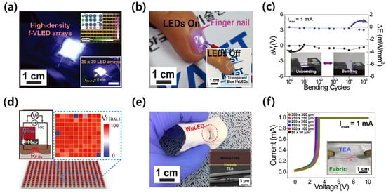
Figure 6. (a) Photograph of monolithic flexible blue μLEDs with 30 × 30 array. The top inset is a magnified optical image of a passive-matrix μLED array. Scale bar: 1 cm. The bottom inset is an optical image of monolithic blue μLEDs in a bent state. (b) Transparent flexible blue μLEDs on human fingernail. The inset image shows fingernail-attached transparent device in off-state. (c) Fatigue test results of monolithic flexible μLEDs during 106 bending/unbending cycles. Reproduced with permission [31]. Copyright 2018, Wiley-VCH. (d) Normalized forward voltage of 50 × 50 μLED arrays with flash-induced Cu electrodes. Reproduced with permission [35]. Copyright 2021, Wiley-VCH. (e) Optical image of wearable red μLED on fabric substrate. The inset is a cross-sectional SEM image of wearable μLED. (f) I-V characteristics of wearable μLEDs with various size. Reproduced with permission [34]. Copyright 2019, Elsevier.
Shin et al. investigated robust Cu electrodes for μLED display applications [35]. Although Cu-based electrodes were spotlighted for application in display circuits due their cheap price, robustness, and high conductivity, Cu had a critical delamination issue on rigid glass substrate. Shin et al. resolved this issue through flashlight-induced Cu-glass interlocking. By radiating a high-powered flashlight on CuO nanoparticles, the CuO was reduced to a conductive Cu layer, simultaneously forming strong adhesion with glass. The 50 × 50 μLED arrays were interconnected with a flash-inducted robust Cu electrode by a thermo-compressive ACF bonding process. The developed device showed thermal/humid stability and high uniformity in large-scale μLED arrays, as shown in Figure 6d. Lee et al. developed wearable μLEDs (WμLEDs) on a 100% cotton fabric [34]. WμLEDs were fabricated using the same protocol with monolithic f-VLED and transferred through transparent elastomeric adhesive by the thermo-compressive process. Figure 6e displays WμLEDs emitting red light at a bent state. The attachment stability between μLED chips and fabric was sophisticatedly investigated by finite element method (FEM) simulation, tensile tests, peel-off tests, digital image correlation (DIC) analysis, and bending fatigue tests. As shown in Figure 6f, WμLEDs with various chip sizes were operated at a forward voltage of ~2.8 V. The WμLEDs showed potential for outdoor application through chemical, thermal, humid, and artificial sunlight tests.
References
- Lee, H.E.; Park, J.H.; Kim, T.J.; Im, D.; Shin, J.H.; Kim, D.H.; Mohammad, B.; Kang, I.-S.; Lee, K.J. Novel Electronics for Flexible and Neuromorphic Computing. Adv. Funct. Mater. 2018, 28, 1801690.
- Joe, D.J.; Kim, S.; Park, J.H.; Park, D.Y.; Lee, H.E.; Im, T.H.; Choi, I.; Ruoff, R.S.; Lee, K.J. Laser-Material Interactions for Flexible Applications. Adv. Mater. 2017, 29, 1606586.
- Kim, S.J.; Lee, H.E.; Choi, H.; Kim, Y.; We, J.H.; Shin, J.S.; Lee, K.J.; Cho, B.J. High-Performance Flexible Thermoelectric Power Generator Using Laser Multiscanning Lift-Off Process. ACS Nano 2016, 10, 10851–10857.
- Lee, H.; Lee, H.E.; Wang, H.S.; Kang, S.; Lee, D.; Kim, Y.H.; Shin, J.H.; Lim, Y.; Lee, K.J.; Bae, B. Hierarchically Surface-Textured Ultrastable Hybrid Film for Large-Scale Triboelectric Nanogenerators. Adv. Funct. Mater. 2020, 30, 2005610.
- Im, T.H.; Lee, C.H.; Kim, J.C.; Kim, S.; Kim, M.; Park, C.M.; Lee, H.E.; Park, J.H.; Jang, M.S.; Lee, D.C.; et al. Metastable quantum dot for photoelectric devices via flash-induced one-step sequential self-formation. Nano Energy 2021, 84, 105889.
- Wang, H.S.; Im, T.H.; Kim, Y.B.; Sung, S.H.; Min, S.; Park, S.H.; Lee, H.E.; Jeong, C.K.; Park, J.H.; Lee, K.J. Flash-welded ultraflat silver nanowire network for flexible organic light-emitting diode and triboelectric tactile sensor. APL Mater. 2021, 9, 061112.
- Lee, H.E.; Shin, J.H.; Lee, S.H.; Lee, J.H.; Park, S.H.; Lee, K.J. Flexible micro light-emitting diodes for wearable applications. In Proceedings of the Light-Emitting Devices, Materials, and Applications, San Francisco, CA, USA, 1 March 2019; Strassburg, M., Kim, J.K., Krames, M.R., Eds.; SPIE: San Francisco, CA, USA, 2019; p. 14.
- Kim, S.J.; Choi, H.; Kim, Y.; We, J.H.; Shin, J.S.; Lee, H.E.; Oh, M.-W.; Lee, K.J.; Cho, B.J. Post ionized defect engineering of the screen-printed Bi 2 Te 2.7 Se 0.3 thick film for high performance flexible thermoelectric generator. Nano Energy 2017, 31, 258–263.
- Kim, D.H.; Lee, H.E.; You, B.K.; Cho, S.B.; Mishra, R.; Kang, I.; Lee, K.J. Flexible Crossbar-Structured Phase Change Memory Array via Mo-Based Interfacial Physical Lift-Off. Adv. Funct. Mater. 2019, 29, 1806338.
- Lee, H.E.; Shin, J.H.; Park, J.H.; Hong, S.K.; Park, S.H.; Lee, S.H.; Lee, J.H.; Kang, I.; Lee, K.J. Micro Light-Emitting Diodes for Display and Flexible Biomedical Applications. Adv. Funct. Mater. 2019, 29, 1808075.
- Park, J.H.; Lee, H.E.; Jeong, C.K.; Kim, D.H.; Hong, S.K.; Park, K.-I.; Lee, K.J. Self-powered flexible electronics beyond thermal limits. Nano Energy 2019, 56, 531–546.
- Jung, D.H.; Park, J.H.; Lee, H.E.; Byun, J.; Im, T.H.; Lee, G.Y.; Seok, J.Y.; Yun, T.; Lee, K.J.; Kim, S.O. Flash-induced ultrafast recrystallization of perovskite for flexible light-emitting diodes. Nano Energy 2019, 61, 236–244.
- Peng, Y.; Que, M.; Lee, H.E.; Bao, R.; Wang, X.; Lu, J.; Yuan, Z.; Li, X.; Tao, J.; Sun, J.; et al. Achieving high-resolution pressure mapping via flexible GaN/ ZnO nanowire LEDs array by piezo-phototronic effect. Nano Energy 2019, 58, 633–640.
- Kim, I.H.; Im, T.H.; Lee, H.E.; Jang, J.; Wang, H.S.; Lee, G.Y.; Kim, I.; Lee, K.J.; Kim, S.O. Janus Graphene Liquid Crystalline Fiber with Tunable Properties Enabled by Ultrafast Flash Reduction. Small 2019, 15, 1901529.
- Park, A.H.; Lee, S.H.; Lee, C.; Kim, J.; Lee, H.E.; Paik, S.-B.; Lee, K.J.; Kim, D. Optogenetic Mapping of Functional Connectivity in Freely Moving Mice via Insertable Wrapping Electrode Array Beneath the Skull. ACS Nano 2016, 10, 2791–2802.
- Lee, H.E.; Kim, S.; Ko, J.; Yeom, H.-I.; Byun, C.-W.; Lee, S.H.; Joe, D.J.; Im, T.-H.; Park, S.-H.K.; Lee, K.J. Skin-Like Oxide Thin-Film Transistors for Transparent Displays. Adv. Funct. Mater. 2016, 26, 6170–6178.
- Lee, H.E.; Park, J.H.; Jang, D.; Shin, J.H.; Im, T.H.; Lee, J.H.; Hong, S.K.; Wang, H.S.; Kwak, M.S.; Peddigari, M.; et al. Optogenetic brain neuromodulation by stray magnetic field via flash-enhanced magneto-mechano-triboelectric nanogenerator. Nano Energy 2020, 75, 104951.
- Jeong, Y.; Lee, H.E.; Shin, A.; Kim, D.; Lee, K.J.; Kim, D. Progress in Brain-Compatible Interfaces with Soft Nanomaterials. Adv. Mater. 2020, 32, 1907522.
- Park, J.H.; Seo, J.; Kim, C.; Joe, D.J.; Lee, H.E.; Im, T.H.; Seok, J.Y.; Jeong, C.K.; Ma, B.S.; Park, H.K.; et al. Flash-Induced Stretchable Cu Conductor via Multiscale-Interfacial Couplings. Adv. Sci. 2018, 5, 1801146.
- Hwang, I.; Kim, H.N.; Seong, M.; Lee, S.-H.; Kang, M.; Yi, H.; Bae, W.G.; Kwak, M.K.; Jeong, H.E. Multifunctional Smart Skin Adhesive Patches for Advanced Health Care. Adv. Healthc. Mater. 2018, 7, 1800275.
- Sreenilayam, S.P.; Ahad, I.U.; Nicolosi, V.; Acinas Garzon, V.; Brabazon, D. Advanced materials of printed wearables for physiological parameter monitoring. Mater. Today 2020, 32, 147–177.
- Jin, H.; Abu-Raya, Y.S.; Haick, H. Advanced Materials for Health Monitoring with Skin-Based Wearable Devices. Adv. Healthc. Mater. 2017, 6, 1700024.
- Lo, L.; Shi, H.; Wan, H.; Xu, Z.; Tan, X.; Wang, C. Inkjet-Printed Soft Resistive Pressure Sensor Patch for Wearable Electronics Applications. Adv. Mater. Technol. 2020, 5, 1900717.
- Yang, J.C.; Mun, J.; Kwon, S.Y.; Park, S.; Bao, Z.; Park, S. Electronic Skin: Recent Progress and Future Prospects for Skin-Attachable Devices for Health Monitoring, Robotics, and Prosthetics. Adv. Mater. 2019, 31, 1904765.
- Yeon, H.; Lee, H.; Kim, Y.; Lee, D.; Lee, Y.; Lee, J.S.; Shin, J.; Choi, C.; Kang, J.H.; Suh, J.M.; et al. Long-term reliable physical health monitoring by sweat pore–inspired perforated electronic skins. Sci. Adv. 2021, 7, 1–11.
- Xi, D.; Xiao, M.; Cao, J.; Zhao, L.; Xu, N.; Long, S.; Fan, J.; Shao, K.; Sun, W.; Yan, X.; et al. NIR Light-Driving Barrier-Free Group Rotation in Nanoparticles with an 88.3% Photothermal Conversion Efficiency for Photothermal Therapy. Adv. Mater. 2020, 32, 1907855.
- Xu, X.; Chen, J.; Cai, S.; Long, Z.; Zhang, Y.; Su, L.; He, S.; Tang, C.; Liu, P.; Peng, H.; et al. A Real-Time Wearable UV-Radiation Monitor based on a High-Performance p-CuZnS/n-TiO2 Photodetector. Adv. Mater. 2018, 30, 1803165.
- Wang, C.; Xia, K.; Zhang, Y.; Kaplan, D.L. Silk-Based Advanced Materials for Soft Electronics. Acc. Chem. Res. 2019, 52, 2916–2927.
- Zodrow, K.R.; Li, Q.; Buono, R.M.; Chen, W.; Daigger, G.; Dueñas-Osorio, L.; Elimelech, M.; Huang, X.; Jiang, G.; Kim, J.-H.; et al. Advanced Materials, Technologies, and Complex Systems Analyses: Emerging Opportunities to Enhance Urban Water Security. Environ. Sci. Technol. 2017, 51, 10274–10281.
- Cai, S.; Xu, X.; Yang, W.; Chen, J.; Fang, X. Materials and Designs for Wearable Photodetectors. Adv. Mater. 2019, 31, 1808138.
- Lee, H.E.; Choi, J.H.; Lee, S.H.; Jeong, M.; Shin, J.H.; Joe, D.J.; Kim, D.H.; Kim, C.W.; Park, J.H.; Lee, J.H.; et al. Monolithic Flexible Vertical GaN Light-Emitting Diodes for a Transparent Wireless Brain Optical Stimulator. Adv. Mater. 2018, 30, 1–10.
- Jeong, C.K.; Park, K.-I.; Son, J.H.; Hwang, G.-T.; Lee, S.H.; Park, D.Y.; Lee, H.E.; Lee, H.K.; Byun, M.; Lee, K.J. Self-powered fully-flexible light-emitting system enabled by flexible energy harvester. Energy Environ. Sci. 2014, 7, 4035–4043.
- Lee, H.E.; Lee, S.H.; Jeong, M.; Shin, J.H.; Ahn, Y.; Kim, D.; Oh, S.H.; Yun, S.H.; Lee, K.J. Trichogenic Photostimulation Using Monolithic Flexible Vertical AlGaInP Light-Emitting Diodes. ACS Nano 2018, 12, 9587–9595.
- Lee, H.E.; Lee, D.; Lee, T.; Ho, J.; Choi, G. Wireless Powered Wearable Micro Light-Emitting Diodes. Nano Energy 2018, in press.
- Shin, J.H.; Park, J.H.; Seo, J.; Im, T.H.; Kim, J.C.; Lee, H.E.; Kim, D.H.; Woo, K.Y.; Jeong, H.Y.; Cho, Y.; et al. A Flash-Induced Robust Cu Electrode on Glass Substrates and Its Application for Thin-Film μLEDs. Adv. Mater. 2021, 33, 2007186.
- Woodgate, G.J.; Harrold, J. P-101: Micro-Optical Systems for Micro-LED Displays. SID Symp. Dig. Tech. Pap. 2018, 49, 1559–1562.
- Marinov, V.R.; Swenson, O.; Atanasov, Y.; Schneck, N. Laser-assisted ultrathin die packaging: Insights from a process study. Microelectron. Eng. 2013, 101, 23–30.
- Kim, R.-H.; Bae, M.; Kim, D.G.; Cheng, H.; Kim, B.H.; Kim, D.-H.; Li, M.; Wu, J.; Du, F.; Kim, H.-S.; et al. Stretchable, Transparent Graphene Interconnects for Arrays of Microscale Inorganic Light Emitting Diodes on Rubber Substrates. Nano Lett. 2011, 11, 3881–3886.
- Kim, T.; Jung, Y.H.; Song, J.; Kim, D.; Li, Y.; Kim, H.; Song, I.-S.; Wierer, J.J.; Pao, H.A.; Huang, Y.; et al. High-Efficiency, Microscale GaN Light-Emitting Diodes and Their Thermal Properties on Unusual Substrates. Small 2012, 8, 1643–1649.
- Lee, S.H.; Kim, J.; Shin, J.H.; Lee, H.E.; Kang, I.-S.; Gwak, K.; Kim, D.-S.; Kim, D.; Lee, K.J. Optogenetic control of body movements via flexible vertical light-emitting diodes on brain surface. Nano Energy 2018, 44, 447–455.
More
Information
Subjects:
Engineering, Biomedical
Contributor
MDPI registered users' name will be linked to their SciProfiles pages. To register with us, please refer to https://encyclopedia.pub/register
:
View Times:
884
Revisions:
2 times
(View History)
Update Date:
05 Nov 2021
Table of Contents


Notice
You are not a member of the advisory board for this topic. If you want to update advisory board member profile, please contact office@encyclopedia.pub.
OK
Confirm
Only members of the Encyclopedia advisory board for this topic are allowed to note entries. Would you like to become an advisory board member of the Encyclopedia?
Yes
No
${ textCharacter }/${ maxCharacter }
Submit
Cancel
Back
Comments
${ item }
|
${ item.createdUser.fullName }
${ item.createdAt }
${ item.vote }
${ item.reply }
Delete
${ reply.createdUser.fullName }
${ reply.createdAt }
${ reply.vote }
Delete
There is no reply to this comment~
${ item.replyTextCharacter }/${ item.replyMaxCharacter }
Submit
Cancel
More
No more~
There is no comment~
${ textCharacter }/${ maxCharacter }
Submit
Cancel
${ selectedItem.replyTextCharacter }/${ selectedItem.replyMaxCharacter }
Submit
Cancel
Confirm
Are you sure to Delete?
Yes
No