 +1 credit
| Version | Summary | Created by | Modification | Content Size | Created at | Operation |
|---|---|---|---|---|---|---|
| 1 | Salvatore Musumeci | + 10050 word(s) | 10050 | 2021-10-11 04:38:48 | | | |
| 2 | Bruce Ren | -2 word(s) | 10048 | 2021-10-29 03:37:49 | | |
Video Upload Options
The efficiency and power density improvement of power switching converters play a crucial role in energy conversion. In the field of motor control, this requires an increase in the converter switching frequency together with a reduction in the switching legs’ dead time. This target turns out to be complex when using pure silicon switch technologies. Gallium Nitride (GaN) devices have appeared in the switching device arena in recent years and feature much more favorable static and dynamic characteristics compared to pure silicon devices. In the field of motion control, there is a growing use of GaN devices, especially in low voltage applications.
1. Introduction
In the application scenario of motion control, low voltage high dynamic drives are widely used. The low voltage drives (<100V) are applied in several advanced technological fields such as robotics, home appliances, warehousing automation, CNC machines, e-mobility and unmanned aerial vehicles (UAVs), etc [1][2][3]. The electrical drive's dynamic performances are strongly influenced by the technology of the power switches on which the inverter's topology is based. In the field of low voltage switching devices (with breakdown voltage up to 100V), the silicon (Si) MOSFETs in trench-gate technology are the low-cost standard switches available in a wide range of current ratings and can reach quite satisfactory high switching frequencies [4][5]. Nowadays, high electron mobility transistors (HEMT) Gallium Nitride (GaN) devices are becoming increasingly used, especially in low voltage applications due to their superior features such as high dynamic characteristics, high power density, very high-temperature ratings, compared to pure silicon MOSFET devices, with similar current rating [6]. In high voltage applications, the GaN devices are in continuous development and compete with Silicon Carbide (SiC) MOSFETs, Silicon (Si) super junction MOSFETs, and IGBTs, which have a higher technological maturity [7]. The penetration of GaN devices in these sectors is still partial due to the lower breakdown voltage (until 650V, currently available in the market) and only for specific applications with high switching frequency (up to a few MHz range) [7].
In low voltage applications for power ratings up to 400W, there are also integrated switching leg solutions which include the driver circuit in the same package. This monolithic approach acts by reducing parasitic inductances and optimizing the switching performance to reduce losses and ringing voltage, thus allowing the designer to downsize the cooling requirements and improve the converter reliability [8]. For a higher power rate, discrete GaN FETs (Field Effect Transistors) are used to reach high current density switching legs. However, the wide bandgap (WBG) GaN devices allow higher switching frequency in inverter topologies for drives applications compared with silicon MOSFETs. The switching frequency increase also leads to some advantages. It minimizes the current ripple in the motor and enables the reduction of the overall capacitance value in the DC link allowing the replacement of electrolytic with smaller non-polarized capacitors [9]. Furthermore, the GaN FETs high switching transients both in the rise time and the fall time leads to a strong reduction of the dead time in the switching leg circuits. In the inverter leg, a dead time duration influences the quality of the output waveforms of the voltage increasing the number of harmonics, thus worsening the total harmonic distortion (THD) [10]. The waveforms distortion caused by dead time is affected by its length, given the switching frequency and the input DC voltage. The reduction of the dead time enabled by the advanced GaN FETs as switches solution improves the shape of the waveforms without the use of dedicated software resources to compensate for the waveforms distortion drawbacks [11].
In this paper, the main advantages and disadvantages of GaN FETs in inverter topologies for low voltage high dynamic performance electrical drives are analyzed and discussed. The impact of the HEMT devices in high power density electrical drives evolution is pointed out considering the state of art and perspectives. The use of GaN FETs allows integration of the inverter topologies with AC motors to realize a compact and reliable motor control system [12], [13]. The integration of the electric machine and its driving topology lead a benefit of the electric motor drive modularity avoiding electrical cables reducing the voltage ringing and EMI contents [14]. Furthermore, in an integrated modular motor drive (IMMD) the cooling system can be achieved by the motor case. These benefits are more noticeable in multiphase motor drives [15].
The article provides a wide investigation on the extensive use of low voltage GaN FETs devices in motion control applications. Clear information to the designers on the technological and application benefits of these HEMT devices for ever smaller and more reliable applications of electric drives is carried out. The troublesome features of these devices are also considered to provide possible solutions or reductions in drawbacks. The GaN FETs advantages and issues primarily are carried out by an experimental investigation approach. The main results are obtained using two experimental inverter boards. In one of these experimental boards, the switching legs are implemented with an integrated solution, while the other inverter board is equipped with higher power density GaN FETs to evaluate several operative conditions.
Furthermore, the paper deals with the impact of the switching frequency increasing of GaN FETs in the design of inverter DC link capacitors. In addition, the problems of high dv/dt and the benefits of dead time reduction are explored. Moreover, the problems of layout and reductions of parasitic inductances are pointed out. The current measurement conditions in the noise environment due to the highest achievable switching frequencies are considered too.
The paper is structured as in the following: in section 2 the power stages are described considering the technology issue the layout matter and the main gate driver requirements. In section 3, the input current and voltage ripple issues are analyzed at increasing switching frequency to evaluate the impact on the passive device design. In section 4 the dead time reduction benefits are considered and discussed. In section 5, the voltage transients (dv/dt) effect in switching leg and in motor drive application is further investigated. Finally, in section 6, a switching evaluation of an enhanced inverter board with a discrete GaN FETs solution is carried out.
2. GaN FETs-Based Inverter Legs Power Stage
2.1. Low-Voltage GaN FETs Operation and Technology Survey
-
gate threshold,
-
conduct resistance and temperature behavior,
-
structure parasitic capacitors,
-
reverse conduction mode.

Considering the thermal behavior, the GaN FET shows a positive temperature coefficient such as the MOSFET device [18].

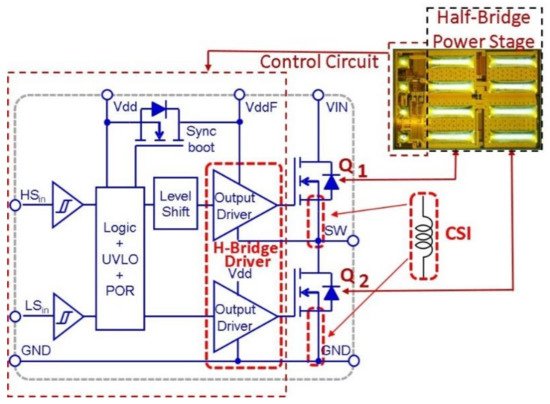
2.2. Packaging Issue and Integrating Solutions
2.2.1. Power Stage Integration

2.3. Inverter Circuit Arrangement
2.3.1. Notes on the Inverter Legs Layout
2.3.2. Driver Circuit Requirements
2.3.3. Current Sensing Arrangement
3. Input Current and Voltage Ripple Issues
The DC-link capacitor balance fluctuates instantaneous power exchange between the battery and the inverter. The DC-Link capacitor stabilizes the “ripple” caused by the inverter high-frequency power switching circuits. In the system performance, a reliable and small-size DC-link capacitor plays a key role. Typically, four types of capacitors such as Aluminium Electrolytic capacitor, Metalized Polypropylene Film Capacitor, Tantalum polymer, and hybrid polymer, and Multilayer Ceramic capacitor are available as a DC-link capacitor. Headline capacitor specifications are related to size, cost, lifetime, and reliability matter. Other parameters to control are Capacitance/Voltage (CV) ratio, Equivalent Series Resistance (ESR), low stray inductances, ripple current rating, and working temperature. The best capacitor selection depends on a trade-off among these parameters. It is strongly connected to the capacitance values needed by the capacitor link to reduce both the input voltage and current ripple. The switching frequency increase pursuits the capacitor values reduction.
The typical MOSFET-based inverters for battery-operated motor drive applications run at a PWM frequency in the range of 20-40 kHz. In battery-operated inverters running at 20 kHz PWM, there is a critical voltage and current ripple across the inverter's battery cables. Usually, the voltage ripple is a square wave, and the current ripple is a triangular wave. These ripples on the battery cable are a source of EMC (radiated and conducted) and stress the battery, reducing its lifetime. The typical industrial solution is to reduce this stress using a DC-side LC filter. This LC input filter reduces both ripples at the expense of the system's efficiency, volume, weight, reliability, and lifetime.
In a battery-powered inverter, the input current iD(t) is the sum of three components: the DC average current (ID), the low-frequency, and the high-frequency (at the switching frequency) component (delta iD). In the case of a balanced load, such as a BLDC motor, the low-frequency component is zero. Therefore, the input instantaneous current is

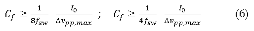
The design of the capacitor (Cf) value is based on the expected voltage ripple. The peak-to-peak DC-Link voltage ripple amplitude Dvpp is related to the high-frequency current component.

Where ts is the specific application time interval fixed by the space vector modulation strategy. From (5) the capacitance value of Cf can be calculated. This design approach takes into account the behavior of the current and voltage ripple shapes in the case of symmetrical space vector modulation. This capacitor value design procedure is based on reference [29]. In this analytical methodology, two operating conditions are considered. In the first case, a purely resistive load is supposed (angle = 0). In the second case, the worst operative condition is presumed, with a purely inductive load (angle= 90°). The two relations to achieve the correct input capacitor value in the two considered conditions are
As it can be seen from the two relations recalled in (6), as the frequency increases, the capacitance value decreases for a given peak-to-peak ripple voltage [29]. The inductance of the input LC filter (Figure 10a) can be calculated from the LC resonant frequency
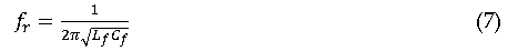
The fr is typically chosen at 1/10 of the switching frequency to obtain a proper filtering action of the PWM components. The value of the filter values versus switching frequency fsw is depicted in Figure 10b, considering capacitor Cf extracted in the worst case of (6) and Lf by means of (7) with fr=1/10 fsw, considering a theoretical delta vpp=1V. From the results shown in Figure 10b the strong reduction of the passive filter components at increasing switching frequency is evident.
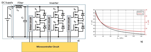
Figure 10. (a) Simplified low pass filter schematic in the input side of the battery-powered inverter, (b) Graphic of the passive component of the filter versus the switching frequency.
3.1. Experimental Evaluation of the Input Electrical Quantities Versus Switching Frequency Variation
The objective of this experimental investigation is to correlate the filter components and the input electrical quantities behavior versus the switching frequency variation. The low pass filter components in the experimental board are from a standard 20kHz MOSFET inverter for 250W BLDC motor drive with monolithic switching leg (e-bike application). The LC filter values are Lf=2.7µH, the electrolytic capacitor Cf=660μF obtaining about 200mV of delta vpp. The output current I0 is fixed at 5A rms and the input voltage is 36V.
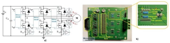
In the preliminary experimental results presented, the filter capacitor size improving versus switching frequency increasing is focused. Two operative conditions are highlighted. The first one is at 20kHz with an electrolytic capacitor in the filter cell. In the second case, a modulation strategy with a switching frequency of 100kHz is implemented. In this last case, three kinds of capacitors (Aluminium electrolytic, tantalum, and ceramic capacitors) are involved in the switching evaluation to obtain a voltage ripple peak equivalent at the basic case at 20kHz. In Figure 11a the experimental setup picture is shown. In Figure 11b the zoomed of the electrolytic capacitors filter cell is reported. In Figure 11c the ceramic capacitors filter cell is depicted. Finally, the Tantalum solution is shown.
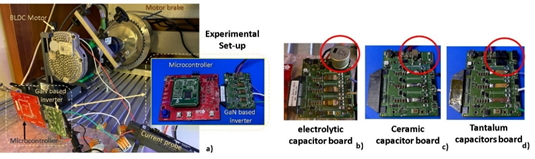
Figure 11. (a) Picture of the experimental Setup with a zoomed view of microcontroller and GaN FET based inverter (b) Inverter board with electrolytic capacitor filter. c) Inverter board with ceramic capacitor filter. d) Inverter board with tantalum capacitor filter.
In Figure 12a and Fig. 12b, the switching waveforms at 20kHz and 100kHz with the designed filter with electrolytic capacitors (2 electrolytic capacitors with a value of 330uF) are shown. The Aluminium electrolytic capacitor with increasing switching frequency shows its limits. As arise comparing the Figure 12a and Figure 12b the current ripple at 100kHz is reduced but the electrolytic capacitor due to the parasitic components features a ringing noise on a voltage ripple making useless the improvement obtained on the current ripple.
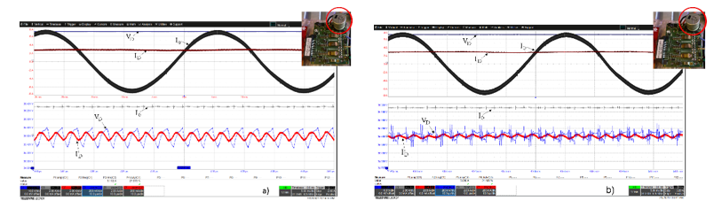
Figure 12. Switching waveform with Cf=660mF dead time 21ns at I0 =Ia=5A rms VDC=36V, (a) 20kHz of the switching frequency, (b) 100kHz of the switching frequency. Upper waveforms VD=10V/div, ID=2A/div, I0=2A/div, t=5ms bottom zoomed waveforms VD=200mV/div, ID=200mA, I0=2A/div, a) t=50ms, b) t=10us.
At 100 kHz maintaining the same peak-to-peak level of the ripple voltage, a lower value capacitor can be used. From design considerations that will be addressed in the full paper based on the description of the previous section, the same ripple level is obtained by a capacitor approximately equal between 22 and 30 μF. These lower capacitance values can be obtained with other more performing high frequencies capacitor technologies in both polarized and non-polarized solutions. In Figure 13a the Cf is equal to 22μF in ceramic technology. In Figure 13b the same voltage ripple level is obtained by means of 30mF Tantalum capacitors. Ceramic capacitors are more attractive because they are used in DC to RF frequency. They are capable of handling high voltages. Furthermore, they feature low ESR and equivalent series inductance (ESL) with the volume quite reduced. Tantalum capacitors are high density of capacitance thus smaller package sizes are obtainable with respect ad aluminum electrolytic capacitors. They have lower leakage currents and stability characteristics with higher costs.
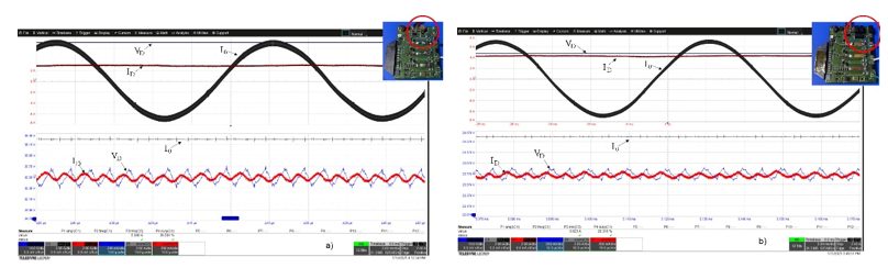
Figure 13. Switching waveform with a dead time of 21ns at I0=Ia=5A rms VD=36V, 100kHz of the switching frequency (a) Cf ceramic equal to 22μF, (b) Cf tantalum equal to 30μF. Upper waveforms VD=10V/div, ID=2A/div, I0=2A/div, t=5ms bottom zoomed waveforms VD=200mV/div, ID=200mA, I0=2A/div, t=10us.
4. Dead Time Effect on the Motor Drives Inverters
In voltage source inverters, the dead time is necessary to avoid the bridge shoot-through during switching operation. However, the dead time should be chosen as small as possible to limit the equivalent voltage drop at the inverter output. Moreover, GaN devices operate in reverse conduction mode during the dead time. In fact, in GaN FETs no body diode reverse recovery is present. Instead, the voltage of the GaN devices is larger than the usual of body diodes in Si MOSFETs. Therefore, the dead time must be chosen accurately to the smallest possible value to reduce the power losses. In general, the dead time tdt,off must cover the switching time of the GaN device. Considering the lower device turn-off dead time tdt,off must be higher than the off transient delay time td,off and the transient time tsw,off.

A similar dead time evaluation for the Q2 turn-on (tdt,on) switching event may be considered. In the dead time duration, the body diode equivalent free-wheeling acts introducing further power losses described in (15). Where the voltage drop VF depends on the GaN FET technology characteristics.

The on-dead time on tdt,on, and the off-dead time off tdt,off can be chosen also in different ways based on the application request [30]. If tdt,on is equal to tdt,off the dead time is simply defined as tdt. From the modeling of the dead time starting from (9), it is possible to evaluate the losses related to the variation of the dead time at different output currents as shown in Figure 14a. As shown in Figure 14a, dead-time losses due to body diode voltage drop VF increase linearly versus the total dead-time widening. Dead-time losses due to Qrr are absent. While in the MOSFETs the Qrr losses are noticeable [31]. The comparative qualitative waveforms of the power losses for MOSFETs and GaN FETs are reported in Figure 14b [32]. Despite the lower losses due to the reduced voltage VF in the MOSFETs, the contribution of body diode Qrr produces greater losses as the dead time decreases.
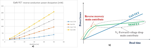
Figure 14. (a) Dead time power losses versus a dead time variation at different output currents (EPC2206 GaN FET). (b) Qualitative curves for comparison of dead time losses for MOSFETs and GaN FETs.
In the inverter leg, the dead time influences the quality of the output waveforms of the voltage increasing the number of harmonics, thus worsening the total harmonic distortion (THD) [10]. The distortion created by dead time is affected by its length, given the switching frequency and the input DC voltage. The reduction of both the rise time and the fall time with GaN FET used as switches leads to a strong reduction of the dead time in the leg switching circuits.
In the inverter leg shown in Figure 15a, the gate commands are obtained by comparing the triangular carrier signal with the modulation control voltage, as reported in Figure 15b. The dead time is necessary to avoid the cross conduction of the switching devices, but it introduces a non-linear effect that influences the output waveforms quality [11][33]. This leads to an output phase voltage error, which can be expressed as follows [33][33]:
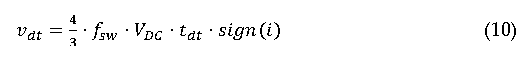
and depends on the sign of the inverter phase current. The voltage average output waveforms are affected by a discontinuity when the current changes its sign, as shown in Figure 15c.
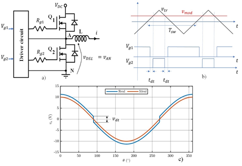
Figure 15. (a) simplified inverter switching leg schematic, (b) Phase A, control signal generation by PWM technique with dead time. (c) Dead time effect on the moving average value of the inverter output voltage.
The output average voltage related to phase A is related to the dead time width and the current sign. The voltage average output waveforms are affected by a discontinuity when the current changes its sign, as shown in Figure 15c. The output average voltage related to phase A is related to the dead time width and the current sign.
The effect of this voltage distortion can be visualized more easily if represented in the (α,β) frame and in the (d,q) rotating frame [34], synchronous with the phase current i. The result of this transformation is depicted in Figure 16. It is evident that the dead time distortion leads to an almost constant voltage error in the direct axis (i.e., voltage error at the fundamental frequency) and a zero-mean value error at six times the fundamental frequency on the quadrature axis [10],[34]. This means that there will be a distortion in the fundamental component of the current and one at higher harmonic order. While the first one can be easily compensated by the current regulator integral part, the latter is the source of non-compensated distortions, which influence the phase current, as they might be above the bandwidth of the current loop. Another effect of the dead time is well-known in the field of sensorless control. In such applications, the control techniques use observers and estimators to orient the control frame to the actual one of the electrical machine. These algorithms require the reconstruction of the voltage applied to the inverter, and must, therefore, consider also its non-ideal behavior to avoid introducing orientation errors [33][35].
The non-linearity on the average voltage output waveforms related to the above-mentioned dead time distortions is usually compensated by implementing various open-loop and closed-loop algorithms [11], [36][37][38], which also include self-commissioning techniques to identify the magnitude of these voltage drops [35].
In this paper, a simple and straightforward open-loop compensation algorithm has been considered. This method simply adds a feed-forward term, opposite to the dead time voltage drop when the phase current changes its polarity. The quality of this software solution depends on the correct sensing of the current sign. Other more sophisticated techniques may improve the compensation performance. However, they often require much more complex algorithms or hardware modifications, which would burden the control system and increase its complexity and tuning.
To avoid any compensation and largely improve the quality of the current waveform, the best option is to reduce the dead time duration.
In the case of GaN FET application as switches in inverter leg, the dead time can be selected in the range of tens of ns, therefore making the hardware solution very attractive compared to the software technique because it implies a saving of software and hardware resources.
4.1. Simulation and Experimental Results
The evaluation of the dead time selection is carried out by implementing a three-phase inverter driving a BLDC in a software tool (PLECS©). The inverter dc bus is fixed to 48 V, the maximum motor load current is equal to 10 A, the switching frequency is set to 40 kHz, and the control frequency to 20 kHz. In the first simulation results, a dead time of 500 ns (typical of the Si MOSFET) is compared with a dead time of 14 ns, easily available with the latest generation of the GaN FETs.
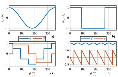
Figure 16. Dead time effect modeling in the stationary reference frame and in the synchronous reference frame. a)Top left: current of the phase a. b)Top right: c)Bottom left: function in per unit in the stationary (α,β) frame. d) Bottom right: function in per unit in the rotating (d,q) frame, synchronous with the phase a current.
In the first simulation result, a dead time equal to 14 ns leads to a negligible speed ripple compared to the case of dead time equal to 500 ns (Figure 17a). In the second simulation result, the speed ripple of the dead time selected at 14 ns is compared with the dead time compensation technique in the case of the dead time equal to 500 ns. As shown in Figure 17b the peak-to-peak amplitude of the speed ripple is more symmetric in the case of 14ns dead time. Furthermore, the maximum peak values are similar.
Figure 17. Dead time effect in the speed ripple. (a) Dead time equal to 500 ns compared with the case of dead time of 500ns with compensation and dead time reduced of 14ns. (b) Magnified view of Figure 17a for the speed ripple comparison at 14ns of dead time and 500ns dead time with software compensation.
The current waveforms in the case of 14 ns dead time show a very low waveform distortion compared to the 500 ns dead time with and without software compensation. In Figure 18a the simulation of the phase a current is reported at 500ns (i500ns) of dead time compared with the case of 500ns with compensation (i500ns,C) and the case of the dead time equal to 14ns (i14ns). The zoomed view of the current across the passage for 0 in the three cases is shown in Figure 18b. The better waveform shape with 14ns arises from the inspection view of Figure 18b.
As consequence considering the comparison of the load current harmonic spectrum, the lowest harmonic content is obtained in the case with a dead time of 14 ns as in Figure 18c.
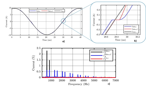
Figure 18. (a) Dead time effect on the current waveform of phase a in the three cases considered. (b) zoomed view of current zero-crossing in the three cases of study. (c) Harmonic content comparison for the load current in the case of dead time equal to 14 ns, 500 ns, and 500 ns with compensation.
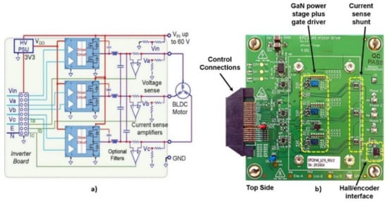
The experimental results were carried out on an EPC9146 [17] board, driving a BLDC motor, as it can be seen in the block diagram of Figure 19a. The tested motor drive was operating from a 48 V dc supply voltage delivering up to 3.7 Arms into each phase of the motor with a Field Oriented Control (FOC) [39]. We used a 40 kHz PWM frequency (20 kHz control frequency) and 500 ns dead time that is typical of Si MOSFET-based inverters. The view of the experimental set-up is reported in the picture of Figure 19b.
Three tests were carried out at a mechanical speed :
- ns with no dead time compensation algorithm (see Figure 20);
- ns with the compensation algorithm described previously (see Figure 21);
- ns with no dead time compensation algorithm (see Figure 22).
As it can be seen in these waveforms, the 500 ns dead time is significantly distorting the phase current. This can be highlighted from a spectral analysis of both the phase current and mechanical torque. As it is displayed in Figure 20, the dead time distortions lead to a large harmonic content at the 5th and 7th harmonic on the phase current, corresponding to the 6th harmonic in the mechanical torque [40].
This effect can be mitigated by implementing a dead time compensation strategy, leading to the results of Figure 21. As it can be clearly seen in the current and torque spectrum, the compensation strategy greatly improves the quality of the electrical and mechanical quantities, reducing the low order harmonic content. These harmonics are, however, not fully compensated, since the adopted method is based on an open-loop paradigm [40].
Adjusting the dead time to 14 ns, which is something that can only be achieved with GaN devices, the waveforms greatly improve, as it emerges from the results of Figure 22. The phase current waveform is much smoother with a 14 ns dead time and the effect is clearly highlighted by the spectral analysis, where the low order harmonics are almost eliminated.
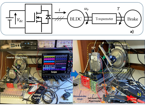
Figure 19. (a) Diagram of the experimental setup. The BLDC drive is connected to a brake to regulate the torque loading, (b) Photo of the experimental setup.
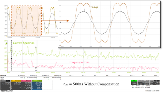
Figure 20. Motor current in the time domain and DFT of phase current and machine mechanical torque 50 ms/div. and no compensation algorithm. C5: motor phase current =5A/div. F1: reconstructed inverter voltage =5 V/div. F2: DFT of the mechanical torque 500 mV/Nm. F4: DFT of the inverter phase current.
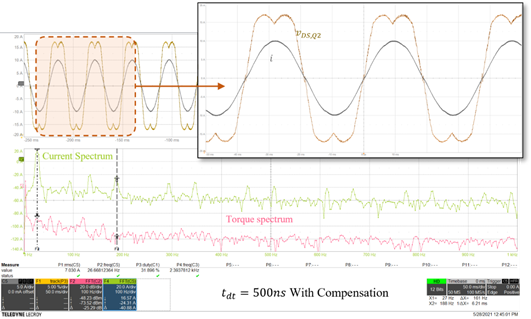
Figure 21. Motor current in the time domain and DFT of phase current and machine mechanical torque 50 ms/div. and no compensation algorithm. C5: motor phase current =5A/div. F1: reconstructed inverter voltage =5 V/div. F2: DFT of the mechanical torque 500 mV/Nm. F4: DFT of the inverter phase current.
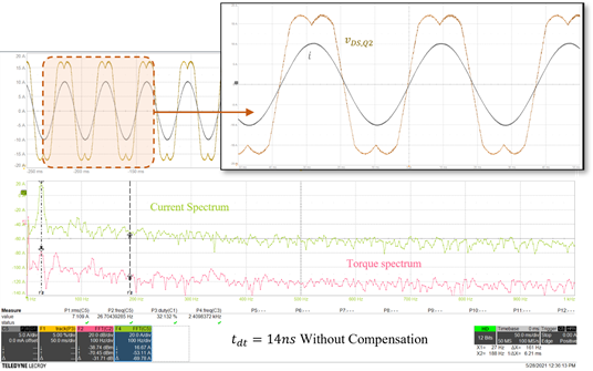
Figure 22. Motor current in the time domain and DFT of phase current and machine mechanical torque 50 ms/div. with no compensation algorithm. C5: motor phase current =5A/div. F1: reconstructed inverter voltage =5 V/div. F2: DFT of the mechanical torque 500 mV/Nm. F4: DFT of the inverter phase current.
5. dv/dt Effect in Switching Leg
In GaN FET device the high dv/dt achievable leads to some consideration in inverter applications. The sinusoidal control voltage of the inverter causes a dv/dt variation during a commutation cycle. in Figure 23a and Figure 23b, the phase node voltage rising and falling edges switching are reported. The switching waveforms are carried out at a peak phase current Ipeak=15 A and Vdc=48V at 50kHz of switching frequency. The experimental waveforms of Figure 23 are obtained with infinite persistence to show the dv/dt range of variation. The time limits of the dv/dt waveforms set the minimum dead time tdt duration (tdt,on=tdt,off=50ns in the discrete GaN FETs based inverter for the experimental validation).
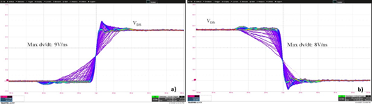
Figure 23. Experimental waveforms were obtained with infinite persistence to show the dv/dt range of variation. (a) Rising edge switching of the node voltage VDS relative to the phase a. (b) Falling edge switching of the node voltage VDS relative to the phase a. VDS,LS=10V/div, t=10ns/div.
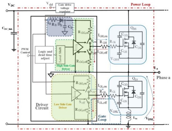
In GaN FETs the threshold voltage, VGSTH is lower than equivalent current density MOSFET devices. In the GaN switch used in the inverter experimental board, the VGSTH is in the range of 1.5 to 2.5 V. This low threshold voltage could cause spurious turn on when the device in off-state is under high dv/dt events. In high dv/dt applications the gate driver constraints are crucial to avoid the shoot-through phenomena. The switching leg circuit with the gate driver interaction and the high dv/dt current paths are shown in Figure 24a
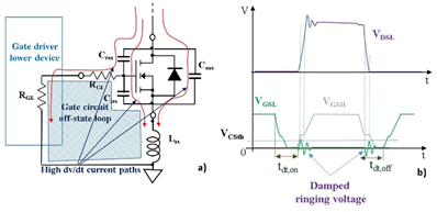
Figure 24. (a) Low side GaN FET device in off-state current paths and parasitic passive components model. (b) qualitative switching waveforms of the node voltage, low-side gate voltage VGSL, and high-side gate voltage VGSH.
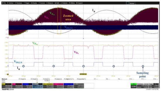
While the qualitative waveforms of the node voltage switching and the gate voltage of the higher and lower devices are reported in Figure 24b. The gate voltage requirements can be achieved by reducing critical damping of the gate drive turn-on switching due to the interaction with the power loop by means of accurate layout design. In addition, the turn-on and turn-off transient’s requirements are different which necessitates the use of independent gate resistors to adapt the turn-on and turn-off gate-loop damping. Considering the low side device, the parasitic source inductance produces an oscillation on the gate voltage at the dv/dt of the node voltage of the switching leg. The ringing voltage is dependent on the switching frequency. At switching frequencies up to 100kHz, the contribution of inductance is reduced compared to the cases of DC-DC converters operating at MHz frequencies. Therefore, in correspondence with dv/dt, the peak due to the parasitic input capacities will mainly be detected as shown in Figure 25.
The experimental waveforms depicted in Figure 25 are carried out at turn-on of the higher switch of an inverter leg with the lower device in off condition at 10A of phase current. From the observation of Figure 25 is possible to note the reduced gate voltage spike in the lower leg device (zoomed view with tzoom=50ns) in correspondence with the high dv/dt of the node voltage. This spurious pulse is under the VGSTH thanks to the mixed effect of the reduced parasitic capacitance of GaN FET and a suitable driver circuit solution.
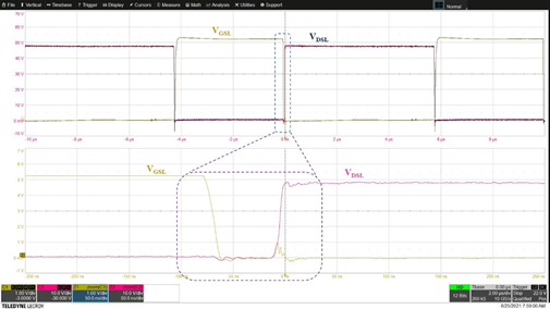
Figure 25. Experimental waveforms of the gate-source voltage of the lower device of inverter leg (phase a) under the rise of the of the inverter leg node voltage (lower device - drain-source voltage). The dv/dt effect acts a gate voltage spike under the GaN threshold voltage (VGSTH) VDSL=10V/div, VGSL=1V/div, tmain=2ms, tzoom=50ns/div.
6. Discrete GaN FET Based Inverter Switching Evaluation
In this section, a Permanent Magnet AC (PMAC) PMAC motor is driven by the GaN FETs based inverter with a sensor-less FOC technique implemented in a microcontroller circuit [41]. The load current variation is obtained by a suitable motor brake. The main characteristics of the motor used are reported in Table 1. In Table 2 the test conditions of the inverter board are recalled. The experimental evaluation is carried out without heat-sink in inverter operation. In Figure 26a the input and output waveforms for two phases at switching frequency fsw=50kHz and Ia,b,rms=15A are reported.
In Figure 26b the input and output experimental waveforms in the operative conditions of Ia,b,rms=10A at 100kHz are carried out. From an inspection of the switching waveforms of Figure 26b, the advantage is that the input voltage and current ripple decrease when the PWM frequency is increased, allowing the designer to remove the electrolytic capacitors and use only ceramic that are smaller, lighter, and more reliable as better described in section 3. The experimental board is composed on the top surface with ceramic capacitors and on the bottom with electrolytic capacitors that can be removed when the switching frequency increase. The current waveform of phase a, with the first harmonic of the phase voltage, is depicted in Figure 27a, while in Figure 27b the zoomed view of the current ripple and the voltage pulses at 100kHz of switching frequency for the same inverter phase are reported.
Finally, the inverter efficiency in the three cases reported in Table 2 is described in Figure 28. The efficiency is quite similar in the range of 20-50kHz. At 100kHz the efficiency is quite high but slightly lower than the previous cases.
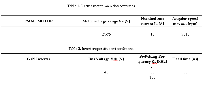
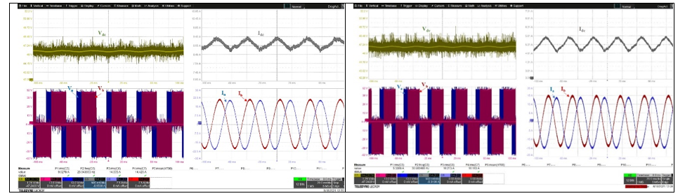
Figure 25. (a) Experimental waveforms of the input and output inverter quantities at fsw=50kHz. Vdc= 1.24V/div, Idc=500mA/div, Va=Vb=13V/div, Ia=Ib=7.5A/div, t=20ms/div. (b) Experimental waveforms of the input and output inverter quantities at fsw=100kHz. Vdc= 1.24V/div, Idc=500mA/div, Va=Vb=13V/div, Ia=Ib=5A/div, t=20ms/div.
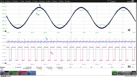
Figure 26. Experimental waveforms of output voltage and current of phase a. a) phase current and first harmonic of output inverter voltage. Ia=5A/div, Va1=5V/div, tmain=10ms. b) Voltage pulses and current ripple. a) 1.24V/div, Ia=500mA/div, Va=13V/div, tzoom=20ms/div.
Figure 27. Inverter efficiency at motor current variation (rms) for three switching frequencies: 20kHz, 50kHz, 100kHz.
6.1. Thermal Behavior
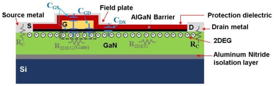
Gallium nitride-based HEMT devices feature, like silicon power MOSFETs, a positive coefficient temperature suitable for the parallel connection[42][43] to increase the current density in the converter arrangement. In the experimental board, the thermal answer in steady-state conditions is carried out without a heatsink exploiting the PCB extension contact with the GaN package solution. Long-term reliability is related to thermal fatigue and package wear-out [44][45]. Thus, thermal management plays a crucial role. In the case without a heatsink the main thermal resistance involved in the heat exchange to consider is the thermal resistance relative to the junction to solder bump (see Figure 3a) RθJB. This is the thermal resistance from the device junction to the bottom of the solder bumps without consideration of the type or size of the mounting circuit board. If the designer knows the thermal characteristics and environment of the application arrangement, the thermal resistances of all the sub-parts can be added algebraically. In this case, an additional heat-sinking on the top of the GaN FET is necessary to consider the thermal resistance junction-to-case RθJC to correct design the heat-sink thermal resistance. The experimental measurement considered the temperature behavior at Ia,b,c,rms=10A without a heatsink with fsw=50kHz and Vdc=48V is carried out in the infrared picture of Figure 28. The infrared camera measurement shows a quite satisfactory reduced increase of the GaN FETs temperature.

Figure 28. Infrared picture of experimental board without heatsink at Vdc=48V, Ia,b,c,rms=10A, fsw=50kHz.
7. Discussion
In battery-source motor drive applications, the DC bus voltage ranges from 24 Vdc to 96 Vdc. In this kind of power conversion system, pure silicon MOSFETs are the switches more used currently. In hard-switching inverter topology with MOSFETs, the PWM frequency is kept below 40 kHz due to the limits of conduction losses and switching losses. Furthermore, the relative switching speed leads to a dead time design in the range of 200 to 500 ns. GaN FET devices feature high commutation speed with lower switching losses compared to equivalent current rate low voltage Si MOSFETs. Planar structure, together with the presence of the 2DEG phenomenon, allows a reduction of conduction resistance, also improving direct losses. Moreover, in reverse conduction, the p-n junction of the body diode is not present in the HEMT physical structure, from which, in hard switching operation, reverse recovery losses do not occur. A GaN is a bidirectional device driven by a suitable gate circuit voltage. During reverse conduction without a positive gate signal (natural reverse conduction), its behavior is similar to a diode on direct conduction with a voltage drop higher than a MOSFET body diode. From the high commutation speed obtainable, the minimum dead time reachable (a few tens of ns) reduces the losses achievable in the reverse conduction. Furthermore, the reduced dead time allows a better quality of the output voltage and current during half-bridge operation. The dead time reduction increases the efficiency of the electric motor under the same operating conditions.
Indeed, the decrease of dead time leads to a sinusoidal current closer to the ideal one, leading to lower motor losses and a torque constant closer to the theoretical one [46]. Increasing switching frequency using GaN FETs as switches allows the reduced size of the input filter. When the PWM frequency is increased, the input filter, made of one inductor and suitable paralleled electrolytic capacitors, can be replaced with ceramic capacitors. This leads to several advantages in the inverter design approach because ceramic capacitors feature lower series impedance with a minimum in the operative field between 100 kHz and 200 kHz. Furthermore, ceramic capacitors are more stable in temperature and more reliable compared with electrolytic capacitors. The overall achievement is a more compact and reliable inverter system for the same power rating. This overall reduction in the size of the power converter makes it possible to create modules that can be integrated directly with the motors, creating a modular motor-drive system that is very useful in terms of compactness and reliability [15].
The profile of the input and output capacitances are more advantageous than MOSFETs. In particular, the values of Crss versus the voltage applied between drain and source are much lower, so that high switching speeds and dv/dt are reached [47]. High switching transients feature high dv/dt (up to 8 V/ns). In low voltage applications, these high dv/dt values are not as dangerous in the stresses of motor insulation systems as in high voltage inverters [48]. Output filters in the output switching leg path can be added to perform a low pass harmonic filter or an EMI filter to reduce the impact of transient switching voltages [49]. The GaN FET exhibits a high current density and low channel resistance. The RDSon has a positive temperature coefficient. The high-power density achievable leads to significant self-heating, which decreases device performance because thermal management to optimize heat transfer is essential [50]. The thermal resistance junction to the case is lower than in equivalent silicon devices, providing good thermal conductance. The device package is crucial in heat-flux exchange. The correct package solution allows dissipation of the generated heat through the two main heat conduction paths:
- to the PCB at the board-side
- to the case at the other side.
Both of these, heat conduction paths can benefit from thermal management strategies.
In the PCB layout, in-plane heat conductance is dependent on the number of layers. More layers provide more paths to dissipate heat.
Furthermore, by placing thermal vias near or under the GaN FET pads, self-heating can be reduced [51].
Inverter application fault conditions are another crucial point but are not covered in this article for the sake of brevity. Only a few notes on short circuits are reported. The short-circuit behavior in HSF or FUL conditions is similar in terms of withstanding capability time.
The absence of parasitic bipolar structures does not latch or loss of gate control such as happens of IGBT devices. This is a favorable property for short protection circuits. The gate circuit design is a key point both to monitor and control the fault conditions[52][53]. The gate driver protections must be set to occur in a few microseconds. Anyway, under the typical withstand time of ten microseconds easily achievable of low voltage GaN FETs [54][55].
Ultimately, the GaN FET device can be used advantageously in motor control applications. The benefits of the GaN devices come with a higher cost, which is typical with new technology introduction.
Future work will be related to a more in-depth study of the dead time as the voltage transients vary, and the development of multilevel inverter applications to evaluate the effectiveness and problems of using GaN in these more complex topological structures
8. Conclusions
GaN FET is increasingly being used in many high switching frequency converter applications due to its advantageous power loss and size reduction characteristics. In motor control applications, the increasing of the switching frequency allowed by the HEMT devices beyond a certain level is not always a winning design choice. The article describes the advantages and issues to be solved for the use of GaN FETs in the applications of low voltage electric drives currently widely used in industrial, robotic and automotive fields. The technology of the device is described in relation to the considered application highlighting the characteristics and parameters of the GaN FET that mainly affect the operation of the inverters, where they are used as power switches. Two experimental boards with different power rates and GaN FETs characteristics are described and evaluated in terms of performance and measurements capability of the main electrical parameters used in the field of drives. The impact of using GaN FET in reducing the input filter, reducing dead time for enhancement of the reverse conduction losses, and improving of the quality of the output waveforms, is pointed out. Furthermore, the effect of dv/dt in low voltage driving motors is highlighted. Finally, an experimental evaluation of the actual board with discrete GaN is carried out at different switching frequencies to evaluate efficiency, dynamic and thermal performances. The survey carried out shows that the GaN device has a great potential for application in the field of motion control for the capability of significantly increasing performance of the motor-drive system in terms of :
- quality of the current output waveforms
- torque obtained by reducing the harmonics and the related oscillations
- total system efficiency.
Furthermore, the device's high power density and the integration capability connected with the increase in the switching frequency allows obtaining very compact inverters for an optimized arrangement of the converter and the electric motor thus leading to modular motor-drive applications nowadays increasingly requested in different fields such as electric mobility and robotics.
References
- Nifa, I.; Leroux, C.; Torres, A.; Charles, M.; Reimbold, G.; Ghibaudo, G.; Bano, E. Characterization and modeling of 2DEG mobility in AlGaN/AlN/GaN MIS-HEMT. Microelectron. Eng. 2019, 215, 110976.
- Lidow, A.; De Rooij, M.; Strydom, J.; Reusch, D.; Glaser, J. GaN Transistors for Efficient Power Conversion, 3rd ed.; John Wiley & Sons: Hoboken, NJ, USA, 2019.
- Bojoi, R.; Fusillo, F.; Raciti, A.; Musumeci, S.; Scrimizzi, F.; Rizzo, S. Full-Bridge DC-DC Power Converter for Telecom applications with Advanced Trench Gate MOSFETs. In Proceedings of the 2018 IEEE International Telecommunications Energy Conference (INTELEC), Turin, Italy, 7–11 October 2018; pp. 1–7.
- McArthur, V. Making Use of Gate Charge Information in MOSFET and IGBT Data Sheets. Advanced Power Technology, Application Note. 2001. Available online: https://www.microsemi.com/document-portal/doc_view/14697-making-use-of-gate-charge-information-in-mosfet-and-igbt-data-sheets (accessed on 5 October 2021).
- Sorensen, C.; Fogsgaard, M.L.; Christiansen, M.N.; Graungaard, M.K.; Norgaard, J.B.; Uhrenfeldt, C.; Trintis, I. Conduction, reverse conduction and switching characteristics of GaN E-HEMT. In Proceedings of the 2015 IEEE 6th International Symposium on Power Electronics for Distributed Generation Systems (PEDG), Aachen, Germany, 22–25 June 2015; pp. 1–7.
- Fichtenbaum, N.; Giandalia, M.; Sharma, S.; Zhang, J. Half-Bridge GaN Power ICs: Performance and Application. IEEE Power Electron. Mag. 2017, 4, 33–40.
- Musumeci, S.; Panizza, M.; Stella, F.; Perraud, F. Monolithic Bidirectional Switch Based on GaN Gate Injection Transistors. In Proceedings of the 2020 IEEE 29th International Symposium on Industrial Electronics (ISIE), Delft, The Netherlands, 17–19 June 2020; pp. 1045–1050.
- EPC9146—Development Board. Available online: https://epc-co.com/epc/Products/DemoBoards/EPC9146.aspx (accessed on 5 October 2021).
- Sun, B.; Jorgensen, K.L.; Zhang, Z.; Andersen, M.A. Research of Power Loop Layout and Parasitic Inductance in GaN Transistor Implementation. IEEE Trans. Ind. Appl. 2021, 57, 1677–1687.
- Ming, X.; Zhang, Z.; Fan, Z.; Qin, Y.; Liu, Y.; Zhang, B. High Reliability GaN FET Gate Drivers for Next-generation Power Electronics Technology. In Proceedings of the 2019 IEEE 13th International Conference on ASIC (ASICON), Chongqing, China, 29 October–1 November 2019; pp. 1–4.
- Santra, S.B.; Roy, A.; Chatterjee, D. Design of Bootstrap Capacitor Based GaN-FET driver for Improvement in Transient Performance of DC-DC Converter. In Proceedings of the 2020 IEEE International Conference on Power Electronics, Smart Grid and Renewable Energy (PESGRE2020), Cochin, India, 2–4 January 2020; pp. 1–6.
- Armando, E. Low Voltage Trench-Gate MOSFETs for High Efficiency Auxiliary Power Supply Applications. In Proceedings of the 2019 International Conference on Clean Electrical Power (ICCEP), Otranto, Italy, 2–4 July 2019; pp. 165–170.
- Musumeci, S.; Pagano, R.; Raciti, A.; Frisina, F.; Melito, M. Transient behavior of IGBTs submitted to fault under load conditions. In Proceedings of the 2002 IEEE Industry Applications Conference, 37th IAS Annual Meeting (Cat. No.02CH37344), Pittsburgh, PA, USA, 13–18 October 2002; Volume 3, pp. 2182–2189.
- Wang, J.; Li, Y.; Han, Y. Integrated Modular Motor Drive Design With GaN Power FETs. IEEE Trans. Ind. Appl. 2015, 51, 3198–3207.
- Musumeci, S.; Scrimizzi, F.; Fusillo, F.; Bojoi, R.; Longo, G.; Mistretta, C. Low Voltage High Current Trench-Gate MOSFET Inverter for Belt Starter Generator Applications. In Proceedings of the 2019 AEIT International Conference of Electrical and Electronic Technologies for Automotive (AEIT AUTOMOTIVE), Turin, Italy, 2–4 July 2019; pp. 1–6.
- Faraci, G.; Raciti, A.; Rizzo, S.A.; Schembra, G. Green wireless power transfer system for a drone fleet managed by reinforcement learning in smart industry. Appl. Energy 2020, 259, 114204.
- Wang, Y.; Liu, Y.-J.; Yu, C.-H.; Cao, F. A Novel Trench-Gated Power MOSFET With Reduced Gate Charge. IEEE Electron. Device Lett. 2014, 36, 165–167.
- Wang, B.; Dong, S.; Jiang, S.; He, C.; Hu, J.; Ye, H.; Ding, X. A Comparative Study on the Switching Performance of GaN and Si Power Devices for Bipolar Complementary Modulated Converter Legs. Energies 2019, 12, 1146.
- Ma, C.-T.; Gu, Z.-H. Review of GaN HEMT Applications in Power Converters over 500 W. Electronics 2019, 8, 1401.
- De Rooij, M.; Perez, B.; Qiu, H.; Zhang, Y. A Low Voltage BLDC Motor Drive Inverter Using a Monolithic GaN ePowe(TM) Stage. In Proceedings of the PCIM Europe Digital Days 2020, International Exhibition and Conference for Power Electronics, Intelligent Motion, Renewable Energy and Energy Management, Nuremberg, Germany, 7–8 July 2020; pp. 1–7, ISBN 978-3-8007-5245-4.
- Kolar, J.; Round, S. Analytical calculation of the RMS current stress on the DC-link capacitor of voltage-PWM converter systems. IEE Proc. Electr. Power Appl. 2006, 153, 535–543.
- Chierchie, F.; Paolini, E.; Stefanazzi, L. Dead-Time Distortion Shaping. IEEE Trans. Power Electron. 2018, 34, 53–63.
- Zammit, D.; Staines, C.S.; Apap, M. Compensation techniques for non-linearities in H-bridge inverters. J. Electr. Syst. Inf. Technol. 2016, 3, 361–376.
- Wang, L.; Qin, Z.; Dong, J.; Bauer, P. Design, modelling and evaluation of a GaN based motor drive for a solar car. In Proceedings of the IECON 2019—45th Annual Conference of the IEEE Industrial Electronics Society, Lisbon, Portugal, 14–17 October 2019; pp. 5120–5125.
- Itoh, J.; Araki, T. Volume evaluation of a PWM inverter with wide band-gap devices for motor drive system. In Proceedings of the 2013 IEEE ECCE Asia Downunder, Melbourne, Australia, 3–6 June 2013; pp. 372–378.
- Sun, B.; Burgos, R.; Boroyevich, D. Assessment of Switching Frequency Effect on a Compact Three-Phase GaN-Based Inverter Design. In Proceedings of the 2018 IEEE Energy Conversion Congress and Exposition (ECCE), Portland, OR, USA, 23–27 September 2018; pp. 868–875.
- Salomez, F.; Vienot, S.; Zaidi, B.; Videt, A.; Duquesne, T.; Pichon, H.; Semail, E.; Idir, N. Design of an integrated GaN inverter into a multiphase PMSM. Proceeding of the 2020 IEEE Vehicle Power and Propulsion Conference (VPPC), Gijon, Spain, 18 November–16 December 2020; pp. 1–6.
- Raciti, A.; Musumeci, S.; Chimento, F.; Privitera, G. A new thermal model for power MOSFET devices accounting for the behavior in unclamped inductive switching. Microelectron. Reliab. 2016, 58, 3–11.
- Vujacic, M.; Hammami, M.; Srndovic, M.; Grandi, G. Analysis of dc-Link Voltage Switching Ripple in Three-Phase PWM Inverters. Energies 2018, 11, 471.
- Moradpour, M.; Serpi, A.; Gatto, G. Dead-Time Analysis of a Universal SiC-GaN-Based DC-DC Converter for Plug-In Electric Vehicles. In Proceedings of the IECON 2018—44th Annual Conference of the IEEE Industrial Electronics Society, Washington, DC, USA, 21–23 October 2018; pp. 1134–1139.
- Di Mauro, S.; Musumeci, S.; Raciti, A.; Fusillo, F.; Scrimizzi, F.; Scollo, R. Synchronous rectification with low voltage MOSFETs in LLC converters. In Proceedings of the 2017 AEIT International Annual Conference, Cagliari, Italy, 20–22 September 2017; pp. 1–6.
- Glaser, J.S.; Reusch, D. Comparison of deadtime effects on the performance of DC-DC converters with GaN FETs and silicon MOSFETs. In Proceedings of the 2016 IEEE Energy Conversion Congress and Exposition (ECCE), Milwaukee, WI, USA, 18–22 September 2016; pp. 1–8.
- Holtz, J.; Quan, J. Sensorless vector control of induction motors at very low speed using a nonlinear inverter model and parameter identification. IEEE Trans. Ind. Appl. 2002, 38, 1087–1095.
- Bojoi, I.R.; Armando, E.; Pellegrino, G.; Rosu, S. Self-commissioning of inverter nonlinear effects in AC drives. In Proceedings of the 2012 IEEE International Energy Conference and Exhibition (ENERGYCON), Florence, Italy, 9–12 September 2012; pp. 213–218.
- Pellegrino, G.; Guglielmi, P.; Armando, E.G.; Bojoi, I.R. Self-Commissioning Algorithm for Inverter Nonlinearity Compensation in Sensorless Induction Motor Drives. IEEE Trans. Ind. Appl. 2010, 46, 1416–1424.
- Hwang, S.-H.; Kim, J.-M. Dead Time Compensation Method for Voltage-Fed PWM Inverter. IEEE Trans. Energy Convers. 2010, 25, 1–10.
- Urasaki, N.; Senjyu, T.; Uezato, K.; Funabashi, T. An Adaptive Dead-Time Compensation Strategy for Voltage Source Inverter Fed Motor Drives. IEEE Trans. Power Electron. 2005, 20, 1150–1160.
- Munoz, A.R.; Lipo, T.A. On-line dead-time compensation technique for open-loop PWM-VSI drives. IEEE Trans. Power Electron. 1999, 14, 683–689.
- De Doncker, R.W.; Veltman, A.; Pulle, D.W.J. Advanced Electrical Drives: Analysis, Modeling, Control; Springer: Dordrecht, The Netherlands, 2011; ISBN 978-94-007-0179-3.
- Mandrile, F.; Musumeci, S.; Palma, M. Dead Time Management in GaN Based Three-Phase Motor Drives. In Proceedings of the 23rd European Conference on Power Electronics and Applications, EPE’21 ECCE Europe, Ghent, Belgium, 6–10 September 2021; pp. 1–10, in press.
- Caruso, M.; Di Tommaso, A.O.; Miceli, R.; Nevoloso, C.; Vassallo, G.; Vitamia, G. FOC with Resolver Implementation for PMSM Drives by Using a Low Cost Atmel SAM3X8E Microcontroller. In Proceedings of the 2020 Fifteenth International Conference on Ecological Vehicles and Renewable Energies (EVER), Monte-Carlo, Monaco, 10–12 September 2020; pp. 1–8.
- Cheng, S.; Chou, P.-C. Investigation on the parallel operation of All-GaN power module and thermal performance evaluation. In Proceedings of the 2014 International Power Electronics Conference (IPEC-Hiroshima 2014—ECCE ASIA), Hiroshima, Japan, 18–21 May 2014; pp. 3425–3431.
- Chimento, F.; Raciti, A.; Cannone, A.; Musumeci, S.; Gaito, A. Parallel connection of super-junction MOSFETs in a PFC application. In Proceedings of the 2009 IEEE Energy Conversion Congress and Exposition, San Jose, CA, USA, 20–24 September 2009; pp. 3776–3783.
- Shi, Y.; Chen, W.; Cui, X.; Li, M.; Liu, C.; Xia, Y.; Li, J.; Wang, F.; Xin, Y.; Zhou, Q.; et al. Investigation on the Long-Term Reliability of High-Voltage p-GaN HEMT by Repetitively Transient Overcurrent. IEEE Trans. Electron. Devices 2018, 65, 5322–5328.
- Rizzo, S.A.; Susinni, G.; Iannuzzo, F. Intrusiveness of Power Device Condition Monitoring Methods: Introducing Figures of Merit for Condition Monitoring. IEEE Ind. Electron. Mag. 2021.
- Palma, M.; Musumeci, S.; Mandrile, F.; Barba, V. GaN Devices for Motor Drive Applications. In Proceedings of the 8th IEEE Workshop on Wide Bandgap Power Devices and Applications (WiPDA 2021), Fully Virtual Workshop, Redondo Beach, CA, USA, 7–9 November 2021. in press.
- Efthymiou, L.; Camuso, G.; Longobardi, G.; Chien, T.; Chen, M.; Udrea, F. On the Source of Oscillatory Behaviour during Switching of Power Enhancement Mode GaN HEMTs. Energies 2017, 10, 407.
- Pastura, M.; Nuzzo, S.; Kohler, M.; Barater, D. Dv/Dt Filtering Techniques for Electric Drives: Review and Challenges. In Proceedings of the IECON 2019—45th Annual Conference of the IEEE Industrial Electronics Society, Lisbon, Portugal, 14–17 October 2019; pp. 7088–7093.
- Abdullah, Y.; Petrdikakis, W.; Li, H.; Wang, K.; Zhang, Y.; Wang, X.; Wang, J.; Liu, L.; Bala, S. A Hybrid PWM Modulation for EMI Filter Size Reduction in a 10 kW GaN-Based Three Phase Inverter. In Proceedings of the 2019 IEEE Applied Power Electronics Conference and Exposition (APEC), Anaheim, CA, USA, 17–21 March 2019; pp. 1897–1903.
- Won, Y.; Cho, J.; Agonafer, D.; Asheghi, M.; Goodson, K.E. Fundamental Cooling Limits for High Power Density Gallium Nitride Electronics. IEEE Trans. Compon. Packag. Manuf. Technol. 2015, 5, 737–744.
- Thermal Management of eGaN® FETs Application Note. Available online: https://epc-co.com/epc/Portals/0/epc/documents/application-notes/How2AppNote012%20-%20How%20to%20Get%20More%20Power%20Out%20of%20an%20eGaN%20Converter.pdf (accessed on 5 October 2021).
- Raciti, A.; Musumeci, S.; Cristaldi, D. Modeling and simulation of IGBT thermal behavior during a short circuit power pulse. In Proceedings of the 2015 International Conference on Clean Electrical Power (ICCEP), Taormina, Italy, 16–18 June 2015; pp. 542–547.
- Wu, H.; Fayyaz, A.; Castellazzi, A. P-gate GaN HEMT gate-driver design for joint optimization of switching performance, freewheeling conduction and short-circuit robustness. In Proceedings of the 2018 IEEE 30th International Symposium on Power Semiconductor Devices and ICs (ISPSD), Chicago, IL, USA, 13–17 May 2018; pp. 232–235.
- EPC eGaN® FETs Reliability Testing: Phase 11. Reliability Report. Available online: https://epc-co.com/epc/Portals/0/epc/documents/product-training/Reliability%20Report%20Phase%2011.pdf (accessed on 5 October 2021).
- Lyu, X.; Li, H.; Abdullah, Y.; Wang, K.; Hu, B.; Yang, Z.; Wang, J.; Liu, L.; Bala, S. A Reliable Ultra-Fast Three Step Short Circuit Protection Method for E-mode GaN HEMTs. In Proceedings of the 2019 IEEE Applied Power Electronics Conference and Exposition (APEC), Anaheim, CA, USA, 17–21 March 2019; pp. 437–440.

