 +1 credit
| Version | Summary | Created by | Modification | Content Size | Created at | Operation |
|---|---|---|---|---|---|---|
| 1 | Md. Yasir Arafat | + 1571 word(s) | 1571 | 2021-10-14 08:20:43 | | | |
| 2 | Catherine Yang | Meta information modification | 1571 | 2021-10-26 03:23:16 | | | | |
| 3 | Catherine Yang | Meta information modification | 1571 | 2021-10-29 08:47:58 | | | | |
| 4 | Dean Liu | Meta information modification | 1571 | 2021-11-11 05:02:06 | | |
Video Upload Options
The metal-assisted chemical etching (MACE) technique is commonly employed for texturing the wafer surfaces when fabricating black silicon (BSi) solar cells and is considered to be a potential technique to improve the efficiency of traditional Si-based solar cells.
1. Introduction
MACE is used for creating BSi micro- or nanotextured surface using metal nanoparticles as a catalyst, such as gold (Au) [1][2][3], silver (Ag) [4], aluminum (Al) [5], copper (Cu) [6], and nickel (Ni) [7]. The BSi surface texturing occurs when the Si surface is etched with chemical oxidizing agents such as H 2O 2 and HF in the presence of the abovementioned metal nanoparticles [7]. The first use of the MACE method was demonstrated by Malinovska et al. (1997) when a porous Si was fabricated by etching the Si substrate with Al nanoparticles in the presence of oxidizing agents including HF, HNO 3, and H 2O [8]. Later, the MACE method was examined in detail by Li and Bohn [9] where multiple Si substrates were sputtered with a thin layer of noble metals, including Au and Al, which were catalyzed through oxidizing agents H 2O 2 and HF. This resulted in the growth of straight micro- or nanostructures on the Si surface. This etching method subsequently gained attention and, over the decades, several procedures based on the MACE method were developed for fabricating BSi textured surfaces using various noble or non-noble metal nanoparticles as catalysts and different oxidizing agents.
2. Mechanism of MACE Technique
MACE is described as a form of chemical etching of BSi for creating the micro- or nanotextured surface that occurs in the presence of oxidizing agents. This etching is accelerated via the deposition of metal nanoparticles, which play the role of catalyst in etching the Si substrate surface [10].
Typically, the MACE method is classified into one-step MACE and two-step MACE [11]. In one-step MACE, the etching procedure occurs in an aqueous solution that mostly contains hydrogen fluoride, metal nitrates, or sulfate along with an oxidizing agent hydrogen peroxide [12][13]. In two-step MACE, the first step involves the metal being deposited in one of three different ways: (i) deposition in aqueous solution via calculating molar ratio, (ii) physical deposition via thermal evaporation, (iii) deposition via sputtering. The second step involves the etching that takes place in the HF:H 2O 2 solution [13][14][15][16]. This paper will focus on both one-step and two-step MACE methods that involve depositing three different types of metals (Ag, Cu, and Ni) in an aqueous solution via calculating molar ratios, with subsequent etching in HF: H 2O 2 solution. For simplicity, in this paper we describe the mechanism of MACE in three sections: chemical reaction, etching direction, and mass transfer.
According to Model 2, the Si atoms that are in contact with the metal nanoparticles are dissolved in the metal nanoparticles and then diffuse through them to the metal/solution interface. Those Si atoms that reach the metal/solution interface are oxidized and etched away. This postulation is quite comparable to the well-known fact that Si substrates are usually catalytically oxidized at low temperatures in O 2 or the ambient air while covered with metal either in film or nanoparticle form [17][18][19][20]. In this case, the Si atoms break out from the Si substrate at the interface between the Si substrate and the metal catalyst, and they dissolve in the catalyst, diffuse through it, and thermally oxidize on the metal–solution interface. We must note that if the Si substrate is covered with large-sized metal particles (more than 1 μm), lateral diffusions of the oxidizing agents along the boundary of the Si substrate and the metal catalyst (i.e., Model 1) will be a long-distance process, whereas diffusions of the Si atoms through the catalyst (i.e., Model 2) will be comparatively short distanced (less than 10 nm) and can be dominant [21]. However, there is a need to conduct experimental studies to prove explicitly which of the two models is dominant during the MACE method.
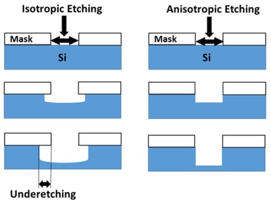
For understanding the direction of the micro-/nanostructure on the etched Si substrate surface, two basic chemical wet etching orientations are discussed: isotropic etching (orientation-independent) and anisotropic etching (orientation-dependent), as illustrated in Figure 1. In isotropic etching, the etchants H 2O 2 or HNO 3, which are considered as non-directional etchants, are applied to the Si substrate. During isotropic etching, a chemical reaction occurs that leads to the transportation of etchants to the sample surface and/or etching products away from the etched surface. This helps to remove the exposed areas of the Si substrate and, as a result, the sample is etched equally in all directions [22][23][24].
3. Applied Metal Nanoparticles in the MACE Technique
Silver is one of the most used noble metals, and several experimental studies were found in the literature where Ag was used as a catalyst in the MACE method. Li et al. presented a simple MACE method by creating a silver coating on the surface of the Si substrate in an aqueous solution of AgNO 3 (with 0.01 M molar ratio) and HF (with 2.3 M molar ratio). The etching was conducted with a thin Ag layer using oxidizing agents (H 2O 2, H 2O, and HF) at room temperature in the absence of light. Subsequently, the Ag particles were removed in the HNO 3 solution. This work aimed to identify the optimized fabrication parameters, including etching time, deposition time, and the molar ratio of oxidizing and aqueous solutions, to gain the best anti-reflective BSi surface. The results showed that the best experimental parameter for depositing AgNO 3:HF is 0.01:2.3 M, with a deposition time of 120 s. The optimized reaction parameters of etching time and molar ratios of HF: H 2O 2 are 5 m and 4.6:0.5 M, respectively. Moreover, they noted that the size of the nanowires should be within the range of 1–3 µm to stabilize or increase the antireflection capability of BSi [25]. Two main reactions happen during the etching: Si + 4Ag + + 6F − → 4Ag + SiF6 2− ,(6) 2Ag + H 2O 2 + 2H + → 2Ag + + 2H 2O. (7)
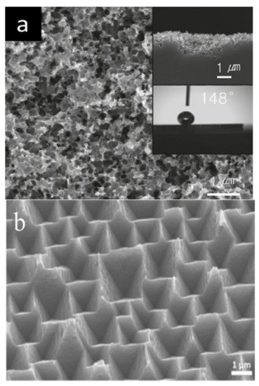
Lee et al. in 2010 observed that by using Cu as a catalyst, BSi nanostructures were etched randomly because Cu nanoparticles do not fallow any specific direction while etching [26]. In the same vein, Park et al. in 2018 investigated the Cu MACE experiment and found that if the ratio of HF is significantly less during the etching time, the rate of etching is too low to properly form the textured surface. The same thing happened when the etching time was too short. When they increased the etching time along with increasing the ratio of HF solution, they found the lowest reflectance. The reason behind this is the formation of an oxide film by HF at the interface of Si and Cu particles during the etching time, which helped the Cu particles to penetrate deeply enough to form a dense and minute pore structure, as shown in Figure 2a [27].
Lua and Barron in 2014 proposed a one-step MACE using Cu as a metal catalyst [28]. In their experimental study, they used a solution mixed with Cu 2+ and H 3PO 3 where inverted pyramid-shaped structures were developed on the BSi surface. These shapes appeared because of the low reduction potentials of Cu 2+ that caused the Si etching to happen with Si{100} and Si{110} directions simultaneously. Chen et al. concluded that in a Cu-etched BSi surface, the textures are inverted pyramid-shaped because of the low redox potential of Cu nanoparticles and the anisotropic etching behavior. Figure 2b shows the SEM images of the inverted pyramidal structure surface layer of the Si wafer [29]. However, as mentioned, Lee et al. ’s experimental result with Cu nanoparticles resulted in the formation of hierarchical synthesized rough Si surfaces. This happened because of the occurrence of shallow pits on the Si surface from relatively low redox potentials [30][31].
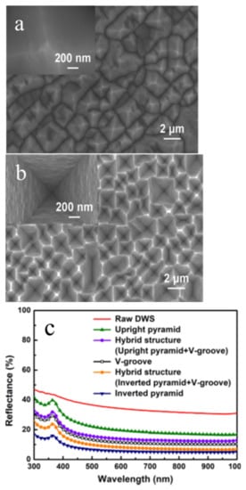
Moreover, to reduce defects in micro-structured textured surfaces with the minimum reflectivity of a Cu-etched BSi surface, Zhao et al. proposed that the Cu catalyst is better suited with Si{110} direction crystalline planes [32]. In their experimental study, the morphologies of the BSi surface were transformed from the upright pyramid-shaped to the inverted pyramid-shaped structure via increasing deposition concentration and agglomeration degree of Cu nanoparticles, as shown in Figure 3 .
4. Conclusions
References
- Zuo, Z.; Cui, G.; Shi, Y.; Liu, Y.; Ji, G. Gold-thickness-dependent Schottky barrier height for charge transfer in metal-assisted chemical etching of silicon. Nanoscale Res. Lett. 2013, 8, 193.
- Akan, R.; Parfeniukas, K.; Vogt, C.; Toprak, M.; Vogt, U. Reaction control of metal-assisted chemical etching for silicon-based zone plate nanostructures. RSC Adv. 2018, 8, 12628–12634.
- Kim, J.; Kim, Y.; Choi, S.; Lee, W. Curved Silicon Nanowires with Ribbon-like Cross Sections by Metal-Assisted Chemical Etching. ACS Nano 2011, 5, 5242–5248.
- Venkatesan, R.; Arivalagan, M.; Venkatachalapathy, V.; Pearce, J.; Mayandi, J. Effects of silver catalyst concentration in metal assisted chemical etching of silicon. Mater. Lett. 2018, 221, 206–210.
- Huang, Z.; Zhang, X.; Reiche, M.; Liu, L.; Lee, W.; Shimizu, T.; Senz, S.; Gösele, U. Extended Arrays of Vertically Aligned Sub-10 nm Diameter Si Nanowires by Metal-Assisted Chemical Etching. Nano Lett. 2008, 8, 3046–3051.
- Zheng, H.; Han, M.; Zheng, P.; Zheng, L.; Qin, H.; Deng, L. Porous silicon templates prepared by Cu-assisted chemical etching. Mater. Lett. 2014, 118, 146–149.
- Volovlikova, O.; Gavrilov, S.; Lazarenko, P.; Kukin, A.; Dudin, A.; Tarhanov, A. Influence of Etching Regimes on the Reflectance of Black Silicon Films Formed by Ni-Assisted Chemical Etching. Key Eng. Mater. 2019, 806, 24–29.
- Huang, Z.; Geyer, N.; Werner, P.; de Boor, J.; Gösele, U. Metal-Assisted Chemical Etching of Silicon: A Review. Adv. Mater. 2010, 23, 285–308.
- Li, X.; Bohn, P. Metal-assisted chemical etching in HF/H2O2 produces porous silicon. Appl. Phys. Lett. 2000, 77, 2572–2574.
- Zhang, P.; Jia, R.; Tao, K.; Jiang, S.; Dai, X.; Sun, H.; Jin, Z.; Ji, Z.; Liu, X.; Zhao, C.; et al. The influence of Ag-ion concentration on the performance of mc-Si silicon solar cells textured by metal assisted chemical etching (MACE) method. Sol. Energy Mater. Sol. Cells 2019, 200, 109983.
- Hildreth, O.; Lin, W.; Wong, C. Effect of Catalyst Shape and Etchant Composition on Etching Direction in Metal-Assisted Chemical Etching of Silicon to Fabricate 3D Nanostructures. ACS Nano 2009, 3, 4033–4042.
- Wang, Y.; Liu, Y.; Liang, H.; Mei, Z.; Du, X. Broadband antireflection on the silicon surface realized by Ag nanoparticle-patterned black silicon. Phys. Chem. Chem. Phys. 2013, 15, 2345.
- Han, H.; Huang, Z.; Lee, W. Metal-assisted chemical etching of silicon and nanotechnology applications. Nano Today 2014, 9, 271–304.
- Liu, R.; Zhang, F.; Con, C.; Cui, B.; Sun, B. Lithography-free fabrication of silicon nanowire and nanohole arrays by metal-assisted chemical etching. Nanoscale Res. Lett. 2013, 8, 155.
- Wu, Y.; Gao, F.; Wu, H.; Liu, X.; Zheng, X.; Liu, S.; Wang, H.; Zhou, S.; Li, F. The effects of Ag particle morphology on the antireflective properties of silicon textured using Ag-assisted chemical etching. J. Alloy. Compd. 2016, 670, 156–160.
- Pakhuruddin, M.; Huang, J.; Dore, J.; Varlamov, S. Enhanced light-trapping in laser-crystallised silicon thin-film solar cells on glass by optimised back surface reflectors. Sol. Energy 2017, 150, 477–484.
- Xie, T.; Schmidt, V.; Pippel, E.; Senz, S.; Gösele, U. Gold-Enhanced Low-Temperature Oxidation of Silicon Nanowires. Small 2008, 4, 64–68.
- Werner, P.; Büttner, C.; Schubert, L.; Gerth, G.; Zakarov, N.; Gösele, U. Gold-enhanced oxidation of silicon nanowires. Int. J. Mater. Res. 2007, 98, 1066–1070.
- Büttner, C.; Zakharov, N.; Pippel, E.; Gösele, U.; Werner, P. Gold-enhanced oxidation of MBE-grown silicon nanowires. Semicond. Sci. Technol. 2008, 23, 075040.
- Toofan, M.; Toofan, J. A Brief Review of the Cleaning Process for Electronic Device Fabrication. Dev. Surf. Contam. Clean. 2015, 185–212.
- Lehmann, V. The Electrochemistry of Silicon; Wiley-VCH: Weinheim, Germany, 2010.
- Veenendaal, E.V.; Sato, K.; Shikida, M.; Nijdam, A.; Suchtelen, J.V. Micro-morphology of single crystalline silicon surfaces during anisotropic wet chemical etching in KOH: Velocity source forests. Sens. Actuators A Phys. 2001, 93, 232–242.
- Bean, K. Anisotropic etching of silicon. IEEE Trans. Electron Devices 1978, 25, 1185–1193.
- Seidel, H.; Csepregi, L.; Heuberger, A.; Baumgärtel, H. Anisotropic etching of crystalline silicon in alkaline solutions: I. Orientation dependence and behavior of passivation layers. J. Electrochem. Soc. 1990, 137, 3612.
- Li, S.; Ma, W.; Chen, X.; Xie, K.; Li, Y.; He, X.; Yang, X.; Lei, Y. Structure and antireflection properties of SiNWs arrays form mc-Si wafer through Ag-catalyzed chemical etching. Appl. Surf. Sci. 2016, 369, 232–240.
- Lee, J.; Choi, S.; Park, S. Extremely Superhydrophobic Surfaces with Micro- and Nanostructures Fabricated by Copper Catalytic Etching. Langmuir 2011, 27, 809–814.
- Park, J.E.; Cho, Y.H.; Kang, S.; Hong, H.K.; Kim, D.S.; Lim, D. Effect of Cu-Assisted Chemical Etching for Black Silicon. In Proceedings of the IEEE 7th World Conference on Photovoltaic Energy Conversion (WCPEC) (A Joint Conference of 45th IEEE PVSC, 28th PVSEC & 34th EU PVSEC), Waikoloa Village, HI, USA, 10–15 June 2018; pp. 1047–1050.
- Lu, Y.; Barron, A. Anti-reflection layers fabricated by a one-step copper-assisted chemical etching with inverted pyramidal structures intermediate between texturing and nanopore-type black silicon. J. Mater. Chem. A 2014, 2, 12043.
- Chen, W.; Liu, Y.; Yang, L.; Wu, J.; Chen, Q.; Zhao, Y.; Wang, Y.; Du, X. Difference in anisotropic etching characteristics of alkaline and copper based acid solutions for single-crystalline Si. Sci. Rep. 2018, 8, 3408.
- Chern, W.; Hsu, K.; Chun, S.I.; Azeredo, B.P.D.; Ahmed, N.; Kim, K.; Zou, J.; Fang, N.; Ferreira, P.; Li, X. Nonlithographic Patterning and Metal-Assisted Chemical Etching for Manufacturing of Tunable Light-Emitting Silicon Nanowire Arrays. Nano Lett. 2010, 10, 1582–1588.
- Peng, K.; Lu, A.; Zhang, R.; Lee, S. Motility of Metal Nanoparticles in Silicon and Induced Anisotropic Silicon Etching. Adv. Funct. Mater. 2008, 18, 3026–3035.
- Zhao, Y.; Liu, Y.; Chen, W.; Wu, J.; Chen, Q.; Tang, H.; Wang, Y.; Du, X. Regulation of surface texturization through copper-assisted chemical etching for silicon solar cells. Sol. Energy 2020, 201, 461–468.

