Your browser does not fully support modern features. Please upgrade for a smoother experience.
Submitted Successfully!
 +1 credit
Thank you for your contribution! You can also upload a video entry or images related to this topic.
For video creation, please contact our Academic Video Service.
| Version | Summary | Created by | Modification | Content Size | Created at | Operation |
|---|---|---|---|---|---|---|
| 1 | Antonio d'Alessandro | + 1210 word(s) | 1210 | 2021-09-24 10:58:08 | | | |
| 2 | Conner Chen | Meta information modification | 1210 | 2021-10-25 11:02:35 | | | | |
| 3 | Conner Chen | Meta information modification | 1210 | 2021-11-02 07:09:37 | | |
Video Upload Options
We provide professional Academic Video Service to translate complex research into visually appealing presentations. Would you like to try it?
Cite
If you have any further questions, please contact Encyclopedia Editorial Office.
D'alessandro, A. Liquid Crystal Waveguide Structures. Encyclopedia. Available online: https://encyclopedia.pub/entry/15304 (accessed on 25 July 2026).
D'alessandro A. Liquid Crystal Waveguide Structures. Encyclopedia. Available at: https://encyclopedia.pub/entry/15304. Accessed July 25, 2026.
D'alessandro, Antonio. "Liquid Crystal Waveguide Structures" Encyclopedia, https://encyclopedia.pub/entry/15304 (accessed July 25, 2026).
D'alessandro, A. (2021, October 22). Liquid Crystal Waveguide Structures. In Encyclopedia. https://encyclopedia.pub/entry/15304
D'alessandro, Antonio. "Liquid Crystal Waveguide Structures." Encyclopedia. Web. 22 October, 2021.
Copy Citation
Liquid crystal materials can be used to make either a core, in which light beams can be confined, or a cladding of optical waveguides.
liquid crystals
optical waveguides
optoelectronics
integrated optics
1. Nematic LC Confined in SiO2/Si V-grooves
A channel waveguide can be obtained by infiltrating a nematic liquid crystal (LC) in a SiO2/Si groove as shown in Figure 1a. The Indium Tin Oxide (ITO) layer and the n-Si substrate act as electrodes to apply an external electric field. A silicon V-groove is made by exploiting anisotropic etching of silicon. Typical groove width ranges from 5 to 15 µm. A native thermal oxide SiO2, obtained in an oven at about 1100 °C acts as a low index cladding, considering that a nematic LC has a refractive index higher than 1.45. The V-groove is fabricated by means of a micromachining process whose details are described in ref [1].
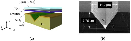
Figure 1. Optical waveguide made of LC infiltrated in a SiO2/Si V-groove: (a) Three-dimensional exploded schematic, showing the orientation of the nematic LC molecules along the V-groove; (b) Electron microscope scanning of a SiO2/Si V-groove.
Figure 1b shows a scanning electron microscope picture of the V-groove in which smoothness of SiO2/Si surfaces is able to minimize defects in the embedded LC molecules, consequently attenuating light scattering in the final LC waveguide.
The etching of Si creates a V-groove with an angle α = 54.7° using (100) Si wafer as schematically shown in Figure 2a. A glass cover of 0.5 mm is then placed on top of the V-groove [2]. A D263 borosilicate glass substrate is used with a refractive index nD263 = 1.516 (at the at wavelength λ = 1.55 µm) intermediate between the values of the extraordinary and the ordinary refractive index of the LC used, such as E7 (ne = 1.69, no = 1.5 at wavelength λ = 1.55 µm), which allows the creation of an optical switch [2]. A thin film of Nylon 6 is spanned and rubbed on top of the ITO film, to align the LC along the groove. Nematic LC E7 in the isotropic phase is infiltrated in the covered V-groove by capillarity in vacuum at 80 °C and then cooled down to the room temperature. Figure 3b shows the orientation of nematic LC molecules, whose tilt angle θ is controlled by the applied voltage between the ITO and n-Si.
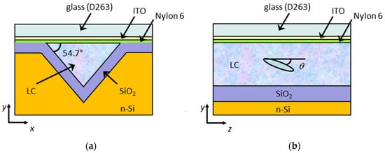
Figure 2. Schematic images of an LC waveguide in SiO2/Si groove: (a) cross-section indicating the etching angle of the Si groove; (b) longitudinal section showing the orientation of the nematic LC molecules under applied electric field between ITO and n-Si.
Light is coupled to LC waveguides in Si/SiO2 grooves, referred to as LCW (Liquid Crystal Waveguide), by fibre butt-coupling, as shown in Figure 3. Since LC-NOA61 interface was used, total coupling losses, including input and output, of 4.5 dB or better were measured, as a result of minimization of LC molecular random orientation representing a source of light scattering at the input and output faces of the LCW, which determined higher coupling losses in previous samples without LC-NOA61 interface [3]. Propagation losses resulted to be about 6 dB/cm which can be further lowered by using photoalignment techniques, able to improve the optical quality of the LCW [4][5].
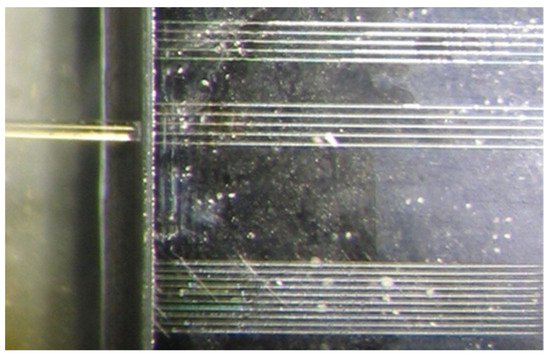
Figure 3. Picture of a single-mode optical fiber which is butt-coupled to a chip, including a set of LC waveguides on SiO2/Si grooves. Waveguide width is 8–12 µm.
2. Nematic LC in PDMS Waveguides
Optical waveguides can be made by infiltrating a nematic LC in polydimethylsiloxane (PDMS) channels by capillarity. Such waveguides are referred as LC:PDMS waveguides. Use of PDMS is motivated since it is a material often used for microfluidic applications with high optical quality [6]. PDMS is optical transparent, with low surface energy in the range of 20–23 mJ/m2 at 20 °C [7], low dielectric constant in the range of 2.32–2.40 [8] and Young’s modulus, which is between 0.57 MPa and 3.7 MPa [9], and thermally and optically enabled polymerization. PDMS is also reliable for soft lithographic fabrication of many microfluidic and micro-optical devices [10].
Flexibility is another attractive feature of PDMS which is effectively used in robotics, automation, consumer electronics and in novel applications, such as health care and biomedical technologies. PDMS is used in optical interconnections for datacom applications to replace metallic connections whose performance in terms of bit rate are very low and suffer problems related to high heat dissipation [11].
PDMS channels to be filled with a nematic LC are fabricated by the cast and moulding technique involving several technological phases as shown in Figure 4 and described in ref. [12].
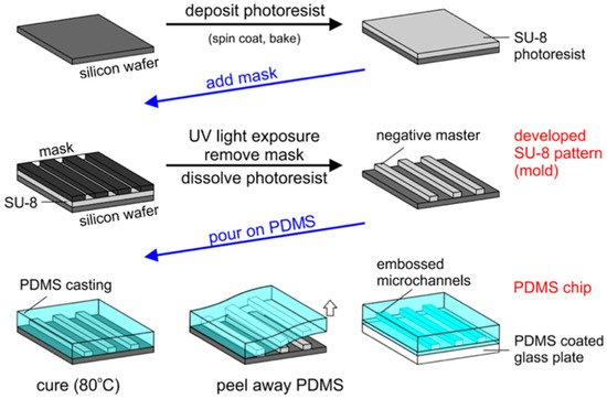
Figure 4. Technological phases to make PDMS microchannels used obtain LC:PDMS waveguides.
The PDMS channels are filled with a nematic LC by capillarity which results in homeotropically alignment as shown in Figure 5a. Homeotropic alignment of LC is due to the hydrophobic characteristic of the PDMS inner surface. A fabricate sample including LC:PDMS waveguides with widths of 8, 10 and 15 µm is reported in Figure 5b. The optical characterization to check the LC alignment in the LC:PDMS waveguides is performed using a polarized microscope. Polarized light is transmitted through the channels, revealing the homeotropic arrangement of the LC molecules. Such orientation of the LC is proven by the black part in the central region for the waveguides indicating that polarization of input light is not changed when transmitted through the LC and is stopped by the crossed analyser, as it can be observed in Figure 5c. Light leaks through the edges of the waveguides because of the optical retardation induced by the LC molecules homeotropically aligned on the vertical sides of the PDMS channels.
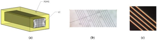
Figure 5. LC:PDMS waveguides: (a) oriented LC molecules inside the PDMS channel; (b) PDMS chip with optical waveguides with widths of 8, 10 and 15 µm; (c) image of LC:PDMS waveguides with a width of 10 µm observed under the microscope in transmission.
LC molecular orientation inside the PDMS channel induces a refractive index distribution which determines polarization-independent light propagation [12]. Green laser light at a wavelength of 532 nm and red light using an He-Ne laser source at a wavelength of 632.8 nm were efficiently fibre butt-coupled to the LC:PDMS waveguide as shown in Figure 6a. Propagation in the C-band was also studied using a tunable laser source between 1510 nm and 1590 nm. Light transmission versus polarization orientation was measured using a set-up including a polarization controller, consisting of a half-wave plate between two quarter-wave plates, an optical power meter and a polarizer at the output of the waveguide. It has been observed that light polarization does not vary as it propagates along the LC:PMDS channel for any polarization at the input. A polarization differential loss of only 0.3 dB, as shown in Figure 6b, was measured with propagation losses of about 8 dB/cm.
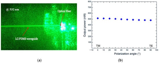
Figure 6. Propagation properties of an LC:PDMS waveguide with a width of 15 µm: (a) green laser light (wavelength = 532 nm) beam butt−coupled by using a single mode optical fiber of 125 µm; (b) output power versus polarization at a wavelength of 1550 nm.
It is possible to control LC:PDMS waveguides by means of coplanar electrodes. Preliminary measurements show that LC molecules can be switched by applying a square voltage of 1 kHz with an amplitude of about 2 V. In this case, only change of modal propagation was affected without a substantial light transmission of light, since the core refractive index remains above the PDMS refractive index. By choosing a PDMS with a refractive index intermediate between the ordinary and the extraordinary refractive of the LC, light modulation or switching is possible.
References
- Donisi, D.; Bellini, B.; Beccherelli, R.; Asquini, R.; Gilardi, G.; Trotta, M.; D’Alessandro, A. A Switchable Liquid-Crystal Optical Channel Waveguide on Silicon. IEEE J. Quantum Electron. 2010, 46, 762–768.
- Bellini, B.; d’Alessandro, A.; Beccherelli, R. A method for butt-coupling optical fibers to liquid crystal planar waveguides. Opt. Mater. 2007, 29, 1019–1022.
- Chigrinov, V.G.; Kozenkov, V.M.; Kwok, H.-S. Photoalignment of Liquid Crystalline Materials: Physics and Applications; Wiley: New York, NY, USA, 2008.
- Schadt, M. Liquid creystal displays, LC materials and LPP photoalignment. Mol. Cryst. Liq. Cryst. 2017, 320, 253–268.
- Duffy, D.C.; McDonald, J.C.; Schueller, O.J.A.; Whitesides, G.M. Rapid Prototyping of Microfluidic Systems in Poly(dimethylsiloxane). Anal. Chem. 1998, 70, 4974–4984.
- Lee, L.-H. Enhancement of surface wettability of adhesive silicone rubber by oxidation. J. Adhes. 1972, 4, 39–49.
- Du, P.; Lin, X.; Zhang, X. Dielectric constants of PDMS nanocomposites using conducting polymer nanowires. In Proceedings of the 16th International Solid-State Sensors, Actuators and Microsystems Conference, Beijing, China, 5–9 June 2011; pp. 645–648.
- Wang, Z.; Volinsky, A.A.; Gallant, N.D. Crosslinking effect on polydimethylsiloxane elastic modulus measured by custom-built compression instrument. J. Appl. Polym. Sci. 2014, 131, 41050.
- McDonald, J.C.; Duffy, D.C.; Anderson, J.R.; Chiu, D.T.; Wu, H.; Schueller, O.J.; Whitesides, G.M. Fabrication of microfluidic systems in poly(dimethylsiloxane). Electrophoresis 2000, 21, 27–40.
- Missinne, J.; Kalathimekkad, S.; Van Hoe, B.; Bosman, E.; Vanfleteren, J.; Van Steenberge, G. Stretchable optical waveguides. Opt. Express 2014, 22, 4168–4179.
- d’Alessandro, A.; Martini, L.; Gilardi, G.; Beccherelli, R.; Asquini, R. Polarization-Independent Nematic Liquid Crystal Waveguides for Optofluidic Applications. IEEE Photonics Technol. Lett. 2015, 27, 1709–1712.
More
Information
Contributor
MDPI registered users' name will be linked to their SciProfiles pages. To register with us, please refer to https://encyclopedia.pub/register
:
View Times:
1.4K
Revisions:
3 times
(View History)
Update Date:
02 Nov 2021
Table of Contents


Notice
You are not a member of the advisory board for this topic. If you want to update advisory board member profile, please contact office@encyclopedia.pub.
OK
Confirm
Only members of the Encyclopedia advisory board for this topic are allowed to note entries. Would you like to become an advisory board member of the Encyclopedia?
Yes
No
${ textCharacter }/${ maxCharacter }
Submit
Cancel
Back
Comments
${ item }
|
${ item.createdUser.fullName }
${ item.createdAt }
${ item.vote }
${ item.reply }
Delete
${ reply.createdUser.fullName }
${ reply.createdAt }
${ reply.vote }
Delete
There is no reply to this comment~
${ item.replyTextCharacter }/${ item.replyMaxCharacter }
Submit
Cancel
More
No more~
There is no comment~
${ textCharacter }/${ maxCharacter }
Submit
Cancel
${ selectedItem.replyTextCharacter }/${ selectedItem.replyMaxCharacter }
Submit
Cancel
Confirm
Are you sure to Delete?
Yes
No