 +1 credit
| Version | Summary | Created by | Modification | Content Size | Created at | Operation |
|---|---|---|---|---|---|---|
| 1 | Mohammad Nur E Alam | + 2344 word(s) | 2344 | 2019-10-23 06:14:57 | | | |
| 2 | Amber Yao | -1 word(s) | 2343 | 2019-10-24 05:34:28 | | | | |
| 3 | Amber Yao | Meta information modification | 2343 | 2019-11-01 07:04:41 | | | | |
| 4 | Vivi Li | -10 word(s) | 2333 | 2020-10-30 04:35:41 | | |
Video Upload Options
We report on the development of several different thin-film material systems prepared by RF magnetron sputtering at Edith Cowan University nanofabrication labs. While focusing on the RF sputtering process optimizations for new or the previously underexplored material compositions and multilayer structures, we disclose several unforeseen material properties and behaviours. We communicate research results related to the design, prototyping, and practical fabrication of high-performance magneto-optic (MO) materials, oxide based sensor components, and transparent heat regulation coatings for advanced construction and solar windows.
1. Introduction
Magnetron sputter deposition is one of the most common technologies used to grow thin film materials and coatings for various existing and modern nano-technological applications. Sputter deposition of thin films has a long track record of development history in vacuum technology since the 1800s. Many dedicated research groups and scholars were involved in the development of the modern phase of magnetron sputtering technology, although the journey of the magnetron sputtering process is still considered far from its ultimate development[1][2][3][4][5][6] . However, nowadays the magnetron sputtering is considered one of the most effective processes for the deposition of a wide range of high-quality thin-film materials either in single or multilayer form, including metals, dielectrics, metal oxides of complex stoichiometry, and nanoparticles. A vast number of sputtered material types were shown to be suitable for various existing and emerging nanotechnology-related applications, and attractive for many rapidly growing diverse market sectors. Sputtering processes allow to deposit thin-film materials either on bare substrates or on top of any structured systems, e.g. photonic or magneto-photonic crystals, usually without having any unpredictable thickness uniformity or stoichiometry issues with the grown films. Thin-film materials, especially radio frequency (RF) magnetron sputtered thin films were originally considered useful mainly in electronics and semiconductor devices, however, sputtered thin films have also been found to be applicable within a wide range of fields such as optoelectronics, energy, mechanical/chemical, optical coatings, life sciences, and others [7][8][9][10][11][12][13][14][15][16][17][18]. In this nano-technological era, the sputter-deposition of thin films becomes a rather universal and actively growing field of human endeavour, integrating the fundamental and important scientific areas of research, process development, deposition-system design, and new product manufacturing. This trend is expected to continue into the periods extending far into the near future. Figure 1 presents a wide range of possible application areas of sputtered thin films for the continued exploration by future generations. The sputtered thin-films market is expected to grow globally at a significant rate due to the demand for miniaturization of thin-film related technologies, devices, and products necessary for modern nano-technological applications[19].
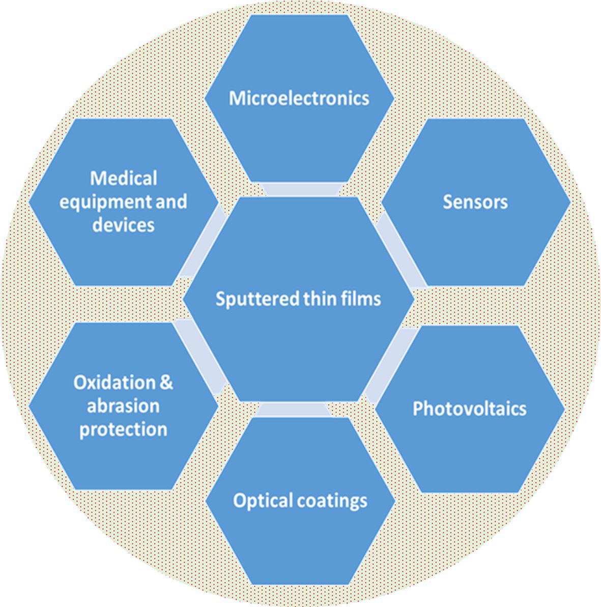
Figure 1. Spectrum of modern nano-technological application areas reliant on sputtered thin-film materials.
In this study, we present the experimental results selected from a decade-long lab-based work, during which the RF sputtering synthesis of different thin-film material types and multilayer structures have been explored extensively. We also present the specific material development results and functional material properties of interest for several specific applications.
2. Garnets, Garnet-oxide composites (GOCs), and Multilayer Thin-Film Structures
Natural garnets are popular as gemstones, but when they are engineered either by modifying their stoichiometry or by adjusting the fabrication process, they can possess extra-ordinary multifunctional properties that make them attractive for various applications e.g. integrated photonic circuits and devices. Through nano-engineering, garnet thin films can be controlled, at the atomic level, to attain naturally-unachievable photonic and magnetic properties that open the way towards the development of magnetophotonic and magneto-plasmonic crystals (MPCs) for a wide range of applications, including telecommunication, biomedicine, digital forensics, sensing and data processing. Since the last decade, a number of highly bismuth (Bi) substituted iron garnet thin-film material systems including garnet-oxide and garnet-garnet nano-composite derivatives, have been synthesized, their sputtering process parameters optimized, and many studies of the optical, magnetic and magneto-optical properties were reported by our group at Edith Cowan University (ECU)[16]. Here, we like to present the recently obtained results on the optical constants of RF sputtered highly Bi-substituted iron-garnet precursors of nominal composition type Bi2Dy1Fe4Ga1O12 (BiDyIG) and garnet-oxide composites (GOC), together with a glimpse of the previously best-achieved MO properties in thin garnet films of similar compositions. We also disclose the unconventional hysteresis loop shapes that have been discovered in GOC-based all-garnet multilayer structures by our group, observed in 2015 for the first time[20].
Garnet-oxide composite and GOC-based all-garnet multilayer structures films were prepared by RF magnetron sputtering on Corning Eagle XG glass substrates. All these thin films and multilayer structures were deposited at room temperature in pure argon (Ar) plasma. After the deposition process, all of these films and structures were in an amorphous state, essentially representing the garnet precursors, which needed subsequent crystallization. Crystallization of the garnet phases was achieved using high-temperature oven-annealing processes in ambient air atmosphere, optimized for each material type. During the deposition of both the amorphous-phase garnet films and garnet-oxide composites, the oxygen loss occurs, and manifests in the increased optical absorption in the as-deposited films, compared to the expected material data. This oxygen loss, and also its compensation, can be confirmed by the reduced optical absorption and by the improved optical properties seen in annealed garnet layers, which closely match these reported for garnets synthesized by other techniques (e.g. liquid-phase epitaxy or pulsed-laser deposition).
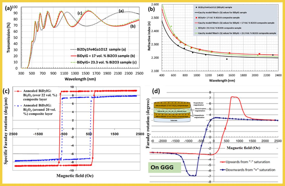
Figure 2. Development and performance of garnet, garnet-oxide composite and GOC-based all-garnet multilayer structures.
From Fig. 2 (a, b), it can be seen that the volumetric fraction of excess Bi2O3 introduced into the BiDyIG system helps increase the refractive index of the composite films, and this also shifts the absorption edge towards the shorter wavelength region. The refractive index (n) was found to be in the range of 2.2-2.6 in the visible region, and it decreases with increasing wavelength. Note that there are always significant differences that exist between the optical constants of the crystallized garnets and oxide-mix-based amorphous precursor layers. On the other hand, the effects of introducing excess Bi2O3 into the iron-garnet-type systems can lead to obtaining the practically perfectly “square” shapes of hysteresis loops, observed in the crystallized GOC MO films (Fig. 2c) with strong perpendicular magnetic anisotropy, high (close to 100 %) remnant magnetization, and featuring very sensitive magnetic switching behaviours.
We observed an unconventional and remarkable magnetic switching properties for the first time in RF magnetron sputtered all-garnet multilayer thin-film structures, in which the magneto-soft layers were sandwiched in-between two magneto-hard garnet material layers of identical composition type (Fig. 2d). A notable feature of this hysteresis loop behavior was the presence of an “intermediate saturation” state exhibiting the maximum Faraday rotation, which then was followed by conventional magnetization saturation state with reduced Faraday rotation, at increasing external magnetic fields above about 1 kOe. The final saturated Faraday rotation was observed at near 1.6 kOe, at below 50% of the maximum Faraday rotation angle seen at smaller fields. To the best of our knowledge, no prior (or later) reports of similar magnetic switching behaviours observed in any thin-film materials, can be found in the published literature. These exchange-coupled all-garnet multilayer structures demonstrated an attractive combination of optical and magnetic properties, and are of interest for emerging applications in optical sensors and isolators, ultrafast nanophotonics, magneto-plasmonics and possibly spintronics.
3. Ruthenium-Oxide Based Cost-Effective Sensor Electrodes
Sputter-deposition process parameters are well known to affect the growth and properties of thin-film materials, especially the oxide-based thin-film materials. Therefore, it is necessary to optimize the sputter-deposition process parameters and it is important to control the materials properties for many application-specific oxide-based thin-films. For example, ruthenium oxide (RuO2) thin film based sensing electrodes have been developed and their performance versus the process parameters were studied extensively. RuO2 based sensor electrodes are suitable for use in various sensing devices, such as pH sensing, cryogenic temperature sensing, and even in bio-sensing applications. We present the growth of durable (and therefore cost-effective) electrodes (RuO2 thin-film electrodes) on flexible and rigid substrates, along with the pH and temperature sensing performance of these electrodes.
RuO2 thin-film electrodes (potentiometric, interdigitated and resistive) were deposited directly onto two different substrate materials (alumina and polyimide), using RF magnetron sputtering from a metal-oxide (RuO2) ceramic target, at room temperature. Several batches of RuO2 thin films were grown on photo-lithographically obtained custom shaped electrodes, using a 4 mTorr chamber pressure and 1:1 Ar: O2 gas ratio.
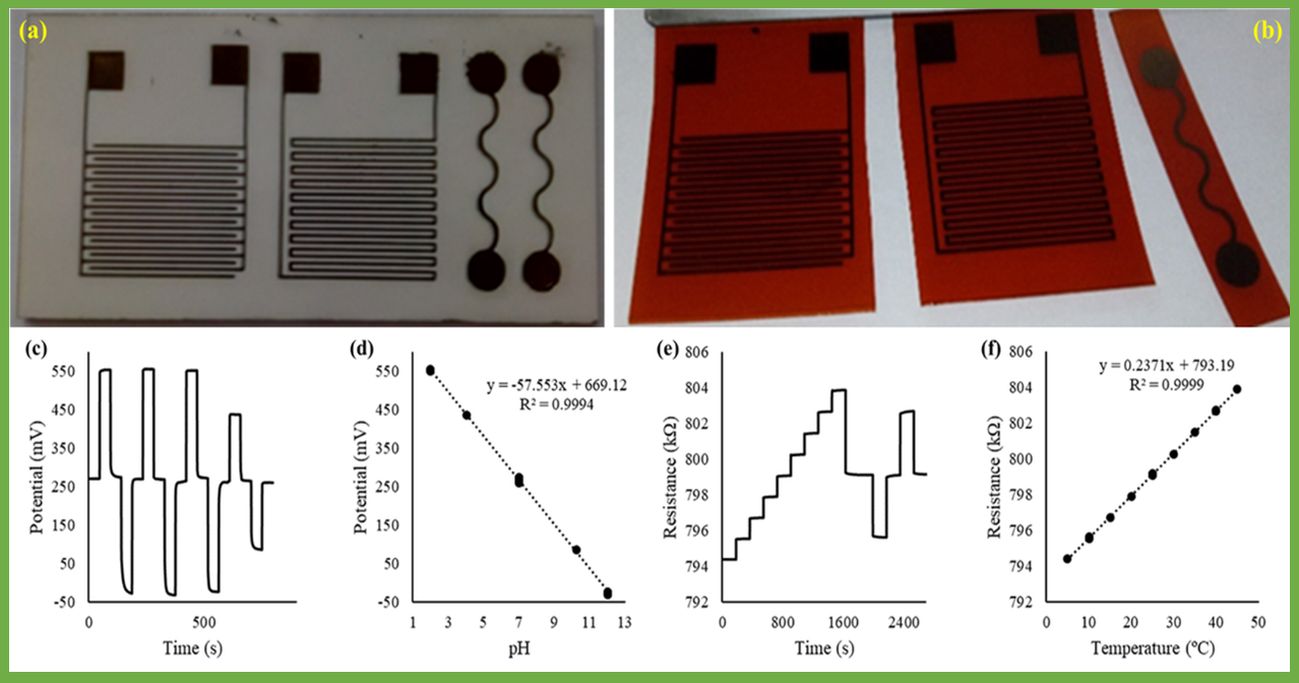
Figure 3. Design, fabrication and performance (testing results) of RuO2 thin-film based electrodes.
It has been found experimentally that the polyimide-based electrodes showed excellent performance when used as potentiometric pH electrode (vs. Ag|AgCl|KCl reference electrode), exhibiting a reversible (±3.9 mV), linear (R2=0.9994) and Nernstian (57.5 mV/pH) pH response, as shown in Fig. (3 c & d). The polyimide resistive and interdigitated electrodes failed when used as conductivity and temperature sensors, due to gradual delamination. However, the alumina-based resistive temperature sensor exhibited a reversible (± 0.01 °C) linear (R2=0.9999) response, as shown in Fig. (3 e & f). To summarize, durable metallic RuO2 thin films could only be deposited with a chamber pressure ≥ 4 mTorr with a close to a (1:1) argon/oxygen content ratio in the chamber. RuO2 films deposited at pressures lower than 4 mTorr produced powdery films that rapidly delaminate from all substrates. The improved durability of these RuO2 electrodes allows for the development of reliable sensors, potentially for miniaturised applications or where conventional glass probes are not suitable, such as biomedical applications.
4. Metal-Dielectric Nanocomposite and Multilayer Building Blocks for Solar and Thermal Radiation Filters
The development of modern energy-efficient glass and window products requires specialized thin-film coatings containing ultra-thin silver (Ag) layer(s) to filter or reflect the infrared and far-infrared (thermal) radiation components of the solar spectrum, thus reducing the energy consumption in buildings. The deposition of the ultra-thin Ag layers with low surface roughness and high uniformity is the key to achieving the required application-specific optical properties. However, the deposition of ultra-thin (less than 20 nm) Ag layers often results in multiple quality issues, such as forming morphologically uneven nano-islands, quick oxidation (happening during the deposition of the subsequent material layer), and possibly even destroying the morphological quality in any dielectric material layer(s) deposited on top of these nanoisland-shaped, incontiguous ultra-thin Ag layers. All the above-mentioned practical issues related to the ultra-thin Ag layer growth significantly affect the optical performance of multilayer metal-dielectric thin-film structures.
We have prepared co-sputtered metal-dielectric nanocomposites (MDC) by developing co-sputtering processes for the Ag-MgF2 system, with various volumetric contents of the dielectric phase added to the metal to overcome the issues related to the difficulties of forming quality ultra-thin Ag layers. We have also developed MDC-containing multilayer structures, and their characterisation results suggest that MDC layers can replace the pure-metal layers in multilayer optical coatings, thus offering a new possibility to design and fabricate highly durable and environmentally-stable coatings (low-emissivity and/or the heat-mirror-type) on glass substrates, suitable for solar and thermal regulation technologies.
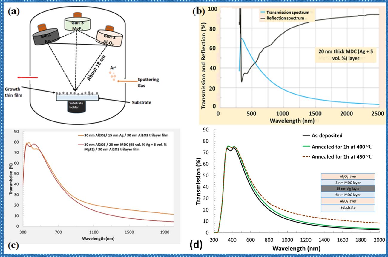
Figure 4. Design, development and performance characterization (results at a glance) for metal/dielectric composite (MDC) and MDC-based multilayer structures.
Figure 4 presents the co-sputtering geometry of the growth of metal-dielectric (Ag/MgF2) nano-composites together with the design, development and performance characterization (results at a glance) for metal/dielectric composite (MDC) and MDC based multilayer structures. It can be noted that the transmission peak in this Ag+MgF2 (5 vol. %) composite layer exhibited short-wavelength transmission and reflection features similar to the Ag layer of the same thickness (Fig. 4b). This, together with a high reflectivity across near-infrared, indicates that the addition of 5 vol. % MgF2 into the Ag layer during the co-sputtering process can potentially improve the coating adhesion and stability aspects without compromising the plasmonics metal properties.
The transmission spectra of a tri-layer MDC structure (as shown in Fig. 4c, compared to that of a typical Ag layer within a DMD structure) revealed that it is possible to use a comparatively thicker (25 nm MDC) layer instead of a pure 15 nm Ag layer. MDC based multilayer structures showed better thermal radiation filtering performance without compromising the visible spectral transmission, whilst avoiding any potential layer morphology-related issues that usually affect ultrathin (thinner than about 17 nm) layers. Experimental investigations revealed that the MDC based structures also demonstrated a much lower thermal emissivity whilst maintaining the same superior visible transmission, compared to the silver-based coatings.
The design variations, material intercompatibility, durability and thermal stability properties of the MDC-based coatings were investigated by preparing several different types of test multilayers (up to five-layer structures). One of the examples (as shown in Fig. 4d) represents a more complex generalized MDC-type multilayer building block, which was subjected to extensive thermal stability (dry heat exposure) tests. The performance of the developed structure (before and after the heat exposure in an air-filled lab oven) shows that the optical properties are comparable to some of the conventional multilayer structures containing pure Ag layers. It can be seen clearly that the transmission spectra were found to be only slightly changed at temperatures near 400 °C, which confirms that the very thin MDC barrier layers can play a vital role in protecting the ultra-thin core Ag layers within the multilayer structures. This confirms that the MDC layers can be used to enable arbitrarily complex high-stability low-E, heat-mirror, or filter-type optical coating designs of high spectral selectivity, on a range of optical substrates.
5. Conclusions
We demonstrate a range of material system design possibilities for multiple practical applications provided by fine-tuning the RF magnetron sputtering technologies. We established numerous sputtering-based thin-film material synthesis processes at ECU, aiming at incorporating these optical materials into functional devices for sensing, optical spectra shaping, polarisation control, magnetic switching, and magnetic field visualization, among others. Several previously unforeseen and underexplored properties and behaviours have been identified in functional materials and structures deposited by sputtering. Among these are the unconventional hysteresis loop behaviour first observed in nanocomposite-based magneto-optic garnet multilayers, where an intermediate saturation-type magnetization state between ~ 700-1100 Oe existed. Additionally, we have demonstrated a rather high (up to >400 °C) thermal exposure (dry heat) stability in nano-engineered metal-dielectric multilayers. A cost-effective approach to the development of ruthenium oxide-based pH sensors on flexible substrates has also been demonstrated. Three functionally different categories of thin-film material systems and their properties have been discussed.
References
- Grove, W. R.; On the electro-chemical polarity of gases. Philos. Trans. R. Soc., 1852, 142, 87-101, doi.org/10.1098/rstl.1852.0008.
- Wright, A. W. On the production of transparent metallic films by the electrical discharge in exhausted tubes. Am. J. Sci. Arts., 1877, Vol. 13, 49-55.
- Greene J. E. Review Article: Tracing the recorded history of thin-film sputter deposition: From the 1800s to 2017. J. Vacuum Science & Technology A, 2017, 35, 05C204-1-60.
- Alfonso, E.; Olaya, J.; Cubillos, G. Thin film growth through sputtering technique and its applications. https://www.intechopen.com/books/crystallization-science-and-technology/thin-film-growth-through-sputtering-technique-and-its-applications.
- Depla, D.; Mahieu, S.; Greene, J. E. Sputter deposition processes. https://core.ac.uk/download/pdf/55744819.pdf.
- Anders, A.; Mattox, D. M. Magnetron Sputtering: An Unfinished Journey, Tutorial presentation, 58th Annual Technical Conference of the Society of Vacuum Coaters (April, 2015): available on, www.svc.org.
- Lu, D. X.; Wong, E. M. W.; Pun, E. Y. B.; Chung, P. S.; Jia, G. C. PZT thin films by radio frequency magnetron sputtering. In: Lampropoulos G.A., Lessard R.A. (eds) Applications of Photonic Technology 2. Springer, Boston, MA, https://doi.org/10.1007/978-1-4757-9250-8_9.
- Sakthivel, P.; Murugan, R.; Asaithambi, S.; Karuppaiah, M.; Rajendran, S.; Ravi, G. Radio frequency magnetron sputtered CdO thin films for optoelectronic applications. J. Phys. Chem. Solids, 2018, Vol. 126, 1-10.
- Chen, C.; Cheng, Y.; Dai, Q.; Song, H. Radio frequency magnetron sputtering deposition of TiO2 thin films and their perovskite solar cell applications. Sci. Rep., 2015, 5, 17684.
- Lee, S.; Kim, J. Y.; Lee, T. W.; Kim, W. K.; Kim, B. S.; Park, J. H.; Bae, J. S.; Cho, Y. C.; Kim, J.; Oh, M. W.; Hwang, C. S.; Jeong, S. Y. Fabrication of high-quality single-crystal Cu thin films using radio-frequency sputtering. Sci. Rep., 2014, Vol. 4: 6230.
- Surmenev, R.; Vladescu, A.; Surmeneva, M.; Ivanova, A.; Braic, M.; Grubova, I.; Cotrut, C. M. Radio frequency magnetron sputter deposition as a tool for surface modification of medical implants, modern technologies for creating the thin-film systems and coatings. 2017, IntechOpen, DOI: 10.5772/66396.
- Rydosz, A.; Brudnik, A.; Staszek, K. Metal oxide thin films prepared by magnetron sputtering technology for volatile organic compound detection in the microwave frequency range. Materials, 2019, 12, 877.
- Lee, H.; Huang, Y. T.; Horn, M. W.; Feng, S. P. Engineered optical and electrical performance of rf–sputtered undoped nickel oxide thin films for inverted perovskite solar cells. Sci. Rep., 2018, Vol. 8, 5590.
- S. Jaydeep, S. Yadav, B. P. Malla, A. R. Kulkarni, and N. Venkatramani, Growth and dielectric behavior of radio frequency magnetron-sputtered lead magnesium niobate thin films. Appl. Phys. Lett. 2002, 81, 3840-3842.
- Lee, N. Y.; Sekine, T.; Ito, Y.; Uchino, K. Deposition profile of RF-magnetron-sputtered BaTiO3 thin films J. J. Appl. Phys., 1994, Vol 33 (3), 1484-1488.
- Nur-E-Alam, M.; Vasiliev, M.; Alameh, K. Recent developments in magneto-optic garnet-type thin-film materials synthesis. Procedia Engineering,2014, 76, 61-73.
- Hishmeh, G.A.; Barr, T.L.; Sklyarov, A.; Hardcastle, S. Thin polymer films prepared by radio frequency plasma sputtering of polytetrafluoroethylene and polyetherimide targets. J. Vac. Sci. Technol. A Vac. Surf. Films, 1996, 14, 1330–1338.
- Stognij, A. I.; Sharko, S. A.; Serokurova, A. I.; Trukhanov, S. V.; Trukhanov, A. V.; Panina, L. V.; Ketsko, V. A.; Dyakonov, V. P.; Szymczak, H.; Vinnik, D. A.; Gudkova, S. A. Preparation and investigation of the magnetoelectric properties in layered cermet structures. Ceramics International., 2019, 45, 13030-13036.
- Nur-E-Alam, M.; Lonsdale, W.; Vasiliev, M.; Alameh, K. Application-specific oxide-based and metal-dielectric thin film materials prepared by Radio Frequency magnetron sputtering. Materials, 2019, 12, 3448.
- Nur-E-Alam, M.; Vasiliev, M.; Kotov, V. A.; Balavanov, D. E.; Akimov, I. A.; Alameh, K. Properties of exchange coupled all-garnet magneto-optic thin film multilayer structures. Materials, 2015, 8(4), 1976-1992.

