| Version | Summary | Created by | Modification | Content Size | Created at | Operation |
|---|---|---|---|---|---|---|
| 1 | Ciro D'Amico | + 5113 word(s) | 5113 | 2021-06-16 08:14:34 | | | |
| 2 | Vicky Zhou | + 5 word(s) | 5118 | 2021-06-25 14:30:55 | | |
Video Upload Options
Direct ultrafast laser processing is nowadays considered the most flexible technique allowing to generate complex 3D optical functions in bulk glasses. The fact that the built-in optical element is embedded in the material brings several advantages in terms of prototype stability and lifetime, but equally in terms of complexity and number of possible applications, due to the 3D design. The generated optical functions, and in particular the single mode character of the light guiding element alongside the accessibility toward different spectral windows, depend on the refractive index contrast that can be achieved within the material transparency window and on the characteristic dimensions of the optical modification. In particular, the accessibility to the infrared and mid-infrared spectral domains, and to the relevant applications in sensing and imaging, requires increasing the cross-section of the guiding element in order to obtain the desired normalized frequency. Moreover, efficient signal extraction from the transported light requires nanometer size void-like index structures. All this demands a thorough knowledge and an optimal control of the material response within the interaction with the ultrafast laser pulse.
1. Introduction
2. Response of Sulfur-based ChG Glasses to Ultrafast Lasers

3. Infrared Light Transport by Embedded Large Diameter Waveguides
The requirements of single mode guiding in the MIR domain impose constraints on minimal waveguide section diameters (with ranges in the tens of µm) and index contrast (approaching or exceeding 10−3). In response to these limitations mainly two approaches have been tested, namely the slit-shaping method [43][44] and the evanescently coupled multicore waveguide bundle design [7][9]. In standard irradiation conditions, laser photo-inscribed waveguides have transverse cross-sections with few micrometers in diameter, and, particularly for transverse scan schemes, the cross-section is asymmetric and elongated in the direction of the confocal axis. One of the most effective spatial shaping techniques by which one can obtain either a higher symmetry of the transverse profile (increasing the circularity of the guided mode and reducing polarization sensitivity) or a larger cross-section diameter is the slit-shaping technique, allowing to change the profile along the propagation axis and thus the confocal volume. The technique has been introduced by Cheng et al. [43] using partial beam truncation along one transverse direction, and then reinforced via astigmatic control by Osellame et al. [44]. As a consequence of Gaussian beam propagation laws, decreasing the initial beam waist along one transverse direction leads to the related increase of the corresponding focal waist in the focal plane up to the point where it becomes comparable to the confocal length. A quasi-circular symmetry thus can be obtained in the form of a disk that can be replicated by transverse scanning to form a waveguide of larger diameter and circular cross-section.
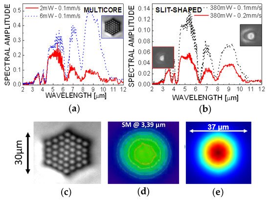
Further flexibility in the normalized frequency requires increasing even more the waveguide cross-section diameter, beyond the typical limit of the slit-shaping technique (tipically 10-15 µm). The flexibility in designing optical functions in a waveguide array concept is considerable, ranging from photonic crystal fibers to imaging devices, routers, and mode convertors [45][46][47]. In the context of LMA light transport, evanescently coupled fibers [48] or embedded waveguides [43] were demonstrated to be potential efficient solutions. The coupling efficiency in waveguide arrays is the key engineering factor in designing the properties of the array, and it can straightforwardly be designed using index contrast, inter-trace spacings, or lengths for various spectral domains. In terms of optical guiding, based on a multicore fiber concept, a matrix of waveguides permits upon central injection and gradual coupling in the next neighboring waveguides the development of in-phase modes that will coherently overlap, thus forming a large-area single mode covering the whole array. An example of photo-inscribed multicore array waveguides functioning in single-mode operation is given in Figure 2c. Typical hexagonal arrangements with 37 micron-spaced 10 mm-long traces were used in a Ge15As15S70 sample. For typical single trace NA below 0.05, equivalent to index contrasts of up to 5 × 10⁻⁴ at 800 nm, the individual modes superpose coherently and create super-single-mode propagation over the bundle cross-section. Higher NA and/or section diameters lead to stronger mode localization and favorable conditions for multimode guiding. The mode becomes more confined when increasing the index contrasts and keeping the diameter constant, or inversely can be extended with larger inter-trace separation and keeping the index contrast constant. Consequently, the single trace NA can be adjusted for single mode conditions, with losses around 1 dB/cm. Even larger sections (up to 100 µm or more) with multimode character can be obtained using multicore bundles with slit-shaped individual traces.
Tests of MIR light guiding with multicore and slit-shaped structures with index contrasts up or in excess of 10−3 are given in Figure 2. The results indicate high transmittance over the whole black body source range (2–13 µm) convoluted with the glass transparency window (0.5–11 µm) and the detector response (FLIR camera). The large band response in Figure 2a shows chromatic effects with apparent slightly higher attenuation at large wavelengths depending on the degree of mode confinement, obtained by increasing the waveguide index contrast. The chromaticity of the structures can be controlled via index contrast engineering. Chromatic effects are less apparent in slit-shaped traces (Figure 2b), with main index contrast effects in the overall guide transparency. Spatial mode profiles under coherent light injection were tested at 3.39 µm He-Ne laser radiations for multicore structures and show symmetric single mode guiding (Figure 2d) with mode areas matching the size of the multicore structure in Figure 2c. The result is confirmed by numerical simulations [9]. An example of a calculated mode is given in Figure 2e for a hexagonal structure having the same characteristic of the experimental one. The guiding performances were experimentally analyzed via the cut-back method on multicore guides of several lengths, indicating propagation losses in the 1 dB/cm range at 3.39 µm injection. More recently, Masselin et al. [49] showed that propagation losses as low as 0.11 dB/cm at 1.5 µm can be obtained by optimizing the index contrast of multicore structures in bulk ChGs. Other techniques and configurations have been proposed in the literature in order to increase the guiding cross-section area. These techniques are mainly based on depressed cladding concepts [16][50][51] (photo-inscription of a low index Type II cladding surrounding the guiding area), or on a 1D version of the multicore concept [52] (periodic arrangement of Type I index slabs). In particular, depressed-cladding techniques can be effective in bulk materials which cannot sustain contrasted Type I index structures, as is the case for example in As2S3 chalcogenide glass, as will be discussed below.

4. Signal Extraction by Embedded High-Aspect-Ratio Bessel Nanovoids
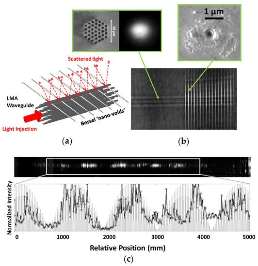
Reducing the size and power consumption of detecting instruments has always been an issue for spatial astronomical applications. Nowadays, with the development of Nanosat projects, the possibility of achieving very high resolution in a very compact and light device gives waveguide optics a very broad field of application. A possible approach is to develop integrated spectrometers where the spectrum is obtained by Fourier Transform of a static interferogram, as proposed in the SWIFTS-Lippmann configuration [53][54]. In the present approach, the stationary wave is obtained by superposing the direct and backward guided modes of a simple channel optical waveguide, the latter being obtained without using a mirror but only Fresnel reflection at the waveguide output, exploiting the high refractive index of GLS waveguides. For sampling the stationary wave inside the waveguide, periodic nanodots of gold sputtered on the surface [55], or grooves obtained by Focused Ion Beam technology (FIB) [54], are typically utilized. For the first time, the classical nano-scattering centers, fabricated by time-consuming lithographic techniques, are here replaced by Bessel high aspect-ratio nanovoids photo-written by DLW perpendicularly to the waveguide [10] (the energy scattered by the periodic nanostructure, which is then used to sample the signal transported in the waveguide), as shown in Figure 3a,b. Periodic Bessel nanovoids with a transverse section below 500 nm (see the inset on top-right of Figure 3b) and an axial dimension above 150 µm, separated by 10 µm were employed. As a guiding element, a photo-inscribed LMA waveguide was used, in order to achieve large diameter mode guiding in the NIR and MIR with single mode characteristics. This was based on a centered hexagonal arrangement of 37 parallel waveguides A view on the multicore waveguide cross-section structure and the corresponding guided mode at 1550 nm, with a diameter of about 20 µm, is shown in the top-left inset of Figure 3b. The trial was performed in GLS. The main interest of this technology is not only that the waveguide cross-section diameter and index can be adjusted in order to have single mode guiding at the desired wavelength, but also that the sampling nano-voids can be written in a very short time using DLW (few minutes) over the whole length of the sample (typically few cm, and this is highly suited in order to increase the spectral resolution), whereas classical techniques such as FIB or lithography take hours, and are limited to small lengths (typically 500 μm), requiring mask shifting in order to cover high areas. Moreover, the sampling nano-voids can be set at different depths in order to optimize interaction with the evanescent field of the waveguide, optimizing therefore the scattered signal, and finally their form factor can be easily changed, in order to modify the extraction efficiency and directivity [56]. This is a perfect demonstration of the high flexibility of the DLW technique in realizing compact embedded detectors, if compared to existing industrially mature lithographic techniques.

5. Photoinscription of 3D Nonlinear Optical Functions in Bulk ChG Glasses
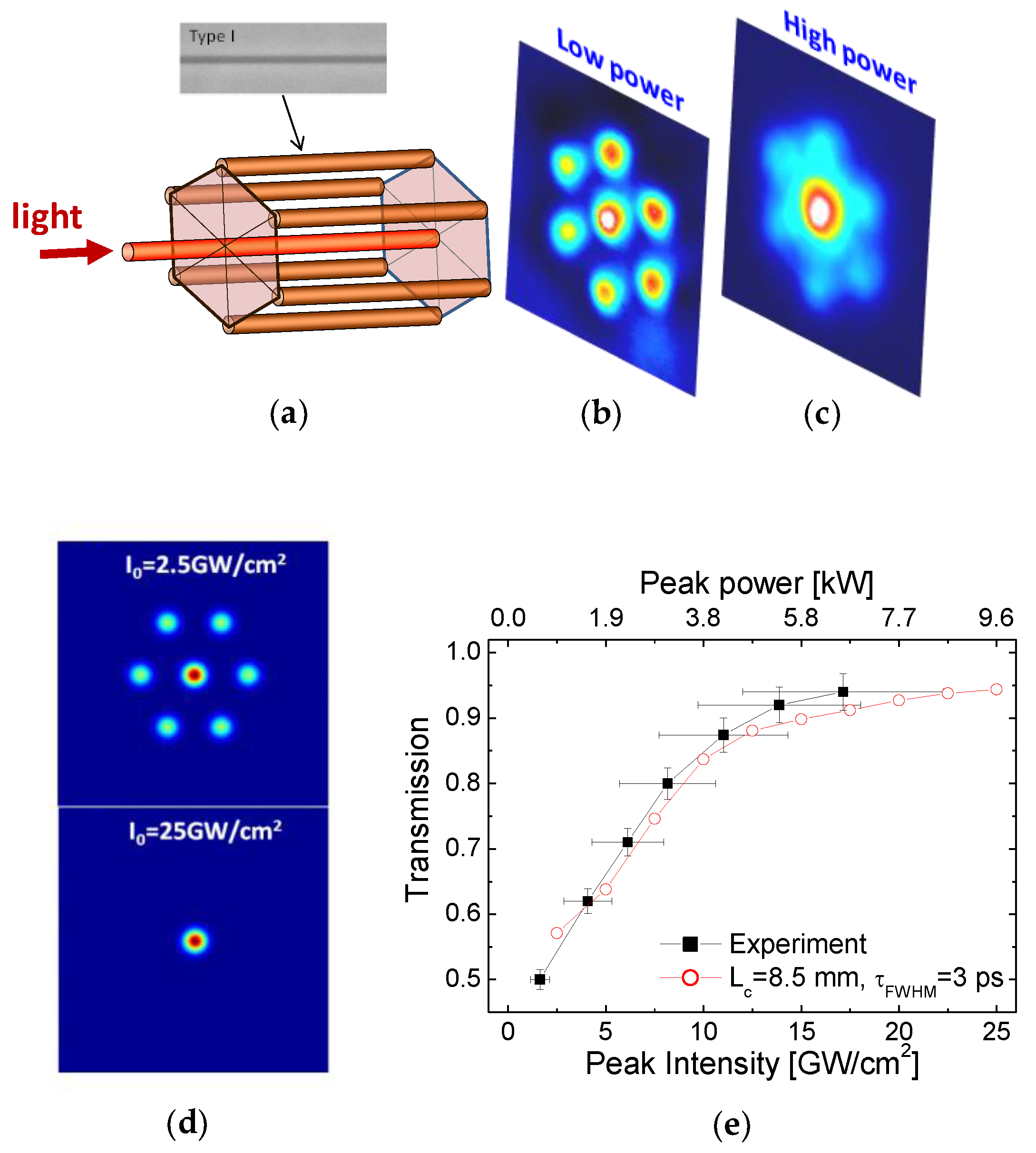
 Figure 4. (a) Conceptual design of the centered hexagonal array with a 9.1 mm length for the core guide and a 2.4 mm length for the surrounding hexagon. The inter-trace spacing is 13 μm; (b) Output mode in the case of low-power (0.2 kW) injection with a uniform spread of energy; (c) Output mode in the case of high-power (7 kW) injection with a core localization of light. The injected pulse duration (FWHM) is 3 ps; (d) Output mode snapshots resulting from the simulation of the propagation in the photonic saturable absorber of a λ = 800 nm positively chirped pulse of 3 ps, for an input pulse intensity of 2.5 GW/cm2 (top) and 25 GW/cm2 (bottom); (e) Intensity and power-dependent transmission in the hexagonal array. Experimental values (solid squares) and simulation data (open circles) are plotted. The x-error bars reflect the precision in evaluating the intensity via the accuracy of mode size estimations.
6. Conclusions
References
- Davis, K.M.; Miura, K.; Sugimoto, N.; Hirao, K. Writing waveguides in glass with a femtosecond laser. Opt. Lett. 1996, 21, 1729–1731.
- Itoh, K.; Watanabe, W.; Nolte, S.; Schaffer, C. Ultrafast processes for bulk modification of transparent materials. MRS Bull. 2006, 31, 620–625.
- Nolte, S.; Will, M.; Burghoff, J.; Tünnermann, A. Femtosecond waveguide writing: A new avenue to three-dimensional integrated optics. Appl. Phys. A Mater. Sci. Process. 2003, 77, 109–111.
- Pacchioni, G.; Skuja, L.; Griscom, D.L. Defects in SiO2 and Related Dielectrics: Science and Technology; Kluwer Academic Publishers: Dordrecht, The Netherlands, 2000.
- Mishchik, K.; D’Amico, C.; Velpula, P.K.; Mauclair, C.; Ouerdane, Y.; Boukenter, A.; Stoian, R. Ultrafast laser-induced electronic and structural modifications in bulk fused silica. J. Appl. Phys. 2013, 114, 133502.
- Masselin, P.; Le Coq, D.; Cuisset, A.; Bychkov, E. Spatially resolved Raman analysis of laser induced refractive index variation in chalcogenide glass. Opt. Mater. Express 2012, 2, 1768–1775.
- Cheng, G.; D’Amico, C.; Liu, X.; Stoian, R. Large mode area waveguides with polarization functions by volume ultrafast laser photoinscription of fused silica. Opt. Lett. 2013, 38, 1924–1926.
- Thomson, R.R.; Birks, T.A.; Leon-Saval, S.G.; Kar, A.K.; Bland-Hawthorn, J. Ultrafast laser inscription of an integrated photonic lantern. Opt. Express 2011, 19, 5698–5705.
- D’Amico, C.; Cheng, G.; Mauclair, C.; Troles, J.; Calvez, L.; Nazabal, V.; Caillaud, C.; Martin, G.; Arezki, B.; LeCoarer, E.; et al. Large-mode-area infrared guiding in ultrafast laser written waveguides in sulfur-based chalcogenide glasses. Opt. Express 2014, 22, 13091–14001.
- Martin, G.; Bhuyan, M.; Troles, J.; D’Amico, C.; Stoian, R.; Le Coarer, E. Near infrared spectro-interferometer using femtosecond laser written GLS embedded waveguides and nano-scatterers. Opt. Express 2017, 25, 8386–8397.
- Cvetojevic, N.; Jovanovic, N.; Gross, S.; Norris, B.; Spaleniak, I.; Schwab, C.; Withford, M.J.; Ireland, M.; Tuthill, P.; Guyon, O.; et al. Modal noise in an integrated photonic lantern fed diffraction-limited spectrograph. Opt. Express 2017, 25, 25546–25565.
- Watanabe, W.; Kuroda, D.; Itoh, K.; Nishii, J. Fabrication of Fresnel zone plate embedded in silica glass by femtosecond laser pulses. Opt. Express 2002, 10, 978–983.
- Monat, C.; Domachuk, P.; Eggleton, B.J. Integrated optofluidics: A new river of light. Nat. Photonics 2007, 1, 106–114.
- Marshall, G.D.; Dekker, P.; Ams, M.; Piper, J.A.; Withford, M.J. Directly written monolithic waveguide laser incorporating a distributed feedback waveguide-Bragg grating. Opt. Lett. 2008, 33, 956–958.
- Sansoni, L.; Sciarrino, F.; Vallone, G.; Mataloni, P.; Crespi, A.; Ramponi, R.; Osellame, R. Polarization Entangled State Measurement on a Chip. Phys. Rev. Lett. 2010, 105, 200503.
- Caulier, O.; LeCoq, D.; Bychkov, E.; Masselin, P. Direct laser writing of buried waveguide in As2S3 glass using a helical sample translation. Opt. Lett. 2013, 38, 4212–4215.
- Bland-Hawthorn, J.; Kern, P. Astrophotonics: A new era for astronomical instruments. Opt. Express 2009, 17, 1880–1884.
- Ta’eed, V.G.; Baker, N.J.; Fu, L.; Finsterbusch, K.; Lamont, M.R.E.; Moss, D.J.; Nguyen, H.C.; Eggleton, B.J.; Choi, D.Y.; Madden, S.; et al. Ultrafast all-optical chalcogenide glass photonic circuits. Opt. Express 2007, 15, 9205–9221.
- Thomson, R.R.; Kar, A.K.; Allington-Smith, J. Ultrafast laser inscription: An enabling technology for astrophotonics. Opt. Express 2009, 17, 1963–1969.
- Jovanovic, N.; Tuthill, P.G.; Norris, B.; Gross, S.; Stewart, P.; Charles, N.; Lacour, S.; Ams, M.; Lawrence, J.S.; Lehmann, A.; et al. Starlight demonstration of the Dragonfly instrument: An integrated photonic pupil-remapping interferometer for high-contrast imaging. Mon. Not. R. Astron. Soc. 2012, 427, 806–815.
- Cvetojevic, N.; Norris, B.R.M.; Gross, S.; Jovanovic, N.; Arriola, A.; Lacour, S.; Kotani, T.; Lawrence, J.S.; Withford, M.J.; Tuthill, P. Building hybridized 28-baseline pupil-remapping photonic interferometers for future high-resolution imaging. Appl. Opt. 2021, 60, D33–D42.
- Eggleton, B.; Luther-Davies, B.; Richardson, K. Chalcogenide photonics. Nat. Photonics 2011, 5, 141–148.
- Hu, J.; Meyer, J.; Richardson, K.; Shah, L. Feature issue introduction: Mid-IR photonic materials. Opt. Mater. Express 2013, 3, 1571–1575.
- Sanghera, J.S.; Aggarwal, I.D. Active and passive chalcogenide glass optical fibers for IR applications: A review. J. Non Cryst. Solids 2008, 256–257, 462–467.
- Gai, X.; Han, T.; Prasad, A.; Madden, S.; Choi, D.-Y.; Wang, R.; Bulla, D.; Luther-Davies, B. Progress in optical waveguides fabricated from chalcogenide glasses. Opt. Express 2010, 18, 26635–26646.
- Labadie, L.; Martin, G.; Anheier, N.C.; Arezki, B.; Qiao, H.A.; Bernacki, B.; Kern, P. First fringes with an integrated-optics beam combiner at 10µm. A new step towards instrument miniaturization for mid-infrared interferometry. Astron. Astrophys. 2011, 531, A48–A54.
- Vázquez, M.R.; Sotillo, B.; Rampini, S.; Bharadwaj, V.; Gholipour, B.; Fernández, P.; Ramponi, R.; Soci, C.; Eaton, S.M. Femtosecond laser inscription of nonlinear photonic circuits in Gallium Lanthanum Sulphide glass. J. Phys. Photonics 2019, 1, 015006.
- Kanbara, H.; Fujiwara, S.; Tanaka, K.; Nasu, H.; Hirao, K. Third-order nonlinear optical properties of chalcogenide glasses. Appl. Phys. Lett. 1997, 70, 925–927.
- Bindra, K.S.; Bookey, H.T.; Kar, A.K.; Wherrett, B.S.; Liu, X.; Jha, A. Nonlinear optical properties of chalcogenide glasses: Observation of multiphoton absorption. Appl. Phys. Lett. 2001, 9, 1939–1941.
- Zakery, A.; Elliott, S. Optical properties and applications of chalcogenide glasses: A review. J. Non Cryst. Solids 2003, 330, 1–12.
- Sanghera, J.S.; Florea, C.M.; Shaw, L.B.; Pureza, P.; Nguyen, V.Q.; Bashkansky, M.; Dutton, Z.; Aggarwal, I.D. Non-linear properties of chalcogenide glasses and fibers. J. Non Cryst. Solids 2008, 354, 462–467.
- Eggleton, B.J. Chalcogenide photonics: Fabrication, devices and applications Introduction. Opt. Express 2010, 18, 26632–26634.
- Hewak, D.W.; Brady, D.; Curry, R.J.; Elliott, G.; Huang, C.C.; Hughes, M.; Knight, K.; Mairaj, A.; Petrovich, M.N.; Simpson, R.E.; et al. Chalcogenide glasses for photonics device applications. In Photonic Glasses and Glass-Ceramics; Murugan, G.S., Ed.; Research Signpost: Thiruananthapuram, India, 2010; pp. 29–102.
- Hisakumi, H.; Tanaka, K. Giant photoexpansion in As2S3 glass. Appl. Phys. Lett. 1994, 65, 2925.
- Zarzycki, J. Glasses and the Vitreous State; Cambridge University Press: Cambridge, UK, 1991.
- Minardi, S.; Cheng, G.; D’Amico, C.; Stoian, R. Low-power-threshold photonic saturable absorber in nonlinear chalcogenide glass. Opt. Lett. 2015, 40, 257–259.
- Macedo, P.; Napolitano, A. Effects of a distribution of volume relaxation times in the annealing of BSC glass. J. Res. Natl. Bur. Stand. 1967, 71, 231–238.
- Calvez, L.; Yang, Z.; Lucas, P. Reversible giant photocontraction in chalcogenide glass. Opt. Express 2009, 17, 18581–18589.
- Gretzinger, T.; Fernandez, T.T.; Gross, S.; Arriola, A.; Withford, M.J. Boson band mapping: Revealing ultrafast laser induced structural modifications in chalcogenide glass. Opt. Lett. 2020, 45, 3369–3372.
- Lucas, P.; King, E.A. Calorimetric characterization of photoinduced relaxation in GeSe9 glass. J. Appl. Phys. 2006, 100, 023502.
- Caulier, O.; Le Coq, D.; Calvez, L.; Bychkov, E.; Masselin, P. Free carrier accumulation during direct laser writing in chalcogenide glass by light filamentation. Opt. Express 2011, 19, 20088–20096.
- Hisakumi, H.; Tanaka, K. Optical microfabrication of chalcogenide glasses. Science 1995, 270, 974–975.
- Boesch, L.; Napolitano, A.; Macedo, P.B. Spectrum of Volume Relaxation Times in B2O3. J. Am. Ceram. Soc. 1970, 53, 148–153.
- Cheng, Y.; Sugioka, K.; Midorikawa, K.; Masuda, M.; Toyoda, K.; Kawachi, M.; Shihoyama, K. Control of the cross-sectional shape of a hollow microchannel embedded in photo-structurable glass by use of a femtosecond laser. Opt. Lett. 2003, 28, 55–57.
- Osellame, R.; Taccheo, S.; Marangoni, M.; Ramponi, R.; Laporta, P.; Polli, D.; De Silvestri, S.; Cerullo, G. Femtosecond writing of active optical waveguides with astigmatically shaped beams. J. Opt. Soc. Am. B 2003, 20, 1559–1567.
- Keil, R.; Heinrich, M.; Dreisow, F.; Pertsch, T.; Tünnermann, A.; Nolte, S.; Christodoulides, D.N.; Szameit, A. All-optical routing and switching for three-dimensional photonic circuitry. Sci. Rep. 2011, 1, 94.
- Minardi, S.; Dreisow, F.; Grüfe, M.; Nolte, S.; Pertsch, T. Three-dimensional photonic component for multichannel coherence measurements. Opt. Lett. 2012, 37, 3030–3130.
- Crespi, A.; Osellame, R.; Ramponi, R.; Brod, D.J.; Galvao, E.F.; Spagnolo, N.; Vitelli, C.; Maiorino, E.; Mataloni, P.; Sciarrino, F. Integrated multimode interferometers with arbitrary designs for photonic boson sampling. Nat. Photonics 2013, 7, 545–549.
- Vogel, M.M.; Abdou-Ahmed, M.; Voss, A.; Graf, T. Very-large-mode-area single- mode multicore fiber. Opt. Lett. 2009, 34, 2876–2878.
- Masselin, P.; Bychkov, E.; Le Coq, D. Direct laser writing of a low-loss waveguide with independent control over the transverse dimension and the refractive index contrast between the core and the cladding. Opt. Lett. 2016, 41, 3507–3510.
- Long, X.; Bai, J.; Zhao, W.; Stoian, R.; Hui, R.; Cheng, G. Stressed waveguides with tubular depressed-cladding inscribed in phosphate glasses by femtosecond hollow laser beams. Opt. Lett. 2012, 37, 3138–3140.
- Tang, W.; Zhang, W.; Liu, X.; Liu, S.; Stoian, R.; Cheng, G. Tubular depressed cladding waveguide laser realized in Yb: YAG by direct inscription of femto- second laser. J. Opt. 2015, 17, 05803.
- Liu, X.; Zhang, W.; Zhao, W.; Stoian, R.; Cheng, G. Expanded-core waveguides written by femtosecond laser irradiation in bulk optical glasses. Opt. Express 2014, 22, 28771–28782.
- Le Coarer, E.; Blaize, S.; Benech, P.; Stefanon, I.; Morand, A.; L’erondel, G.; Leblond, G. Wavelength-scale stationary-wave integrated Fourier-transform spectrometry. Nat. Photonics 2007, 1, 473–478.
- Thomas, F.; Heidmann, S.; de Mengin, M.; Courjal, N.; Ulliac, G.; Morand, A.; Benech, P.; Le Coarer, E.; Martin, G. First Results in Near and Mid IR Lithium Niobate-Based Integrated Optics Interferometer Based on SWIFTS-Lippmann Concept. J. Light. Technol. 2014, 32, 4338–4344.
- Bonneville, C.; Thomas, F.; de Mengin Poirier, M.; LeCoarer, E.; Benech, P.; Gonthiez, T.; Morand, A.; Coutant, O.; Morino, E.; Puget, R.; et al. SWIFTS: A groundbreaking integrated technology for high performances spectroscopy and optical sensors. In Proceedings of the SPIE MOEMS Photonics West, San Francisco, CA, USA, 2–7 February 2013.
- Bonduelle, M.; Martin, G.; Perez, I.H.; Morand, A.; D’Amico, C.; Stoian, R.; Zhang, G.; Cheng, G. Laser written 3D 3T spectro-interferometer: Study and optimisation of the laser-written nano-antenna. In Proceedings of the SPIE 11446, Optical and Infrared Interferometry and Imaging VII, 114462T, online, CA, USA, 13 December 2020.
- Büttner, T.F.S.; Hudson, D.D.; Mägi, E.C.; Bedoya, A.C.; Taunay, T.; Eggleton, B.J. Multicore, tapered optical fiber for nonlinear pulse reshaping and saturable absorption. Opt. Lett. 2012, 37, 2469–2471.
- Bellec, M.; Panagiotopoulos, P.; Papazoglou, D.G.; Efremidis, N.K.; Couairon, A.; Tzortzakis, S. Observation and Optical Tailoring of Photonic Lattice Filaments. Phys. Rev. Lett. 2012, 109, 113905.
- Szameit, A.; Blömer, D.; Burghoff, J.; Schreiber, T.; Pertsch, T.; Nolte, S.; Tünnermann, A.; Lederer, F. Discrete nonlinear localization in femtosecond laser written waveguides in fused silica. Opt. Express 2005, 13, 10552–10557.
- Minardi, S.; Eilenberger, F.; Kartashov, Y.V.; Szameit, A.; Röpke, U.; Kobelke, J.; Schuster, K.; Bartelt, H.; Nolte, S.; Torner, L.; et al. Three-Dimensional Light Bullets in Arrays of Waveguides. Phys. Rev. Lett. 2010, 105, 263901.
- Hudson, D.D.; Shish, K.; Schibli, T.R.; Kutz, J.N.; Christodoulides, D.N.; Morandotti, R.; Cundiff, S.T. Nonlinear femtosecond pulse reshaping in waveguide arrays. Opt. Lett. 2008, 33, 1440–1442.
- Snyder, A.W. Coupled-Mode Theory for Optical Fibers. J. Opt. Soc. Am. 1972, 62, 1267–1277.
- Zhao, H.; Major, A. Powerful 67 fs Kerr-lens mode-locked prismless Yb:KGW oscillator. Opt. Express 2013, 21, 31846–31851.


