+1 credit
| Version | Summary | Created by | Modification | Content Size | Created at | Operation |
|---|---|---|---|---|---|---|
| 1 | Yong-Won Song | + 1992 word(s) | 1992 | 2021-04-07 11:20:21 |
Video Upload Options
Directly-Grown Graphene can be achieved through transfer-free graphene synthesis methods. Interfacial growth process enables the growth of a patterned graphene layer between the substrate and catalyst layers; it is a method conceived to avoid the transferring process by optimizing critical growth factors that affect the synthesis mechanism.
1. Introduction
In the recent past, silicon technology has dominated the electronic-to-data communication system of modern society. However, the industry is currently striving to meet the demand of faster and more efficient data processing, as the potential of silicon-based components seems to have reached a limit [1][2]. Accordingly, there have been recent discoveries in 2D materials and related studies to match the requirements of modern times. Hence, in the intense competition for the next dominant technology, graphene is considered to be a competent candidate.
Graphene is an exquisite 2D material comprising a one-atom-thick planar sheet of sp2-bonded carbon atoms. The structural configuration of graphene is a hexagonal honeycomb crystal that contains six carbon atoms. These atoms form strong σ-bonds and additional π–π* bonds by hybridization of the pz orbitals of the immediate carbon atoms in the hexagon. Graphene acts like a metal with a vanishing Fermi surface or a semiconductor having zero bandgap. This is due to its conduction and valance bands being symmetrical at the Dirac point where π–π and π*–π* overlap and result in a Fermi surface pin. The π electrons of graphene are compelled to have a low-energy band structure that resemble two symmetric cones representing valence and conduction bands that contact at the Dirac point at energies lower than 1 eV. Electron diffusion in this energy zone is known to be linear to a larger extent, akin to that of light, and unlike other conventional 2D materials with parabolic dispersion. The low-energy electronic arrangement is a spinor characteristic of graphene that regulates the inhibition of backscattering, which is a dominating factor for graphene with excellent transfer properties [3][4][5][6][7]. Nevertheless, graphene is an ideal photonic and optoelectronic material due to the broadband optical properties [8][9][10][11][12][13][14]. The aforementioned characteristics forge the path for graphene to be a potential material for optoelectronic and photonic applications [15][16][17][18][19][20][21][22][23][24][25][26][27][28][29][30].
Graphene synthesis was first accomplished by applying techniques such as micro- mechanical rift and epitaxial growth on SiC at elevated temperatures. For practical utilization, it is imperative to use synthesis methods that produce defect free, high quality graphene. Therefore, only limited approaches, such as mechanical exfoliation, carbon nanotube unzipping, epitaxial growth, self-assembly of surfactants, chemical vapor deposition (CVD), and chemical conversion, have been employed by researchers to synthesize graphene to meet the conditions of practical utilization [31][32][33][34][35][36][37][38]. Synthesis of monolayer graphene on a larger scale was achieved by large improvements to the CVD technique [39][40][41][42][43][44][45]. However, these approaches cannot ensure direct use of graphene in devices for many notable reasons, such as the use of metal catalysts, chemical etching of catalytic materials, transfer or exfoliation, complex chemical reactions, and high operational temperatures.
More importantly, it has been seen that optoelectronic and photonic devices are usually compact and not always planar; therefore, the transfer of 2D graphene synthesized by the prevailing methods onto practical non-planar, curvilinear, or customized substrates has critical limitations and disadvantages. Additionally, graphene is usually damaged under the mechanical and chemical stress of post-transfer treatment [46][47][48][49]. Therefore, a transfer-free, direct synthesis of graphene on arbitrary surfaces is highly anticipated for the development of optoelectronic and photonic devices. Furthermore, in the case of optoelectronic and photonic devices, it is not possible to exploit the efficient light-graphene interaction because 2D graphene cannot cover 3D devices in a conformal manner. Accordingly, an advanced study of graphene synthesis that promises to be more direct, less complex, cost-efficient, and readily applicable to 3D structures for device manufacturing is highly demanded, confirming the utilization of the potentials that graphene offers.
2. Application of Directly Grown Graphene
2.1. Ultrafast Fiber Laser
The excellent optical properties of graphene, such as its broadband saturable absorption, ultra-wide spectral range because of the straight scattering of Dirac electrons, unique energy band gap, and ultrafast recovery time, makes it suitable for ultrafast pulse generation and a powerful element for fiber lasers [50]. Several studies have proven that graphene can be an excellent SA for both mode-locking and Q-switching pulse generation in infrared wavelengths [51][52][53][54][55][56][57][58][59][60][61]. However, directly synthesized graphene contouring the surfaces of the 3D-structured optical devices is highly anticipated to maximize the nonlinear interaction with guided light. Here, we have discussed two processes, in situ and ACS, that enable growing graphene directly on the optical devices so that no further transferring is required. Accordingly, by providing maximum surface coverage and eliminating the interstices that frequently have been found for the suspended graphene cases, maximum light-matter interaction can be ensured [62].
A SA device, made of in situ grown graphene on the fiber end facet, as shown in Figure 1a, was employed to generate soliton pulses. The central wavelength and full width at half maximum (FWHM) of the generated ultrafast pulses were found to be λ = 1571.96 nm and 0.75 nm, respectively, as shown in Figure 1b. The pulse repetition rate was determined to be frep = 15.06 MHz with a pulse duration of 2.6 ns for sech2-profile as shown in Figure 1c. Later, as presented in Figure 1d, the in situ grown graphene on the polished surface of a D-shaped fiber device was employed in the same cavity to achieve femtosecond pulses. In this case, the generated pulse was centered at 1559 nm with a FWHM of 3.44 nm (see Figure 1e), where the pulse repetition rate was determined to be 8.93 MHz (see inset of Figure 1e); the generated pulse was found in the fs scale with a measured duration of 910 fs (see Figure 1f). The time-bandwidth product (TBP) value of 0.386, indicating the output pulses were slightly chirped, was calculated from the pulses. These results indicate the stability of the soliton pulses generated by in situ graphene.
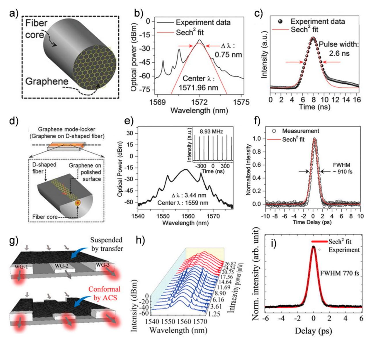
Figure 1. (a) Schematics of the mode-locker device made from in-situ grown graphene on SMF end facet; (b) Output characteristics of pulse spectrum in wavelength domain mode-locked with device shown in (a); (c) Pulse duration with the mode-locker device shown in (a); (d) Schematics of mode-locker device made from in-situ grown graphene on the flat face of a D-shaped fiber; (e) Output characteristics of pulse spectrum in wavelength domain mode-locked with device shown in (d); (f) Pulse duration with mode-locker device shown in (d); (g) Superiority of ACS-grown graphene over transferred graphene; (h) Intracavity power dependent optical spectra of the pulses; (d) Duration of the mode-locked pulses. (a–f) Reproduced with permission from [63]. Copyright WILEY-VCH Verlag GmbH & Co. KGaA, Weinheim, 2015. (g–i) Reproduced with permission from [62]. Copyright WILEY-VCH Verlag GmbH & Co. KGaA, Weinheim, 2020.
2.2. Ultrafast Optical Switching
In FWM, new frequency components can be generated either by using two strong pumps (ω1 ≠ ω2), which is called the non-degenerate case, or one strong pump (ω1 = ω2), which is called the degenerate case.
FWM is a nonlinear optical Kerr effect derivative that occurs if two waves propagate through a nonlinear medium simultaneously and generate one or two new waves. However, by attaching an optically nonlinear material to the polished surface of an optical fiber, the newly produced signal, based on the FWM concept, can be enhanced to enable ultrafast optical switching for ultra-high-speed optical communication systems. It has already been demonstrated by previous studies that various nonlinear 2D materials, such as carbon nanotubes and black phosphorus (BP) are suitable for FWM [64][65]. However, considering all the new features in the electronic and optical realms, such as nonlinear optical switching, FWM with graphene could be a new pathway for the computational design of systems and applications.
To investigate the FWM process with in situ grown graphene, two CW lasers were employed for the demonstration: one for launching the pump channel and another for the modulated signal channel (tunable) at λp = 1552.4 nm and λs = 1559 nm, respectively [66]. The resulting wavelengths of the newly produced optical channels were λChg1 = 1545 nm and λChg2 = 1566 nm for the aforementioned pump channel and signal channel (see Figure 2a), respectively. The in situ graphene-coated D-shaped fiber had a 2 dB (58.5% nonlinear increment) higher value of ER, as indicated in Figure 2b, than that of the bare D-shaped fiber.
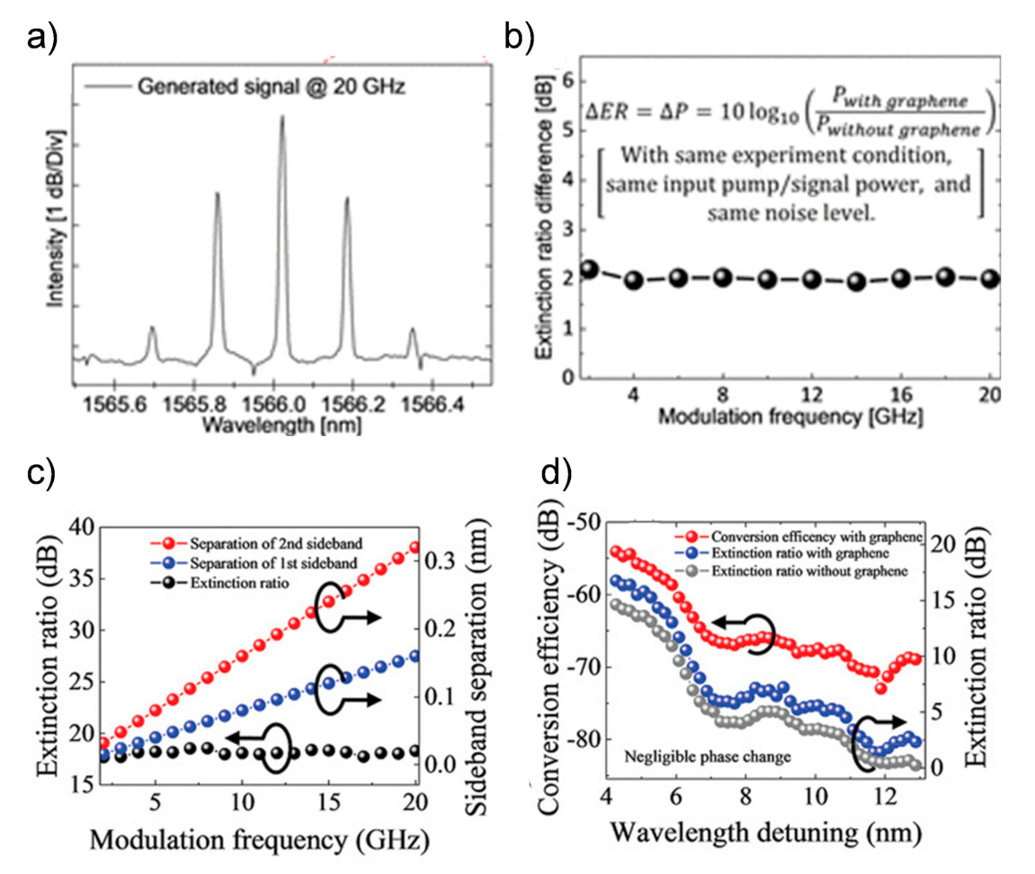
Figure 2. (a) Generated signal corresponding to original signal; (b) Extinction ratio (ER) comparison for without and with in-situ graphene cases; (c) Modulation frequency dependent sideband separation in FWM demonstration with ACS graphene; (d) Wavelength detuning dependent conversion efficiency (red curve) and ER (blue curve) for confirming negligible phase-mismatch during FWM experiment. (a,b) Reproduced with permission from [66]. Copyright American Chemical Society, 2018; (c,d) Reproduced with permission from [62]. Copyright WILEY-VCH Verlag GmbH & Co. KGaA, Weinheim, 2020.
2.3. Photodetection
A technique of explicit growth of graphene coatings on the surface of silicon nanoholes (SiNHs) through plasma enhanced chemical vapor deposition (PECVD) was projected to accomplish transfer-free conformal graphene/SiNH photo detectors for the first time [67]. The conformal graphene/SiNH structures were found to have an exceptional light absorption pursuance with absorptions risen up to 90%, and also consist high power absorption densities, that results in more photo carrier procreations per unit volume in the SiNHs than planar silicon. It was found that the photocurrent of the conformal graphene/SiNH photo detector is likely to be 34 μA, which is definitely much higher than the other fellows: planar graphene/Si (17 μA) and SiNHs (10 μA) as shown in Figure 3a. Consequently, the photo response speeds of three kinds of photo detectors, as shown in Figure 3b, were evaluated with respect to the light modulation frequencies at 1, 100, and 2500 Hz, and the results for the conformal graphene/SiNH photo detector were found to be satisfactory. For all switching frequencies, the photo detectors can switch swiftly between “on” and “off” states. Hence, the conformal graphene/SiNH photo detectors are quicker than the other two detectors because the carriers originated in SiNHs can infuse into the nearby conformal graphene more promptly. These consequences emerge from the lower reflections, higher absorption densities, and shorter carrier transport paths in conformal graphene/SiNH detectors.
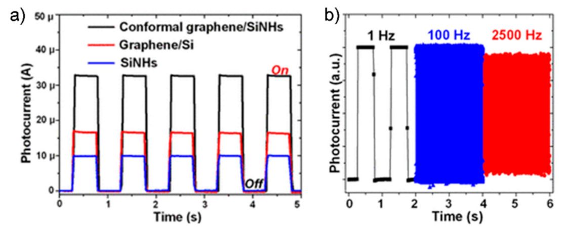
Figure 3. (a) Photoresponse of the graphene/Si, SiNHs, and conformal graphene/SiNH photodetectors; (b) Photoresponse of the proposed photodetectors at 1, 100, and 2500 Hz of frequencies. (a), (b) Reproduced with permission from [67]. Copyright American Chemical Society, 2019.
3. Conclusions
In addition to the superior coverage of graphene by the direct method, conformal growth is a great benefit that nullifies interstices frequently observed in suspended graphene cases. Nevertheless, the distance (distance from catalyst to the target substrates) functional growth of graphene exhibits tunable semiconducting properties that can be exploited for nanoelectronic devices. Demonstrations of ultrafast optical pulses in both Q-switching and mode-locking domains with in-situ and ACS grown graphene-enabled devices were possible. Ultrafast optical switching up to 20 GHz modulation frequency has been demonstrated by graphene grown in situ, and ACS methods indicate that the optical nonlinearity is sufficiently high. In addition to their excellent electronic and optical properties, these direct growth methods strengthen the candidacy of graphene for optoelectronic and photonic devices. The verified optical nonlinearity with direct growth methods on fiber devices can pave the way for implementation in futuristic graphene-enabled hybrid optoelectronic and photonic devices.
The in situ and ACS methods, evidently different from other conventional methods, can develop transfer-free, directly synthesized graphene on optical devices. Furthermore, the ACS method has exhibited potential as a practical solution for direct synthesis of graphene on arbitrary 3D substrates. This method is a breakthrough for future on-chip optical signal processing and optical interconnects along with the chip-scale integration of electro-optic hybrid devices. In recent studies, the possibility of graphene-based integrated devices has been analyzed. Thus, graphene can also be used in broad-ranging optical control schemes. Therefore, the fabrication of silicon-based integrated optical circuits, which are expected to be used in numerous operations, such as pulsed light generation, routing, modulation, computing, and detection, can be enabled. Moreover, the integration of graphene into hybrid silicon photonics could be possible by direct deposition of graphene onto silicon. Therefore, graphene research may spawn a technological revolution that could possibly turn into a paradigm shift for ultrafast optics.
References
- Waldrop, M.M. The chips are down for Moore’s law. Nat. Cell Biol. 2016, 530, 144–147.
- Schulz, M. The end of the road for silicon? Nat. Cell Biol. 1999, 399, 729–730.
- Neto, A.C.; Guinea, F.; Peres, N.M.; Novoselov, K.S.; Geim, A.K. The electronic properties of graphene. Rev. Mod. Phys. 2009, 81, 109.
- Allen, M.J.; Tung, V.C.; Kaner, R.B. Honeycomb Carbon: A Review of Graphene. Chem. Rev. 2010, 110, 132–145.
- Avouris, P. Graphene: Electronic and Photonic Properties and Devices. Nano Lett. 2010, 10, 4285–4294.
- Geim, A.K.; Novoselov, K.S. The rise of graphene. Nat. Mater. 2007, 6, 183–191.
- Das Sarma, S.; Adam, S.; Hwang, E.H.; Rossi, E. Electronic transport in two-dimensional graphene. Rev. Mod. Phys. 2011, 83, 407–470.
- Nair, R.R.; Blake, P.; Grigorenko, A.N.; Novoselov, K.S.; Booth, T.J.; Stauber, T.; Peres, N.M.R.; Geim, A.K. Fine Structure Constant Defines Visual Transparency of Graphene. Science 2008, 320, 1308.
- Hasan, T.; Sun, Z.; Wang, F.; Bonaccorso, F.; Tan, P.H.; Rozhin, A.G.; Ferrari, A.C. Nanotube–polymer composites for ultrafast photonics. Adv. Mater. 2009, 21, 3874–3899.
- Yamashita, S. A Tutorial on Nonlinear Photonic Applications of Carbon Nanotube and Graphene. J. Light. Technol. 2011, 30, 427–447.
- Lui, C.H.; Mak, K.F.; Shan, J.; Heinz, T.F. Ultrafast Photoluminescence from Graphene. Phys. Rev. Lett. 2010, 105, 127404.
- Wu, Y.; Wang, B.; Ma, Y.; Huang, Y.; Li, N.; Zhang, F.; Chen, Y. Efficient and large-scale synthesis of few-layered graphene using an arc-discharge method and conductivity studies of the resulting films. Nano Res. 2010, 3, 661–669.
- Hendry, E.; Hale, P.J.; Moger, J.J.; Savchenko, A.K.; Mikhailov, S.A. Coherent Nonlinear Optical Response of Graphene. Phys. Rev. Lett. 2010, 105, 097401.
- Zhang, H.; Virally, S.; Bao, Q.; Ping, L.K.; Massar, S.; Godbout, N.; Kockaert, P. Z-scan measurement of the nonlinear refractive index of graphene. Opt. Lett. 2012, 37, 1856–1858.
- Han, M.Y.; Oezyilmaz, B.; Zhang, Y.; Kim, P. Energy Band-Gap Engineering of Graphene Nanoribbons. Phys. Rev. Lett. 2007, 98, 206805.
- Lemme, M.C.; Echtermeyer, T.J.; Baus, M.; Kurz, H. A Graphene Field-Effect Device. IEEE Electron Device Lett. 2007, 28, 282–284.
- Lin, Y.-M.; Dimitrakopoulos, C.; Jenkins, K.A.; Farmer, D.B.; Chiu, H.-Y.; Grill, A.; Avouris, P. 100-GHz transistors from wafer-scale epitaxial graphene. Science 2010, 327, 662.
- Lee, S.; Kim, J.T.; Song, Y.-W. Graphene-Incorporated Soft Capacitors for Mechanically Adjustable Electro-Optic Modulators. ACS Appl. Mater. Interfaces 2018, 10, 40781–40788.
- Lee, S.; Song, Y.-W. Graphene Self-Phase-Lockers Formed around a Cu Wire Hub for Ring Resonators Incorporated into 57.8 Gigahertz Fiber Pulsed Lasers. ACS Nano 2020, 14, 15944–15952.
- Ryu, B.; Kim, J.T.; Song, Y.-W. Graphene-dispersed polymer waveguide for efficient formation of mode-locked lasers at extremely low graphene concentration. Carbon 2020, 166, 123–130.
- Ryu, B.; Lee, S.; Kim, J.T.; Song, Y.-W. Efficient Optical Saturable Absorbers with Graphene on Polymer Waveguides for Femtosecond Laser Pulse Formation. Ann. Phys. 2018, 530.
- Kovalchuk, O.; Uddin, S.; Lee, S.; Song, Y.-W. Graphene Capacitor-Based Electrical Switching of Mode-Locking in All-Fiberized Femtosecond Lasers. ACS Appl. Mater. Interfaces 2020, 12, 54005–54011.
- Bao, Q.; Zhang, H.; Yang, J.-X.; Wang, S.; Tang, D.Y.; Jose, R.; Ramakrishna, S.; Lim, C.T.; Loh, K.P. Graphene-Polymer Nanofiber Membrane for Ultrafast Photonics. Adv. Funct. Mater. 2010, 20, 782–791.
- Zheng, Z.; Zhao, C.; Lu, S.; Chen, Y.; Li, Y.; Zhang, H.; Wen, S. Microwave and optical saturable absorption in graphene. Opt. Express 2012, 20, 23201–23214.
- Liu, M.; Yin, X.; Ulin-Avila, E.; Geng, B.; Zentgraf, T.; Ju, L.; Wang, F.; Zhang, X. A graphene-based broadband optical modulator. Nat. Cell Biol. 2011, 474, 64–67.
- Gao, Y.; Shiue, R.-J.; Gan, X.; Li, L.; Peng, C.; Meric, I.; Wang, L.; Szep, A.; Walker, D.; Hone, J.; et al. High-Speed Electro-Optic Modulator Integrated with Graphene-Boron Nitride Heterostructure and Photonic Crystal Nanocavity. Nano Lett. 2015, 15, 2001–2005.
- Tong, S.W.; Wang, Y.; Zheng, Y.; Ng, M.-F.; Loh, K.P. Graphene Intermediate Layer in Tandem Organic Photovoltaic Cells. Adv. Funct. Mater. 2011, 21, 4430–4435.
- Wu, J.; Agrawal, M.; Becerril, H.A.; Bao, Z.; Liu, Z.; Chen, Y.; Peumans, P. Organic Light-Emitting Diodes on Solution-Processed Graphene Transparent Electrodes. ACS Nano 2009, 4, 43–48.
- Xia, F.; Mueller, T.; Golizadeh-Mojarad, R.; Freitag, M.; Lin, Y.-M.; Tsang, J.; Perebeinos, V.; Avouris, P. Photocurrent Imaging and Efficient Photon Detection in a Graphene Transistor. Nano Lett. 2009, 9, 1039–1044.
- Mueller, T.; Xia, F.; Avouris, P. Graphene photodetectors for high-speed optical communications. Nat. Photon 2010, 4, 297–301.
- Kim, W.S.; Moon, S.Y.; Park, N.-H.; Huh, H.; Shim, K.B.; Ham, H. Electrical and Structural Feature of Monolayer Graphene Produced by Pulse Current Unzipping and Microwave Exfoliation of Carbon Nanotubes. Chem. Mater. 2011, 23, 940–944.
- Li, N.; Wang, Z.; Zhao, K.; Shi, Z.; Gu, Z.; Xu, S. Large scale synthesis of N-doped multi-layered graphene sheets by simple arc-discharge method. Carbon 2010, 48, 255–259.
- Pang, S.; Englert, J.M.; Tsao, H.N.; Hernandez, Y.; Hirsch, A.; Feng, X.; Müllen, K. Extrinsic Corrugation-Assisted Mechanical Exfoliation of Monolayer Graphene. Adv. Mater. 2010, 22, 5374–5377.
- Poon, S.W.; Chen, W.; Tok, E.S.; Wee, A.T.S. Probing epitaxial growth of graphene on silicon carbide by metal decoration. Appl. Phys. Lett. 2008, 92, 104102.
- Shen, B.; Ding, J.; Yan, X.; Feng, W.; Li, J.; Xue, Q. Influence of different buffer gases on synthesis of few-layered graphene by arc discharge method. Appl. Surf. Sci. 2012, 258, 4523–4531.
- Sinitskii, A.; Fursina, A.A.; Kosynkin, D.V.; Higginbotham, A.L.; Natelson, D.; Tour, J.M. Electronic transport in monolayer graphene nanoribbons produced by chemical unzipping of carbon nanotubes. Appl. Phys. Lett. 2009, 95, 253108.
- Suk, J.W.; Lee, W.H.; Kang, T.J.; Piner, R.D.; Won, S.J.; Hyoung, L.W.; June, K.T. Transfer of Chemical Vapor Deposition-Grown Monolayer Graphene by Alkane Hydrocarbon. Sci. Adv. Mater. 2016, 8, 144–147.
- Tan, H.; Fan, Y.; Rong, Y.; Porter, B.; Lau, C.S.; Zhou, Y.; He, Z.; Wang, S.; Bhaskaran, H.; Warner, J.H. Doping Graphene Transistors Using Vertical Stacked Monolayer WS2 Heterostructures Grown by Chemical Vapor Deposition. ACS Appl. Mater. Interfaces 2016, 8, 1644–1652.
- Bae, S.; Kim, H.K.; Lee, Y.; Xu, X.; Park, J.-S.; Zheng, Y.; Balakrishnan, J.; Lei, T.; Kim, H.R.; Song, Y.I.; et al. Roll-to-roll production of 30-inch graphene films for transparent electrodes. Nat. Nanotechnol. 2010, 5, 574–578.
- Kim, K.S.; Zhao, Y.; Jang, H.; Lee, S.Y.; Kim, J.M.; Kim, K.S.; Ahn, J.-H.; Kim, P.; Choi, J.-Y.; Hong, B.H. Large-scale pattern growth of graphene films for stretchable transparent electrodes. Nature 2009, 457, 706–710.
- Lee, S.; Lee, K.; Zhong, Z. Wafer Scale Homogeneous Bilayer Graphene Films by Chemical Vapor Deposition. Nano Lett. 2010, 10, 4702–4707.
- Li, X.; Cai, W.; An, J.; Kim, S.; Nah, J.; Yang, D.; Piner, R.; Velamakanni, A.; Jung, I.; Tutuc, E.; et al. Large-Area Synthesis of High-Quality and Uniform Graphene Films on Copper Foils. Science 2009, 324, 1312–1314.
- Reina, A.; Jia, X.; Ho, J.; Nezich, D.; Son, H.; Bulovic, V.; Dresselhaus, M.S.; Kong, J. Large Area, Few-Layer Graphene Films on Arbitrary Substrates by Chemical Vapor Deposition. Nano Lett. 2009, 9, 30–35.
- Sun, Z.; Yan, Z.; Yao, J.; Beitler, E.; Zhu, Y.; Tour, J.M. Growth of graphene from solid carbon sources. Nat. Cell Biol. 2010, 468, 549–552.
- Yan, K.; Peng, H.; Zhou, Y.; Li, H.; Liu, Z. Formation of Bilayer Bernal Graphene: Layer-by-Layer Epitaxy via Chemical Vapor Deposition. Nano Lett. 2011, 11, 1106–1110.
- Su, C.-Y.; Lu, A.-Y.; Xu, Y.; Chen, F.-R.; Khlobystov, A.N.; Li, L.-J. High-Quality Thin Graphene Films from Fast Electrochemical Exfoliation. ACS Nano 2011, 5, 2332–2339.
- Ishigami, M.; Chen, J.H.; Cullen, W.G.; Fuhrer, M.S.; Williams, E.D. Atomic Structure of Graphene on SiO2. Nano Lett. 2007, 7, 1643–1648.
- Pirkle, A.; Chan, J.; Venugopal, A.; Hinojos, D.; Magnuson, C.W.; McDonnell, S.; Colombo, L.; Vogel, E.M.; Ruoff, R.S.; Wallace, R.M. The effect of chemical residues on the physical and electrical properties of chemical vapor deposited graphene transferred to SiO2. Appl. Phys. Lett. 2011, 99, 122108.
- Suk, J.W.; Kitt, A.; Magnuson, C.W.; Hao, Y.; Ahmed, S.; An, J.; Swan, A.K.; Goldberg, B.B.; Ruoff, R.S. Transfer of CVD-Grown Monolayer Graphene onto Arbitrary Substrates. ACS Nano 2011, 5, 6916–6924.
- Bonaccorso, F.; Sun, Z.; Hasan, T.; Ferrari, A.C. Graphene photonics and optoelectronics. Nat. Photon 2010, 4, 611–622.
- Sun, Z.; Hasan, T.; Torrisi, F.; Popa, D.; Privitera, G.; Wang, F.; Bonaccorso, F.; Basko, D.M.; Ferrari, A.C. Graphene Mode-Locked Ultrafast Laser. ACS Nano 2010, 4, 803–810.
- Bao, Q.; Zhang, H.; Wang, Y.; Ni, Z.; Yan, Y.; Shen, Z.X.; Loh, K.P.; Tang, D.Y. Atomic-Layer Graphene as a Saturable Absorber for Ultrafast Pulsed Lasers. Adv. Funct. Mater. 2009, 19, 3077–3083.
- Song, Y.-W.; Jang, S.-Y.; Han, W.-S.; Bae, M.-K. Graphene mode-lockers for fiber lasers functioned with evanescent field interaction. Appl. Phys. Lett. 2010, 96, 051122.
- Chang, Y.M.; Kim, H.; Lee, J.H.; Song, Y.-W. Multilayered graphene efficiently formed by mechanical exfoliation for nonlinear saturable absorbers in fiber mode-locked lasers. Appl. Phys. Lett. 2010, 97, 211102.
- Popa, D.; Sun, Z.; Hasan, T.; Torrisi, F.; Wang, F.; Ferrari, A.C. Graphene Q-switched, tunable fiber laser. Appl. Phys. Lett. 2011, 98, 073106.
- Zhang, H.; Tang, D.; Knize, R.J.; Zhao, L.; Bao, Q.; Loh, K.P. Graphene mode locked, wavelength-tunable, dissipative soliton fiber laser. Appl. Phys. Lett. 2010, 96, 111112.
- Zhang, H.; Tang, D.Y.; Zhao, L.M.; Bao, Q.L.; Loh, K.P. Large energy mode locking of an erbium-doped fiber laser with atomic layer graphene. Opt. Express 2009, 17, 17630–17635.
- Zhang, H.; Tang, D.; Zhao, L.; Bao, Q.; Loh, K.P. Vector dissipative solitons in graphene mode locked fiber lasers. Opt. Commun. 2010, 283, 3334–3338.
- Martinez, A.; Fuse, K.; Yamashita, S. Mechanical exfoliation of graphene for the passive mode-locking of fiber lasers. Appl. Phys. Lett. 2011, 99, 121107.
- Zhao, L.M.; Tang, D.Y.; Zhang, H.; Wu, X.; Bao, Q.; Loh, K.P. Dissipative soliton operation of an ytterbium-doped fiber laser mode locked with atomic multilayer graphene. Opt. Lett. 2010, 35, 3622–3624.
- Bao, Q.; Zhang, H.; Ni, Z.; Wang, Y.; Polavarapu, L.; Shen, Z.; Xu, Q.-H.; Tang, D.; Loh, K.P. Monolayer graphene as a saturable absorber in a mode-locked laser. Nano Res. 2011, 4, 297–307.
- Uddin, S.; Song, Y.W. Atomic Carbon Spraying: Direct Growth of Graphene on Customized 3D Surfaces of Ultrafast Optical Devices. Adv. Opt. Mater. 2020, 8, 1902091.
- Debnath, P.C.; Park, J.; Scott, A.M.; Lee, J.; Lee, J.H.; Song, Y.-W. In Situ Synthesis of Graphene with Telecommunication Lasers for Nonlinear Optical Devices. Adv. Opt. Mater. 2015, 3, 1264–1272.
- Chow, K.K.; Yamashita, S. Four-wave mixing in a single-walled carbon-nanotube-deposited D-shaped fiber and its application in tunable wavelength conversion. Opt. Express 2009, 17, 15608–15613.
- Uddin, S.; Debnath, P.C.; Park, K.; Song, Y.-W. Nonlinear Black Phosphorus for Ultrafast Optical Switching. Sci. Rep. 2017, 7, srep43371.
- Debnath, P.C.; Uddin, S.; Song, Y.-W. Ultrafast All-Optical Switching Incorporatingin SituGraphene Grown along an Optical Fiber by the Evanescent Field of a Laser. ACS Photon 2017, 5, 445–455.
- Yang, J.; Tang, L.L.; Luo, W.; Shen, J.; Zhou, D.H.; Feng, S.L.; Wei, X.Z.; Shi, H.F. Light Trapping in Conformal Graphene/Silicon Nanoholes for High-Performance Photodetectors. ACS Appl. Mater. Inter. 2019, 11, 30421–30429.