+1 credit
| Version | Summary | Created by | Modification | Content Size | Created at | Operation |
|---|---|---|---|---|---|---|
| 1 | Labonnah Rahman | + 3091 word(s) | 3091 | 2021-03-29 10:03:23 | | | |
| 2 | Lily Guo | Meta information modification | 3091 | 2021-04-08 05:35:49 | | |
Video Upload Options
CP design topologies have been analyzed with different design and process schemes in the last decades .
1. Introduction
In the last decade, CP design topologies have been analyzed with different design and process schemes. In this literature, some of the principal structures of CP circuits have been presented, based on the basic design methods of Dickson and Cockcroft and Walton’s CP circuit. The increment in power supply voltage can achieve by voltage multiplication and integrating an additional one diode-capacitor voltage stage in series. In this study, different topologies, which have evolved in the last couple of years, have been discussed based on their applicability in other applications with the comparative analysis. Thus, different design schemes are classified as compatibility in-memory application, DC–DC converters and energy harvesting purposes.
2. Basic CP Circuits
Cockcroft and Walton (1932), at the Cavendish Laboratory in Cambridge, England, needed higher particle energies to accelerate sub-atomic particles along a straight discharge tube. A voltage multiplier circuit designed using a stack of capacitors connected to diodes acting as switches. By asserting and de-asserting the switches in proper sequence, they built up a potential of 800 kV [1]. This voltage multiplier circuit was far lighter and cheaper than transformers. Cockroft and Walton designed a voltage multiplier, which converted low AC power or DC pulses to a higher DC voltage level as shown in Figure 1. In this design, capacitors were connected in series, where diodes were employed to produce high voltage.
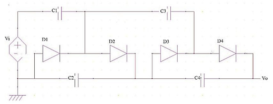
Figure 1. Schematic diagram of Cockcroft–Walton voltage multiplier [1].
Moreover, this scheme eliminated the heavy core as transformers did. In this method, the bulk of insulation/potting is required. A higher voltage was achieved from a low supply voltage using these capacitors and diodes as a multiplier. It had the advantage of low-cost materials requirement with an easy setup method [2]. However, this scheme suffered from some drawbacks; if the number of stages increased, then the higher stage’s voltage started to “sag” due to capacitors’ electrical impedance and the small number of steps. Moreover, when the output current is injected, a large voltage ripple is produced to increment the stages.
Dickson (1976) used the same concept as the Cockcroft–Walton voltage multiplication circuit and implemented it in IC’s. It was very similar to the CP voltage multiplier, where the diode-connected chains are coupled to the input through several capacitors connected in parallel. Therefore, all the capacitors needed to withstand storing the full voltages produced by these chains. The system could achieve efficient multiplication by involving many capacitors. However, involving many capacitors in the circuitry increased the power dissipation and decreased pumping efficiency [3]. The primary Dickson CP circuit was very robust with different high voltage generation issues until sub-micron design technology. When the diode-connected MOSFET was turned on in the Dickson CP circuit, the threshold voltage was the voltage difference between the drain and source terminal of the diode-connected MOSFET. The conventional Dickson CP circuit structure had a low pumping capacity due to the large threshold voltage and the body-effect in each stage to generate the high voltages as shown in Figure 2. Additionally, all the steps suffered from a high-voltage overstress and a voltage difference, which was 2xVDD in each node caused by each node’s gate oxides. Consequently, when the number of pumping stages increases, the body effect degrades the Dickson CP circuit’s pumping efficiency.
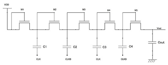
Figure 2. Dickson charge pump (CP) circuit with diode-capacitor [3].
Dickson CP circuit could not generate the desired output voltage as it was suffering from the body effect on the diode-connected MOSFETs. Therefore, Witters et al. (1989) proposed a new mechanism for designing a triple-well process CP [4]. In complementary metal-oxide-semiconductor (CMOS) circuit design, voltage multiplier circuits used a transistor, which performed as diodes. However, threshold voltage arises to the transistor in this circuit’s chain due to the body effect problem the performance affected slightly. The output voltage level could not meet the requirements compared to a diode configuration, which eventually reduced the circuit’s internal resistance. This difference between these methods got worse when any circuit implementation required more stages. Any multiplier or boosting circuit’s output voltage was limited, regardless of the necessary number of steps.
Moreover, the substrate current produced in the floating-well technique affects other circuits in the same chip. Therefore, this scheme for multiplying circuit was proposed and verified for implementation. Nevertheless, this technique predicted the characteristics of a wide variety of voltage multipliers.
Atsumi et al. (1994) designed a striking and widely-implemented CP circuit named bootstrap CP. In this scheme, a simple MOS transistor or transmission gate have utilized as a switching terminal to generate higher voltage than the power supply voltage. Therefore, the MOS transistor has to switch on with a suitable supply voltage to the gate terminal, higher than the source terminal voltage. These required high gate voltages were attained from each stage to another capacitor and MOS transistor, forming the bootstrap circuit. Though the circuit generated higher output voltage, it is also clear from the complex circuit structure that it required higher implementation cost for a more complex clocking scheme and control section, which has four phases and double amplitude of the supply voltage [5][6].
3. CP for Memory Application
Lauterbach et al. (2000) illustrated a novel idea of power saving in boosted CP circuits, which doubles the power efficiency by integrating two-step adiabatic switching, charge sharing, and a simplified clocking arrangement. As this scheme shares the charges, so clock driver strengths declined. Therefore, the maximum value of the charging current dropped by a factor of three. On the other hand, combining the tri-state drivers and the clocking circuits removed the parasitic charge current peaks. As a result, the electromagnetic emission of the CP circuit condensed considerably. However, the charge-sharing concept necessitates this external clock generator to pump the voltage, ultimately increasing power dissipation [7].
Lai and Wang (2001) proposed a CP circuit where source-bulk-connected techniques were utilized with two associated courses, which solved the limitation of charge sharing methods. These circuits are involved in the primary CP circuit to reduce the body effect while avoiding the forward-biased PN junction. The body of each charge transfer transistor in the primary pumping circuit is connected to the body bias circuit. When pumping begins, the CP circuit draws the current from CL and the internal node voltage becomes lower. However, in the source-bulk connected techniques, the large bulk-to-well PN-junction capacitance increased the parasitic capacitance at each pumping node. Second, to control the diode-connected MOSFETs’ body terminals dynamically, auxiliary MOSFETs are used in the source-bulk scheme, which generated the substrate current floating-well devices. However, using these extra circuitries caused large power dissipation with a large chip area [8].
Tanzawa et al. (2002) proposed a CP based on Umezawa et al.’s design principle. The proposed CP configuration required several logic circuits and PC2 switches. In this design, an additional circuit is added, which reduces the number of PC1 elements to only four. Moreover, most of the capacitors in the PC1 scheme only added a 10% increment of the total area in the PC2 method. Additionally, in this design, only high voltage transistors are included with intrinsic capacitors [9].
Pelliconi et al. (2003) proposed a power-efficient charge pump in 2003, including low-voltage transistors and a simple two-phase clocking scheme. In this method, higher operating clocks have engaged compared to other conventional methods. As a result, it has obtained high-current, high-efficiency and small-chip area. Around 100 MHz clock frequency has been received from the measured results. However, the circuit has secured fast switching times on low resistance and low capacitors. However, the circuit could not manage higher efficiency and boosted output voltage [10].
In 2005, Yan and Min proposed a CP method based on all P-channel metal–oxide–semiconductor (PMOS) transistors, suitable for the standard CMOS process. In this scheme, only low voltage PMOS transistors are used with the switching substrate technique to boost the transistors. Moreover, in this design, body effects have been eliminated to increase the output voltage and threshold voltage loss. This body effect was also reduced by employing the linear operation of PMOS based charge transfer switches. Therefore, this scheme has become compatible with low voltage memory applications. However, using all the PMOS transistors for transferring charge from one stage to another substrate current increased, resulting in higher power dissipation [11].
In 2008, Su and Ma proposed a four-phase CP circuit to reduce the reversion and conduction loss in each step. In this scheme, the voltage drop method is reduced in each sub-cell during the power stage. As a result, higher efficiency has been achieved with a low ripple and lower fabrication cost. Moreover, involving a subthreshold clock generator reduced the power loss in the controller. Therefore, it has provided an effective solution to the applications related to low voltage and low-power system-on-chip power converters. However, due to many capacitors, the proposed CP is not entirely free from parasitic effects [12].
Richelli et al. presented two CP methods for NVM with dynamic biasing of the gate and the body voltages. In this scheme, the device voltage loss problem created due to the device threshold has been controlled through gate and body biasing of every pass transistor. By using this scheme, a charge was pumped with minimal voltage drop and high conductivity. This scheme provided higher output voltage and pumping efficiency with involving only a two-phase clocking scheme. However, this design occupied a large chip area due to two pumping stages [13][14][15].
4. CP for DC–DC Converter
Shiau et al. (2007) implemented a polysilicon diode-based low voltage CP. There is no limitation of the boosted output voltage in this scheme, as polysilicon diodes are fully isolated from the silicon substrate as shown in Figure 3. Moreover, in this design method, CP is not limited by MOSFETs junction breakdown voltage, which can implement in a standard CMOS process. However, in this scheme, the body effect has not been eliminated, which is the main disadvantage of a diode-based CP circuit [16].
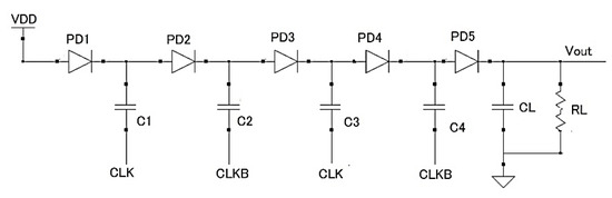
Figure 3. Static charge transfers switch based CP circuit [16].
Huang et al. proposed a CP circuit based on dual-phase mode [17]. In this scheme, several phases have been observed with the completely compact CP circuit with multiphase current-mode control. This structure involved the sensor stage, the buffer stage, the power stage, the automatic body switching (ABS) circuit, and the non-overlap circuit. The proposed structure claimed to have low ripple voltage, small chip area with high system stability. However, due to several phases, parasitic capacitance and resistance effect have not been controlled correctly in this structure.
In 2010, Peng et al. proposed a CTS-based CP circuit, where auxiliary capacitors and transistors were used to dynamically bias the CTSs to the influence of the switch’s threshold voltage transistor. Moreover, this design aims to improve the pumping efficiency and lower the threshold voltage when it is turned on during charge transfer and acquires higher when turned off [18]. However, the power dissipation was high, and the pumping efficiency or voltage gain was still lower owing to the complex switching mechanism.
To remove the body effect of the diode-connected CP circuit and direct the flow of charges in pumping operation, MOSFET switches with proper on/off cycles, referred to as charge transfer switch (CTS) used to design the charge pump circuit. The CTS was able to produce better pumping gain than the diodes. Many researchers developed the CP with CTS, which required an auxiliary pass transistor to turn off the CTS entirely in the designated period [19]. Dong-Sheng et al. (2006) designed a CP circuit using the CTS topology, which had parasitic capacitors at each pumping node. The CTS method is widely used as with proper dynamic control technique of the MOSFETs to turn on/off entirely in the desired period [20].
Moreover, there was no voltage drop between the drain and source terminal. Hence, the MOSFET switch could shift the charge without suffering the constraint of the threshold voltage. The dynamic control circuit-controlled CTS to transfer the amounts from one stage to another without the threshold voltage drop [19]. However, the extra power dissipation of the parasitic capacitance caused the high-power indulgence in this scheme.
Yan et al. (2012) designed a CP circuit using an improved charge sharing method, which had six stages with six pumping capacitors at each pumping node. In this design, Yan et al. improved the charge pump circuit’s performance based on the CTS method. Moreover, a zero Vth
MOSFET was adopted to overcome the Vth
drop at every node. Furthermore, the charge transfer switches can turn on/off completely, and feedback current reduced. However, this design dissipated an enormous power with a small number of stages due to complex circuitry [21].
Wei et al. (2013) proposed an enhanced or NCP-2 CTS CP circuit to the shortest charge flow with improved voltage pumping gain. In this design, the diode-configured design limitations were managed using a proper clock scheme and the pumping capacitors’ sizing. Moreover, the strategy had the least parasitic capacitance effects. However, the system had low output voltage, higher power dissipation, and increase pumping efficiency [22].
In 2016, Zucchelli et al., proposed an inductor-based CP design scheme, fully integrated into DC/DC converter. Though the design was the modified version of the primary Dickson CP circuit, it provides enhanced performances due to small inductors’ involvement in the first stage of the charge transfer process as shown in Figure 4a,b. Therefore, the proposed design able to reduce power dissipation, rise time and output voltage ripple. Besides, this design was free from external components, making it compatible with CMOS technology [23].
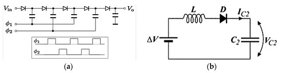
Figure 4. (a) Schematic of the inductor-based CP circuit (b) first stage of the CP [23].
Rumberg et al., in 2017, came up with a new regulated CP circuit, which has designed based on floating-gate transistors. This type of structure is suitable for applications that required tunneling voltages to program floating-gate transistors. Due to its compact architectural design, the CP has leveraged variable frequency regulation and minimized short-circuit current to provide stable tunneling voltages. This design can reduce power dissipation. However, this circuit is not suitable for applications that needed standard CMOS transistors [24].
A high voltage generator based on the CP scheme has demonstrated by Abdi et al. in 2018, which features novel voltage regulation with a variable clock frequency. In this topology, an input voltage modulation has been added to a low-dropout regulator at the input stage to forward the input voltage to the next node. As a result, higher output voltage with stable voltage regulation has been achieved in this method. Moreover, thick-oxide transistors are employed to enhance the pumping efficiency and maintain the substrate/n-well voltage level during operation [25].
Rahman et al. proposed a modified charge transfer switch-based CP circuit in 2020 to be compatible with RFID tag EEPROM as shown in Figure 5. In this design, instead of diode-configuration, all NMOS switches in the charge transfer nodes. As a result, this topology could manage to reduce the substrate current and overall power dissipation. Additionally, in this design, the researchers can minimize the output ripple voltage and the chip layout area. This scheme has also integrated with a voltage regulator to produce a steady-boost voltage, the RFID tag memories requirement [26].
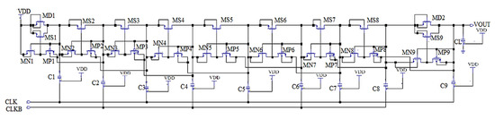
Figure 5. Schematic diagram of the CTS CP [26].
5. CP for Energy Harvesting
In 2008, Richelli et al. proposed a boosted CP design scheme suitable for energy harvesting. It has the feature of increasing output voltage from a very low supply voltage of about 150 mV. This scheme was designed using the new hybrid inductive and capacitive architecture. In particular, this method only consists of NMOS transistors, which were utilized as pass-transistors. Therefore, this scheme has a low threshold voltage compared to a PMOS-based CP circuit [27].
Shih and Otis et al. presented a modified four-phase CP circuit suitable for a fully integrated dc-dc converter for micropower energy harvesting. This modified CP can boost the voltage up to 3xVDD in free-running mode even if the input voltage automatically running down up to 270 mV. To do this autonomous voltage control, this modified CP did not use any external extraction. As a result, this adjusted CP ensured a regulated voltage supply at 1.4 V with only three µW power dissipation. However, this topology was unable to provide higher pumping efficiency with a higher chip area. Simultaneously, this mechanism is not compatible with many applications as the circuit modified to be compatible with DC–DC converter for micropower energy harvesting applications with stringent size constraints [28].
Recently, Peng et al. (2014) proposed a cross-coupled-based CP circuit following the Ker et al. design [29][30].The body biasing and backward charge pump scheme was introduced in this method, which could completely turn off/on the MOS transistors. As a result, voltage loss during switching reduced and the reverse charge sharing problem decreased. Moreover, low voltage operation was arisen due to the involvement of the sub-threshold organization. Nevertheless, two branch CP circuits designed by Peng et al. resolved all the boundaries of the Ker et al. CP circuit, where the pumping effectiveness was found 89% and 0.1 mS pumping speed was delivered. However, this designed CP required 320 mV for start-up, which was higher than other designs with high power dissipation due to its complex circuitry. Moreover, immense leakage current occurred due to unsuitable body biasing and controlling scheme.
Kim et al. (2015) proposed a CP circuit with dynamic body-biasing (DBB) to solve the limitations of high current transfer and high body leakages as shown in Figure 6. In this scheme, dead-time restrictions, conduction loss, and constraints were taking into concern during the design process regarding high voltage adaptation efficacy (VCE) and cut the power conversion efficiency (PCE) of [31].
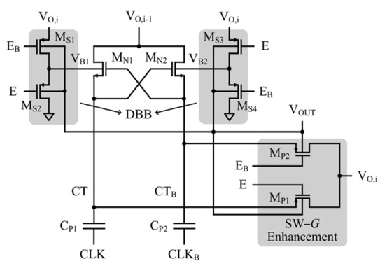
Figure 6. Dynamic-body-biasing CP [31].
In 2016, Mondal et al. proposed an inductor-less switching CP circuit suitable for solar energy harvesting. In this method, the charge transfer capability has improved and the charge sharing time to load. Moreover, in this scheme, a new single-clock tree-topology has been introduced to design the CP circuit, which has provided better charge transfer capability and sharing time. This proposed method has produced higher pumping efficiency for applications like the microscale energy harvesting system [32].
In 2019, Li et al. proposed a temperature-insensitive CP circuit, where the output voltage included a linear adjustment range. In this method, no bipolar-CMOS-DMOS (BCD) technology has been added to generate the output voltage higher than the n-well/substrate diode’s breakdown voltage, which has utilized triple-well NMOS. Besides, the pumping clock’s amplitude has been controlled continuously to produce a closed-loop regulation of voltage to make it insensitive to temperature changes. In a closed-loop control mechanism, the CP output has steady voltage regulation with a voltage deviation of only 1.1%. As a result, the proposed CP scheme has the compatibility of sensor accuracy for controlling micro gyroscopes. No external high voltage device must be integrated with the gyroscope measurement system [33].
References
- Cockcroft, J.D.; Walton, E.T. Experiments with high velocity positive ions. (I) Further developments in the method of obtaining high velocity positive ions. Proc. R. Soc. Lond. 1932, 136, 619–630.
- Pylarinos, L.; Roger, E. Charge Pumps: An Overview; Department of Electrical and Computer Engineering University of Toronto: Toronto, ON, Canada, 2003; p. 7.
- Dickson, J.F. On-chip high-voltage generation in MNOS integrated circuits using an improved voltage multiplier technique. IEEE J. Solid State Circuits 1976, 11, 374–378.
- Witters, J.S.; Groeseneken, G.; Maes, H.E. Analysis and modeling of on-chip high-voltage generator circuits for use in EEPROM circuits. IEEE J. Solid State Circuits 1989, 24, 1372–1380.
- Umezawa, A.; Atsumi, S.; Kuriyama, M.; Banba, H.; Imamiya, K.I.; Naruke, K.; Tanaka, S. A 5-V-only operation 0.6-mu m flash EEPROM with row decoder scheme in triple-well structure. IEEE J. Solid State Circuits 1992, 27, 1540–1546.
- Atsumi, S.; Kuriyama, M.; Umezawa, A.; Banba, H.; Naruke, K.; Yamada, S.; Yoshikawa, K. A 16-Mb flash EEPROM with a new self-data-refresh scheme for a sector erase operation. IEICE Trans. Electron. 1994, 77, 791–799.
- Lauterbach, C.; Weber, W.; Romer, D. Charge sharing concept and new clocking scheme for power efficiency and electromagnetic emission improvement of boosted charge pumps. IEEE J. Solid State Circuits 2000, 35, 719–723.
- Lai, S.Y.; Wang, J.S. A high-efficiency CMOS charge pump circuit. In Proceedings of the IEEE International Symposium on Circuits and Systems Cat. No. 01CH37196, Sydney, NSW, Australia, 6–9 May 2001; Volume 4, pp. 406–409.
- Tanzawa, T.; Tanaka, T.; Takeuchi, K.; Nakamura, H. Circuit techniques for a 1.8-V-only NAND flash memory. IEEE J. Solid State Circuits 2002, 37, 84–89.
- Pelliconi, R.; Iezzi, D.; Baroni, A.; Pasotti, M.; Rolandi, P.L. Power Efficient Charge Pump in Deep Submicron Standard CMOS Technology. IEEE J. Solid State Circuits 2003, 38, 1068–1071.
- Yan, N.; Min, H. A high efficiency all-PMOS charge pump for low-voltage operations. In Proceedings of the 2005 IEEE Asian Solid-State Circuits Conference, Hsinchu, Taiwan, 1–3 November 2005; pp. 361–364.
- Su, L.; Ma, D. Design and optimization of integrated low-voltage low-power monolithic CMOS charge pumps. In Proceedings of the 2008 International Symposium on Power Electronics, Electrical Drives, Automation and Motion, Ischia, Italy, 11–13 June 2008; pp. 43–48.
- Richelli, A.; Colalongo, L.; Tonoli, S.; Kovacs, Z. A 0.2 V–1.2 V converter for power harvesting applications. In Proceedings of the 34th European Solid-State Circuits Conference, Edinburgh, UK, 15–19 September 2008; pp. 406–409.
- Richelli, A.; Mensi, L.; Colalongo, L.; Kovacs, Z.; Rolandi, P.L. A 1.2 V–5 V high efficiency CMOS charge pump for non-volatile memories. In Proceedings of the 2007 IEEE International Symposium on Circuits and Systems, New Orleans, LA, USA, 27–30 May 2007; pp. 2411–2414.
- Richelli, A.; Mensi, L.; Colalongo, L.; Rolandi, P.L.; Kovacs-Vajna, Z.M. A 1.2-to-8 V charge-pump with improved power efficiency for non-volatille memories. In Proceedings of the 2007 IEEE International Solid-State Circuits Conference, San Francisco, CA, USA, 11–15 February 2007; Digest of Technical Papers. pp. 522–619.
- Shiau, M.S.; Hsieh, Z.H.; Hsieh, C.C.; Liu, H.Y.; Liu, D.G. A novel static CTS charge pump with voltage level controller for DC-DC converters. In Proceedings of the 2007 IEEE Conference on Electron Devices and Solid-State Circuits, Tainan, Taiwan, 20–22 December 2007; pp. 481–484.
- Huang, M.-H.; Hsieh, C.-Y.; Fan, P.-C.; Chen, K.-H. A dual-phase charge pump circuit with compact size. Analog. Integr. Circuits Signal Process. 2009, 64, 55–67.
- Peng, F.; Yunlong, L.; Nanjian, W. A high efficiency charge pump circuit for low power applications. J. Semicond. 2010, 31, 015009.
- Wu, J.T.; Chang, Y.H.; Chang, K.L. 1.2 V CMOS switched-capacitor circuits. In Proceedings of the 1996 IEEE International Solid-State Circuits Conference, San Francisco, CA, USA, 10 February 1996; Digest of TEchnical Papers. pp. 388–389.
- Dong-Sheng, L.; Xue-Cheng, Z.; Fan, Z.; Min, D. Embeded EEPROM memory achieving lower power-new design of EEPROM memory for RFID tag IC. IEEE Circuits Devices Mag. 2006, 22, 53–59.
- Yan, L.; Shilin, Z.; Yiqiang, Z. High voltage generator circuit with low power and high efficiency applied in EEPROM. J. Semicond. 2012, 33, 065006.
- Wei, K.C.; Amin, M.S.; Reaz, B. Low voltage charge pump circuit using 0.18 µm CMOS technology. Rev. Roum. Sci. Techn. Électrotechn. Énerg. 2013, 58, 83–92.
- Zucchelli, M.; Colalongo, L.; Richelli, A.; Kovacs-Vajna, Z.M. Dickson charge pump using integrated inductors in complementary metal–oxide semiconductor technology. IET Power Electron. 2016, 9, 553–558.
- Rumberg, B.; Graham, D.W.; Navidi, M.M. A regulated charge pump for tunneling floating-gate transistors. IEEE Trans. Circuit Syst. Express Briefs 2017, 64, 516–527.
- Abdi, A.; Kim, H.S.; Cha, H.K. A High-Voltage Generation Charge-Pump IC using Input Voltage Modulated Regulation for Neural Implant Devices. IEEE Trans. Circuit Syst. Express Briefs 2018, 66, 342–346.
- Rahman, L.F.; Marufuzzaman, M.; Alam, L.; Sidek, L.M.; Reaz, M.B.I. A low power and low ripple CMOS high voltage generator for RFID transponder EEPROM. PLoS ONE 2020, 15, e0225408.
- Richelli, A.; Colalongo, L.; Mensi, L.; Cacciatori, A.; Kovacs-Vajna, Z.M. Charge pump architectures based on dynamic gate control of the pass-transistors. IEEE Trans. Very Large Scale Integr. VLSI Syst. 2009, 17, 964–967.
- Shih, Y.C.; Otis, B.P. An Inductor less DC–DC Converter for Energy Harvesting With a 1.2 µW Bandgap-Referenced Output Controller. IEEE Trans. Circuit Syst. Express Briefs 2011, 58, 832–836.
- Peng, H.; Tang, N.; Yang, Y.; Heo, D. CMOS start-up charge pump with body bias and backward control for energy harvesting step-up converters. IEEE Trans Circuits Syst. Regul. Pap. 2014, 61, 1618–1628.
- Ker, M.D.; Chen, S.L. Ultra-high-voltage charge pump circuit in low-voltage bulk CMOS processes with polysilicon diodes. IEEE Trans. Circuit Syst. Express Briefs 2007, 54, 47–51.
- Kim, J.; Mok, P.K.; Kim, C. A 0.15 V input energy harvesting charge pump with dynamic body biasing and adaptive dead-time for efficiency improvement. IEEE J. Solid State Circuits 2015, 50, 414–425.
- Mondal, S.; Paily, R. An efficient on-chip switched-capacitor-based power converter for a microscale energy transducer. IEEE Trans. Circuit Syst. Express Briefs 2015, 63, 254–258.
- Li, X.; Li, R.; Ju, C.; Hou, B.; Wei, Q.; Zhou, B.; Zhang, R. A Regulated Temperature-Insensitive High-Voltage Charge Pump in Standard CMOS Process for Micromachined Gyroscopes. Sensors 2019, 19, 4149.