+1 credit
| Version | Summary | Created by | Modification | Content Size | Created at | Operation |
|---|---|---|---|---|---|---|
| 1 | Vladimir Drachev | + 2302 word(s) | 2302 | 2019-11-19 10:02:20 | | | |
| 2 | Catherine Yang | -928 word(s) | 1374 | 2019-12-11 07:40:12 | | | | |
| 3 | Catherine Yang | -13 word(s) | 1361 | 2020-10-30 04:16:44 | | | | |
| 5 | Rita Xu | -13 word(s) | 1348 | 2025-01-14 03:23:42 | | | | |
| 6 | Rita Xu | Meta information modification | 1348 | 2025-01-14 03:23:58 | | | | |
| 7 | Rita Xu | Meta information modification | 1348 | 2025-01-14 03:24:33 | | |
Video Upload Options
Researchers briefly review applications of surface-plasmon polariton modes, related to the design and fabrication of electro–optical circuits.
1. Plasmons
A plasmon is defined as a quantum of collective electron oscillation in a solid. It is also referred as a bulk plasmon (Figure 1a). It may reveal itself in metals, doped semiconductors and other materials, where the concentration of charge carriers is sufficient. Charge oscillations near metallic surfaces can be coupled with light, forming surface plasmon polaritons (SPP) [1][2][3] as illustrated in Figure 1b. The localized surface plasmons (LSP) are typical for metallic nanoparticles and rods, where they may also be called transverse plasmons (see Figure 1c). The plasmon observations can be done with electron energy loss spectroscopy (EELS) under excitation by electrons [4], in the extinction optical spectra of small particles and films [5][6], or cathode-luminescence (see [2] and references there). At present time the phenomena of light-matter coupling at the interface between metals and dielectrics is well understood [7]. Traditional applications of LSPs include surface-enhanced Raman spectroscopy (SERS) [8][9], sensing [10][11], scanning near-field optical microscopy (SNOM) and tip-enhanced Raman scattering (TERS) (see [1] and references therein). The SPP modes attract an interest from the point of view of communication due to their subwavelength confinement. This property of SPPs can be extremely useful for applications and allows to bring electronics and photonics closer to each other [12][13][14][15][16][17][18].
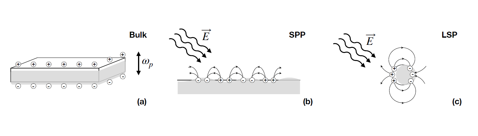
Figure 1. Various types of plasmonic excitations: (a) Bulk plasmon in a metallic sample, electronic gas oscillates as a whole with a plasmonic frequency ωp. (b) Propagating surface plasmon polariton excited by the external electromagnetic wave. (c) Localized surface plasmon excited by the external field in a small metallic nanoparticle. Displacement of the electron gas is shown with light grey.
2. Plasmons at the Interface of Electronics and Photonics
Further achievements in electronics and photonics imply their better integration. Usage of photons at the level of circuits and single chips has a huge potential to improve modern intelligent systems [18]. Along with the usage of light for communication at small and intermediate scales, photonic circuits may also perform logical and computational operations. This implies that the distribution of functions between photons and electrons may be more advanced and potentially more productive than just communication and computation in the future generation of electro–optical chips. Regarding the future of electronics, it is important to note that the development of modern nanofabrication techniques and mesoscopic physics unavoidably leads to molecular electronics, where basic elements of circuits are represented by single molecules [19]. The idea to use both electrons and photons in future “molecular chips”, operated by a microscopically small amount of particles, requires the detailed understanding of their quantum properties and interactions.
The diffraction limit, unbeatable in classical photonics, keeps the size of light processing components at least an order of magnitude larger than the size of the electrical counterpart, i.e., transistors. The typical size of a transistor in modern processors is of the order of 10 nm, while the telecom wavelength of light is close to 1.5 µm. In classical photonics, the electro–optical effect enables a modulation of optical signals due to changes in the optical parameters of materials under applied electric field. This effect is typically not as strong to use it on a chip. The mismatch in dimensions and weak light-matter interaction motivates a search for novel materials and subwavelength optics usage [20].
Traditional plasmonic materials are gold and silver due to the fact that their relaxation constants are less than for other metals (approximately 21 meV for silver and 66 meV for gold [21]). The SPP modes are supported at the interface between dielectrics and noble metals due to the large negative real part of the permittivity of the latter [4]. Metals introduce optical losses, caused by the imaginary part of the permittivity. The resulting damping of surface plasmons limits their practical application. Extra problems are related to interband transitions which result in additional losses. These factors stimulate the search for alternative plasmonic materials with improved properties and the extension to the near-infrared (NIR) including the telecom spectral range [22][23]. Spectral coverage of plasmonic materials were extended also into the deep ultraviolet (UV), where unique plasmon properties have been discovered for ferromagnetic materials as a result of spin-polarization [24]. Alternative plasmonic materials with desired properties applicable in nanophotonics include semiconductors, transparent conductive oxides (TCO) and 2D materials.
The excitation of a SPP requires to reach a certain density of charge carriers. Appropriately doped semiconductors, like Si and GaAs may support plasmonic modes. Silicon plasmonics is discussed in the literature as a platform for on-chip photonics with the SPP propagation length of the order of ten micrometers [25][26]. The advantage of Si is that it is the most common material in electronics with well-developed manufacturing and processing technologies. However, it requires a relatively high level of doping ( 1021 cm−3) to reveal plasmonic properties at telecommunication wavelengths [23].
Another class of materials, commonly referred as transparent conductive oxides, is proven to be useful in plasmonics. Traditional representatives of this class are aluminum-doped zinc oxide (AZO), gallium-doped zinc oxide (GZO) and tin-doped indium oxide (ITO). TCOs show good plasmonic properties in the IR [27]. These materials allow high doping, which makes them conductive [28][29]. At the same time, a large band gap makes them transparent in the visible range. Materials such as ITO are suitable to produce thin films and are compatible with silicon-based components. The excitation of SPPs in ITO has been demonstrated experimentally in the NIR range [30][31]. A relatively low external voltage (below 10 V) applied to ITO can induce a refractive index change of about one (∆n ∼ 1) at telecom wavelengths, which is a desired property in switches and modulators [32].
According to the Drude model, at optical frequencies ω, permittivity reads
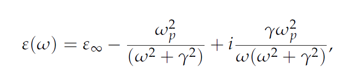
where (ωp)2 = nce2 /(ε0m) is a plasma frequency, γ—relaxation coefficient, ε∞ —asymptotic permittivity at high frequencies, e—electron charge, m—effective electron mass, ε0 —free space permittivity and nc denotes the concentration of charge carriers. The real part of the permittivity may cross zero at certain wavelengths and charge densities. The imaginary part, at the same time, remains finite, which excludes singularities in Maxwell equations. Nevertheless, this epsilon-near-zero (ENZ) point is quite special, since properties of materials vary significantly there [33]. As it was shown experimentally, the Drude model describes ITO quite accurately [34] and the ENZ point is in the IR spectral range. Since the permittivity of ITO depends significantly on the free charge density which enters the plasma frequency, one can locally shift the ENZ wavelength using an external electric field or applying a voltage. The realization of this mechanism in electro–optical devices requires the incorporation of ITO/dielectric capacitors, suitable for charge accumulation. Another approach is to mix TCOs with noble metals to obtain hybrid plasmonic structures with desired properties. For instance, Ag-ITO co-sputtered composite films [35] and thin Au spacer layers incorporated inside ITO films [36] allow to control the ENZ-point wavelength and thus provide better tunability of the system. The development and structuring of metallic/dielectric composites leads to the idea of plasmonic metamaterials supporting the ENZ effect with many intriguing properties, like, for example, optical nonlocality [37].
Surface plasmons can be excited in 2D materials as well. One of the most studied examples is graphene. Optical properties of such structures are obviously qualitatively different from 3D bulk materials or films. The dispersion relation of massless Dirac electrons and its influence on the overall material properties are well known. Plasmonic behavior of graphene can be engineered using geometrical variations, doping and stacking [38][39]. Thus, one of the characteristic features of 2D structures is high tunability. Gating works particularly well there [40]. It is experimentally demonstrated that in graphene/SiO2/Si structures it is possible to alter both the amplitude and wavelength of plasmons by applying a gate voltage [41]. Typical propagation length of the order of micrometers (several plasmon wavelengths) is reported in these experiments. Fast and efficient gating leads to various applications including graphene-based optical transistors and modulators [42]. Fundamental limits of graphene plasmonics due to losses were probed recently in cryogenic experiments, revealing the physics of plasmonic dissipation [43]. At the temperature of liquid nitrogen, when certain mechanisms of dissipation can be excluded, the plasmon propagation length grows and can exceed 10 µm (approximately 50 wavelengths).
References
- Novotny, L.; Hecht, B. Principles of Nano-Optics; Cambridge University Press: Cambridge, UK, 2012.
- Maier, S.A. Plasmonics: Fundamentals and Applications; Springer Science & Business Media: New York, USA, 2007.
- Agranovich, V.; Mills, D. Surface Polaritons; North-Holland Publishing Company: New York, USA, 1982.
- R. H. Ritchie; Plasma Losses by Fast Electrons in Thin Films. Physical Review 1957, 106, 874-881, 10.1103/PhysRev.106.874.
- C. J. Powell; J. B. Swan; Effect of Oxidation on the Characteristic Loss Spectra of Aluminum and Magnesium. Physical Review 1960, 118, 640-643, 10.1103/physrev.118.640.
- Jonathan A. Scholl; Ai Leen Koh; Jennifer A. Dionne; Quantum plasmon resonances of individual metallic nanoparticles. Nature 2012, 483, 421-427, 10.1038/nature10904.
- J M Pitarke; V M Silkin; E V Chulkov; P M Echenique; Theory of surface plasmons and surface-plasmon polaritons. Reports on Progress in Physics 2006, 70, 1-87, 10.1088/0034-4885/70/1/r01.
- Y. -H. Nie; Emory; Probing Single Molecules and Single Nanoparticles by Surface-Enhanced Raman Scattering. Science 1997, 275, 1102-1106, 10.1126/science.275.5303.1102.
- Kneipp, K.; Wang, Y.; Kneipp, H.; Perelman, L.T.; Itzkan, I.; Dasari, R.R.; Feld, M.S.; Single molecule detection using surface-enhanced Raman scattering (SERS). Phys. Rev. Lett. 1997, 78, 1667, https://scholar.harvard.edu/perelman/publications/single-molecule-detection-using-surface-enhanced-raman-scattering-sers.
- Na Liu; Ming L. Tang; Mario Hentschel; Harald Giessen; A. Paul Alivisatos; Nanoantenna-enhanced gas sensing in a single tailored nanofocus. Nature Materials 2011, 10, 631-636, 10.1038/nmat3029.
- M. I. Stockman; Nanoplasmonic sensing and detection. Science 2015, 348, 287-288, 10.1126/science.aaa6805.
- William L. Barnes; Alain Dereux; Thomas W. Ebbesen; Surface plasmon subwavelength optics. Nature 2003, 424, 824-830, 10.1038/nature01937.
- Ekmel Ozbay; Plasmonics: Merging Photonics and Electronics at Nanoscale Dimensions. Science 2006, 311, 189-193, 10.1126/science.1114849.
- Dmitri K. Gramotnev; Sergey I. Bozhevolnyi; Plasmonics beyond the diffraction limit. Nature Photonics 2010, 4, 83-91, 10.1038/nphoton.2009.282.
- Mark I. Stockman; Nanoplasmonics: past, present, and glimpse into future. Optics Express 2011, 19, 22029-22106, 10.1364/oe.19.022029.
- Timothy J. Davis; Daniel E. Gómez; Ann Roberts; Plasmonic circuits for manipulating optical information. Nanophotonics 2016, 6, 543-559, 10.1515/nanoph-2016-0131.
- Ke Liu; Chen Ran Ye; Sikandar Khan; Volker J. Sorger; Review and perspective on ultrafast wavelength-size electro-optic modulators. Laser & Photonics Reviews 2015, 9, 172-194, 10.1002/lpor.201400219.
- David Thomson; Aaron Zilkie; John E Bowers; Tin Komljenovic; Graham T Reed; Laurent Vivien; Delphine Marris-Morini; Eric Cassan; Léopold Virot; Jean-Marc Fédéli; et al.Jean-Michel HartmannJens H SchmidDan-Xia XuFrédéric BoeufPeter O’BrienGoran Z MashanovichM Nedeljkovic Roadmap on silicon photonics. Journal of Optics 2016, 18, 73003, 10.1088/2040-8978/18/7/073003.
- Timothy A. Su; Madhav Neupane; Michael L. Steigerwald; Latha Venkataraman; Colin Nuckolls; Chemical principles of single-molecule electronics. Nature Reviews Materials 2016, 1, 16002, 10.1038/natrevmats.2016.2.
- Mark I Stockman; Katrin Kneipp; Sergey I Bozhevolnyi; Soham Saha; Aveek Dutta; Justus Ndukaife; Nathaniel Kinsey; Harsha Reddy; Urcan Guler; Vladimir M Shalaev; et al.Alexandra BoltassevaBehrad GholipourHarish N S KrishnamoorthyKevin F MacdonaldCesare SociNikolay I ZheludevVassili SavinovRanjan SinghPetra GrosChristoph LienauMichal VadaiMichelle L SolomonDavid R BartonMark LawrenceJennifer A DionneSvetlana V BoriskinaRuben EstebanJavier AizpuruaXiang ZhangSui YangDanqing WangWeijia WangTeri W OdomNicolò AccantoPablo M De RoqueIon M HancuLukasz PiatkowskiNiek F Van HulstMatthias F Kling Roadmap on plasmonics. Journal of Optics 2018, 20, 043001, 10.1088/2040-8986/aaa114.
- P. B. Johnson; R. W. Christy; Optical Constants of the Noble Metals. Physical Review B 1972, 6, 4370-4379, 10.1103/PhysRevB.6.4370.
- P.R. West; Satoshi Ishii; G.V. Naik; N.K. Emani; V.M. Shalaev; A. Boltasseva; Searching for better plasmonic materials. Laser & Photonics Reviews 2010, 4, 795-808, 10.1002/lpor.200900055.
- Gururaj V. Naik; Vladimir M. Shalaev; Alexandra Boltasseva; Alternative Plasmonic Materials: Beyond Gold and Silver. Advanced Materials 2013, 25, 3264-3294, 10.1002/adma.201205076.
- Hari L. Bhatta; Ali E. Aliev; Vladimir P. Drachev; New mechanism of plasmons specific for spin-polarized nanoparticles.. Scientific Reports 2019, 9, 2019, 10.1038/s41598-019-38657-w.
- Richard Soref; Robert E. Peale; Walter Buchwald; Longwave plasmonics on doped silicon and silicides.. Optics Express 2008, 16, 6507-6514, 10.1364/oe.16.006507.
- Jennifer A. Dionne; Luke A. Sweatlock; Matthew T. Sheldon; A. Paul Alivisatos; Harry A. Atwater; Silicon-Based Plasmonics for On-Chip Photonics. IEEE Journal of Selected Topics in Quantum Electronics 2010, 16, 295-306, 10.1109/jstqe.2009.2034983.
- M. A. Noginov; Lei Gu; J. Livenere; G. Zhu; A. K. Pradhan; R. Mundle; M. Bahoura; Yu. A. Barnakov; V. A. Podolskiy; Transparent conductive oxides: Plasmonic materials for telecom wavelengths. Applied Physics Letters 2011, 99, 021101, 10.1063/1.3604792.
- Gregory J. Exarhos; Xiao-Dong Zhou; Discovery-based design of transparent conducting oxide films. Thin Solid Films 2007, 515, 7025-7052, 10.1016/j.tsf.2007.03.014.
- A. K. Kulkarni; Estimation and verification of the electrical properties of indium tin oxide based on the energy band diagram. Journal of Vacuum Science & Technology A: Vacuum, Surfaces, and Films 1996, 14, 1709-1713, 10.1116/1.580324.
- F. Michelotti; Lorenzo Dominici; Emiliano Descrovi; Norbert Danz; Francesca Menchini; Thickness dependence of surface plasmon polariton dispersion in transparent conducting oxide films at 155 μm. Optics Letters 2009, 34, 839-841, 10.1364/ol.34.000839.
- Stefan Franzen; Crissy Rhodes; Marta Cerruti; Ralph W. Gerber; Mark Losego; Jon-Paul Maria; D. E. Aspnes; Plasmonic phenomena in indium tin oxide and ITO-Au hybrid films.. Optics Letters 2009, 34, 2867-2869, 10.1364/ol.34.002867.
- Xinxiang Niu; Xiaoyong Hu; Saisai Chu; Qihuang Gong; Epsilon-Near-Zero Photonics: A New Platform for Integrated Devices. Advanced Optical Materials 2018, 6, p. 1701292, 10.1002/adom.201701292.
- Lucia Caspani; R. P. M. Kaipurath; Matteo Clerici; Marcello Ferrera; T. Roger; J. Kim; N. Kinsey; M. Pietrzyk; A. Di Falco; V. M. Shalaev; et al.A. BoltassevaDaniele Faccio Enhanced Nonlinear Refractive Index in ε -Near-Zero Materials. Physical Review Letters 2016, 116, no, 10.1103/physrevlett.116.233901.
- M. Zahirul Alam; Israel De Leon; Robert W. Boyd; Large optical nonlinearity of indium tin oxide in its epsilon-near-zero region. Science 2016, 352, 795-797, 10.1126/science.aae0330.
- Chaonan Chen; Zhewei Wang; Ke Wu; Hui Ye; Tunable near-infrared epsilon-near-zero and plasmonic properties of Ag-ITO co-sputtered composite films. Science and Technology of Advanced Materials 2018, 19, 174-184, 10.1080/14686996.2018.1432230.
- Xu Fang; Chee Leung Mak; Jiyan Dai; Kan Li; Hui Ye; Chi Wah Leung; ITO/Au/ITO Sandwich Structure for Near-Infrared Plasmonics. ACS Applied Materials & Interfaces 2014, 6, 15743-15752, 10.1021/am5026165.
- Robert Pollard; Antony Murphy; W. R. Hendren; P. R. Evans; R. Atkinson; G. A. Wurtz; A. V. Zayats; Viktor A. Podolskiy; Optical Nonlocalities and Additional Waves in Epsilon-Near-Zero Metamaterials. Physical Review Letters 2009, 102, 127405, 10.1103/physrevlett.102.127405.
- Long Ju; Baisong Geng; Jason Horng; Caglar Girit; Michael Martin; Zhao Hao; Hans A. Bechtel; Xiaogan Liang; Alex Zettl; Y. Ron Shen; et al.Feng Wang Graphene plasmonics for tunable terahertz metamaterials. Nature Nanotechnology 2011, 6, 630-634, 10.1038/nnano.2011.146.
- Hugen Yan; Xuesong Li; Bhupesh Chandra; George Tulevski; Yanqing Wu; Marcus Freitag; Wenjuan Zhu; Phaedon Avouris; Fengnian Xia; Tunable infrared plasmonic devices using graphene/insulator stacks. Nature Nanotechnology 2012, 7, 330-334, 10.1038/nnano.2012.59.
- Jianing Chen; Michela Badioli; Pablo Alonso-González; Sukosin Thongrattanasiri; Florian Huth; Johann Osmond; Marko Spasenović; Alba Centeno; Amaia Pesquera; Philippe Godignon; et al.Amaia Zurutuza ElorzaNicolas CamaraF. Javier García De AbajoRainer HillenbrandFrank H. L. Koppens Optical nano-imaging of gate-tunable graphene plasmons. Nature 2012, 487, 77-81, 10.1038/nature11254.
- Zhe Fei; A. S. Rodin; G. O. Andreev; Wenzhong Bao; A. S. McLeod; M. Wagner; L. M. Zhang; Z. Zhao; M. Thiemens; G. Dominguez; et al.M. M. FoglerA. H. Castro NetoC. N. LauF. KeilmannD. N. Basov Gate-tuning of graphene plasmons revealed by infrared nano-imaging. Nature 2012, 487, 82-85, 10.1038/nature11253.
- Graphene plasmonics; Grigorenko, A.; Polini, M.; Novoselov, K. . Nat. Photonics 2012, 6, 749, https://www.nature.com/articles/nphoton.2012.262.
- G. X. Ni; A. S. McLeod; Z. Sun; L. Wang; L. Xiong; K. W. Post; S. S. Sunku; B.-Y. Jiang; J. Hone; C. R. Dean; et al.M. M. FoglerD. N. Basov Fundamental limits to graphene plasmonics.. Nature 2018, 557, 530-533, 10.1038/s41586-018-0136-9.