Directed self-assembly (DSA) of block copolymers (BCPs) is a bottom-up approach to nanofabrication based on the ability of BCPs to phase separate spontaneously. It is an attractive technique for the fabrication of nanoscale structures thanks to its high resolution, low cost, ease of integration and scalability [1,2,3]. Although DSA has drawn a lot of attention in industrial semiconductor processing since the late 1990s [4,5,6], the main limitation for its incorporation into high-volume manufacturing is its capability to meet industry defect density standards [7,8].
- DSA
- block copolymers
- nanolithography
- directed self-assembly
- graphoepitaxy
- chemoepitaxy
1. Introduction
BCPs are macromolecules consisting of covalently bonded homogeneous blocks of chemically different monomers. Due to the dis-affinity between these blocks, BCPs segregate into microdomains after a thermally-driven phase separation process, generating self-assembled patterns within the nano/microscale [9,10].
Three parameters determine the period, morphology and phase behavior of BCPs when they self-assemble: the total number of monomers forming the BCP (degree of chain polymerization, N), the relative volume fraction of each block (f) and the Flory-Huggins interaction parameter (χ). This parameter gives an idea of how strong the repulsive force between the blocks is [9,11].
The most studied block copolymer is polystyrene-block-poly(methyl methacrylate), PS-b-PMMA, formed by a chain of PS and a chain of PMMA covalently bonded. However, its low value of χ limits minimum attainable resolution (to about 22 nm) [20,12]. Solutions to overcome this come from chain modification [13,14], the use of additives [15] or the pursuit of novel molecular architectures of high-χ BCPs, which combine polymers that are strongly immiscible [16,17].
2. Graphoepitaxy and Chemoepitaxy
In order to be useful for lithographic purposes, BCPs must be someway guided into the desired long-range order and morphology. To do so accurately, templates known as guiding patterns (GPs) are used to direct the self-assembly, whilst BCP properties (molecular weight and composition) and thermodynamics control the feature size, shape and uniformity of the resulting features. As the density of GPs is generally lower than the pitch of the self-assembled microdomains, BCPs are a valuable pattern multiplication method that is able to provide resolution enhancement to pre-patterned templates [18,19].
GPs are normally fabricated by top-down techniques, following two different approaches: chemoepitaxy and graphoepitaxy (Figure 1) [11,20,21]. Chemoepitaxy involves the creation of dense chemical patterns on a neutral substrate to generate preferential wetting sites for one of the blocks [22]. Multiple processes and techniques have been successfully used to selectively tune the surface free energy of a neutral surface, forcing some areas to present more affinity to one of the blocks, including photolithography [23], electron-beam lithography (EBL) and oxygen plasma functionalization [24,25,26,27,28], direct EBL exposure [29] and scanning-probe lithography [30,31,32].
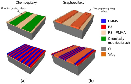
Figure 1. Schematic of DSA by chemo- and graphoepitaxy. (a) In chemoepitaxy, areas of the substrate are chemically activated to show stronger affinity to one of the blocks, directing the self-assembly; (b) in graphoepitaxy, the substrate is topographically structured to direct the self-assembly.
Graphoepitaxy, on the other hand, is based on the definition of 3D features on the substrate, within DSA takes place [33,34,35,36,37]. These topographical templates can be physically tailored, and bottom and walls along the trenches chemically modified to impose different affinity to each of the polymer blocks, enforcing their orientation along the topography [38,39].
3. DSA of BCPs for Nanoelectronics
Line-space pitch multiplication and contact via level patterning are the two pivotal applications of DSA in high-volume manufacturing. In line-space applications lamellar BCPs have been used as mask for the definition of arrays of silicon fins that constitute the central body of non-planar fin field-effect transistors (FinFETs). Multiple works have demonstrated the capability of DSA to fabricate silicon fins [40,41,42], with probably the two most well-known being the LiNe [43,44] and IBM lift-off chemoepitaxial processes [45,46].
Regarding graphoepitaxial approaches, the most common strategy is to use topographical GPs in the shape of trenches, balancing the surface free energy between BCP domains and bottom of the trench, while un-grafted GP walls show stronger affinity to one of the blocks [47,48]. As consequence, when DSA is performed, domains are aligned perpendicularly to the bottom surface and parallel to the walls.
In contact via level patterning cylindrical or lamellar BCPs can be integrated directly into conventional CMOS lithography to generate contact-hole shrinking, contact multiplication or contact uniformity enhancement [49,50]. Firstly, GPs are pre-patterned, followed by dry etching for their structuring. Afterwards, the surface of the cavity that serves as GP is tuned to be attractive to PMMA. Then, the BCP is spin-coated filling the GP and self-assembly is carried out by thermal annealing. Finally, PMMA is etched away, and the remaining PS is used as mask for pattern transfer of shrunk uniform holes [51,52].
The fabrication of silicon vertical structures in the form of nano-sized pillars is another promising target of DSA processes in nanoelectronics. Pillar fabrication has been demonstrated by combination of DSA with tone-inversion [53,54], by sequential infiltration synthesis in BCPs [55,56], and directly by pattern transfer of the BCP template [57]. As we approach the most extreme semiconductor nodes in terms of scaling, alternative architectures and devices such as vertical gate-all-around field-effect transistors (GAA FETs) or single-electron transistors (SETs) are entering into discussion [58], which could be potentially fabricated by DSA.
4. DSA of BCPs for the Fabrication of Functional Structures
Besides DSA for logic, research efforts have also centered their attention on other emerging areas that were looking for large area nanostructuring techniques. Many of these fields are low demanding regarding BCP defectivity levels and, in many cases, self-assembly does not require to be directed, but rather take place on a free surface without guidance.
Applications include hard-disk drive and magnetic storage devices [59,60], nanophotonics and plasmonics materials [61,62], or chemical sensors [63]. Most often, BCPs are still used as templates for patterning, as in the case of graphene structuring [64,65] the fabrication of nanoporous membranes [66,67] or energy storage, photovoltaics and batteries [68,69]. In other applications, however, BCPs can present a more active role and can be used as stabilizing agent, for surface functionalization [70,71] or to aid in nanoparticle self-assembly [72].
A DSA process which enables the fabrication of ultra-thin silicon membranes suspended by high-density arrays of silicon nanowires (SiNWs) has also been demonstrated (Figure 2), with potential to be applied to fabricate nanoelectromechanical systems (NEMS). Each step of the fabrication process is compatible with standard CMOS technology and can be scalable to high-volume manufacturing.
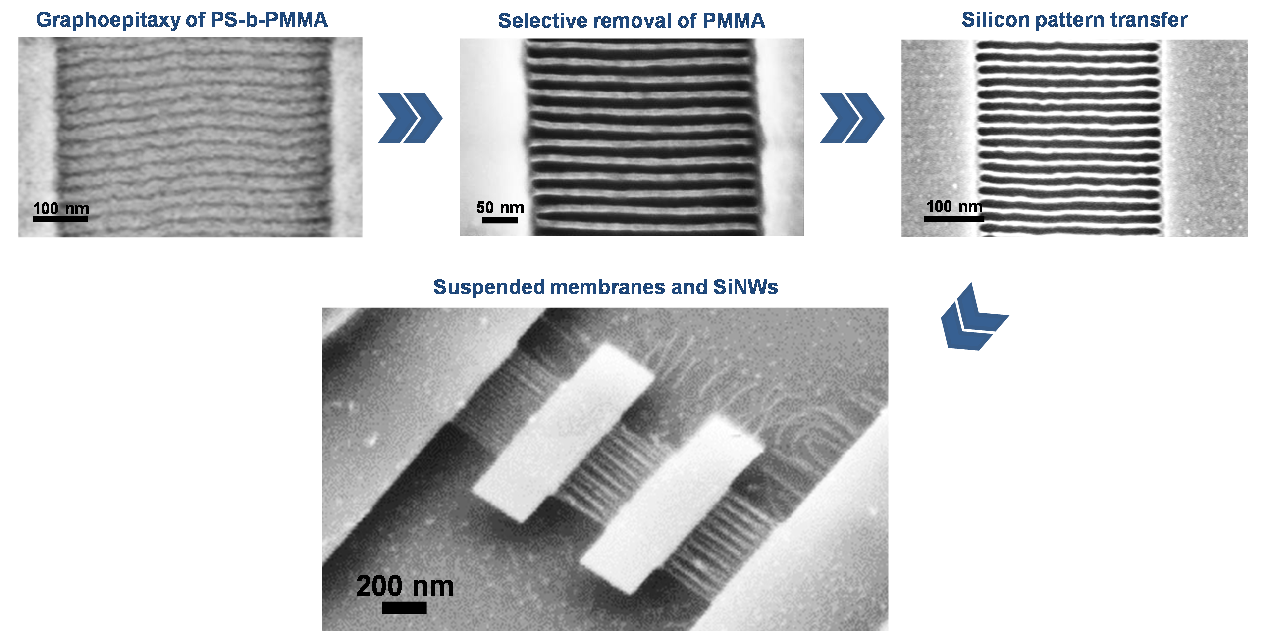
Figure 2. Main steps of the process flow developed for the fabrication of suspended SiNWs and membranes. First, graphoepitaxy of PS-b-PMMA is performed in such a way that lamellae become perpendicular to walls and bottom of silicon oxide GPs; then, PMMA is selectively removed by dry etching; remaining PS and SiO2 are used as mask to define SiNWs and silicon membranes, respectively; finally, structures are released from the BOX in hydrofluoric acid.
This entry is adapted from the peer-reviewed paper 10.3390/polym12102432