Perovskite-based solar cells are a promising photovoltaic technology capable of offering higher conversion efficiency at low costs compared with the standard of the market. They can be produced via a thin film technology that allows for considerable environmental sustainability, thus representing an efficient, sustainable, flexible, and light solution. Tandem solar cells represent the next step in the evolution of photovoltaics (PV). They promise higher power conversion efficiency (PCE) than those currently dominating the market. The tandem solar cell design overcomes the limitations of single junction solar cells by reducing the thermal losses as well as the manufacturing costs. Perovskite has been employed as a partner in different kinds of tandem solar cells, such as the Si and CIGS (copper indium gallium selenide) based cells that, in their tandem configuration with perovskite, can convert light more efficiently than standalone sub-cells.
1. Introduction
In the last few years, the growing interest in substituting fossil-based fuel with renewable energies has pushed up PV technologies towards new materials and designs to improve efficiency and limit costs [
1,
2]. During 2021, all the world’s regions increased solar photovoltaics, despite the tough post-COVID economic context of disrupted supply chains and more expensive solar system components. Data from the International Renewable Energy Agency (IRENA) released on 11 April 2022 show that, at the end of 2021, the installed solar capacity worldwide reached 843.1 GW, with an increase of 133.6 GW, surpassing that of wind, which was 824.9 GW for the same period. Energy prices, already high in the electricity market in 2021, rose even more due to the Russian invasion of Ukraine on 24 February 2022, generating an epochal change in governments’ approach to the energy issue and spurring even more the so-called ecological transition, in which photovoltaics are one of the main protagonists.
Among the many technologies for photovoltaics, crystalline silicon is undoubtedly the most mature and the most commercially suitable for the modern market. For the past several decades, silicon solar cells have been the main driving force in PV technology due to the abundance and environmentally friendly nature of silicon, as well as its high stability and low cost. Nevertheless, this semiconductor suffers from several drawbacks that intrinsically limit cell efficiency. For example, the silicon spectral quantum efficiency and the air mass (AM) solar spectrum do not match; consequently, only a little amount of long wavelength sunlight is absorbed. Typically, the above problem is solved by designing a relatively thick silicon structure that allows for greater photon absorption. However, at the same time, this introduces inevitable conversion efficiency losses due to the non-radiative recombination process of the photo-generated charge carriers that must travel from the depletion region to the electrical contacts. All these constraints, also taking into account the Auger effect, make the maximum practical achievable efficiency about 30% [
3,
4,
5,
6]. One of the potential technologies for next-generation silicon solar cells is the silicon heterojunction (SHJ). When compared with industrial homojunction silicon solar cells, SHJ solar cells exhibit a better power transfer efficiency, lower manufacturing temperatures, and a lower temperature coefficient. The term heterojunction refers to the fact that the P–N junction consists of silicon layers with two different morphologies: a p-type amorphous silicon region and the n-doped crystalline silicon absorber. The first silicon-based heterojunction device was made in 1983 and had an efficiency greater than 12% [
7]. In the early 1990s, Sanyo developed the HIT (heterojunction with intrinsic thin layer) solar cell. Its design dramatically reduces the surface recombination thanks to an amorphous Si buffer layer inserted between the doped emitter and the substrate [
8]. The most recent world record for a silicon solar cell was recently set by the Kaneka Corporation, which obtained an efficiency of up to 26.7% for a 79 cm
2 solar cell [
9]. This finding is approaching the theoretical top limit of 29% for single junction silicon solar cells [
10] and pushes up the research toward novel configurations employing different materials to approach a higher efficiency at lower or at least reasonable costs. A well-known strategy for improving efficiency is the multijunction design that uses multiple junctions, made with different semiconductors each tuned to absorb a different region of the solar spectrum.
Multijunction devices’ topology includes an upper cell made of wider bandgap semiconductors able to catch the high-energy photons, allowing the lower-energy photons to pass through. Then, to capture photons at longer wavelengths, one or more junctions with smaller bandgap semiconductors are placed beneath the top junction. The ultimate theoretical efficiency increases with the number of junctions stacked on top of each other.
Early research into multijunction devices exploited semiconductors such as gallium indium phosphate (GaInP), gallium indium arsenide (GaInAs), and gallium arsenide (GaAs). At present, a 47.1% solar conversion efficiency has been demonstrated using a monolithic, series-connected, six-junction inverted metamorphic structure with alloys of III–V semiconductors and operating under the direct spectrum at 143 suns concentration.
Building these junctions requires the reduction of the threading dislocations in lattice-mismatched III–V alloys, avoiding the phase segregation in metastable quaternary III–V alloys, and controlling the dopant diffusion in complex structures [
11], resulting in a more expensive technology compared with the standard silicon-based one.
Indeed, multijunction devices have mostly been employed in space, where the use of this somewhat expensive solar technology is allowable to reduce weight and dimensions. For terrestrial applications, concentrating optics based on Fresnel lenses may be used to increase power output, lowering the costs. Dual-axis sun tracking is needed when using concentrating optics, which adds to the system’s cost. The literature is teeming with articles describing solar cells with different trick topologies that improve overall efficiency.
Recently, efficiencies of 39.5% have been achieved integrating a thick GaInAs/GaAsP strain-balanced quantum well (QW) into a triple-junction inverted metamorphic multijunction device, consisting of a GaInP upper cell, a GaInAs/GaAsP QW middle cell, and a mismatched lattice GaInAs lower cell [
12].
2. Perovskite/Perovskite Tandem Solar Cells
The realization of the perovskite/perovskite tandem solar cell (PPTSC) is an alternative approach to achieve a high PCE with some advantages, such as simple bandgap tuning of perovskite absorbers, cost-effective and low-temperature monolithic production processes for both the sub-cells, and use of inexpensive precursor materials on flexible substrates [
66,
97,
125,
126].
Interestingly, a detailed balance theory has demonstrated that the PCE of TSC may go beyond 45% using optimum material bandgaps (~1.1 eV and ~1.73 eV) [
10,
127,
128], allowing the prediction of a great advantage in using a monolithic perovskite-based design, as the bandgap of these materials is easily tunable. A key challenge is to save the quality of the lower cell while processing the upper cell. As for SHJ and CIGS, perovskite bottom cells also require processing temperatures below 200 °C, and therefore all contact layers need to be processed at low temperatures. This has been realized in both n–i–p [
126,
129,
130,
131] and p–i–n [
125,
132,
133,
134,
135,
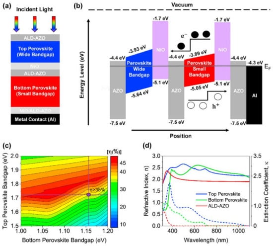
136] sub-cell architectures, the latter one being more frequently used because it allows a better efficiency to be obtained. The first example of PPTSC used two analogue sub-cells with similar absorbing materials: the MA lead iodide (MAPbI
3) and the MAPbBr
3. They were connected with a 2 μm thick doped HTL by a lamination procedure [
137]. Despite the demonstration of a V
OC as high as 2.2 V (that corresponds to the sum of the two sub-cell V
OC), the PCE was limited due to the spectral properties of the absorbing layers, which in turn greatly reduced the overall attainable current density. The PCE was further reduced by the low conductivity of the HTL layer due to its thickness. The HTL transport properties have been improved by Li-TFSI additives that act as hole conductors such as quasi-solid electrolytes because the additives provide Li/Li
+ redox shuttle [
138]. Selecting proper materials with complementary bandgaps, Lin et al. [
132] built a maximum PCE of 24.8% by monolithically fabricating all-perovskite PPTSC. They used 1.22 eV and 1.77 eV bandgap perovskites as bottom and top sub-cells, respectively, demonstrating the perovskite flexibility in terms of bandgap [
132]. A schematic cross-section of the proposed planar PPTSC is shown in
Figure 1. The front contact ETL consists of 50 nm Al-doped ZnO (AZO) followed by a perovskite absorber layer. A double layer of NiO/AZO is utilized as an HTL, where a very thin NiO is used with a 50 nm thick AZO film. Furthermore, the combined NiO/AZO layer works as a tunneling junction, facilitating efficient charge carrier transportation [
139,
140,
141,
142]. Finally, a 100 nm Al is used as a back reflector. Concerning the absorbing layer, the top cell consists of a wide bandgap (Eg~1.72 eV) Cs
yFA
1−yPb(I
xBr
1−x)
3 perovskite with a composition ratio of 0.1, while a low bandgap (Eg~1.16 eV) MASn
xPb
1−xI
3 perovskite with a composition factor of 0.85 is utilized as a bottom cell. As the overall efficiency strongly depends on the electrodes’ transport qualities, some effort has been devoted to improving the ETL layer also. This latter usually consists of a mesoporous–titanium dioxide thin film, which, however, can allow non-radiative recombination at the ETL perovskite interface, worsening the performance. It has been demonstrated that a thin layer of polyacrylic-acid-stabilized tin (IV) oxide quantum dots (paa-QD-SnO
2) on the compact titanium dioxide enhances light capture and widely suppresses nonradiative recombination. Using paa-QD-SnO
2 as the electron-selective contact enabled PSCs (0.08 cm
2) with a PCE of 25.7% (certified 25.4%) and allowed an increase of the PSC areas. Namely, areas of 1.20 and 64 cm
2 were obtained with PCEs of 23.3, 21.7 and 20.6%, respectively [
30].
Figure 1. (
a) Scheme and (
b) corresponding energy levels of the planar perovskite/perovskite tandem solar cell. (
c) Theoretical upper energy conversion efficiency (ECE) limit of two-terminal (2T) monolithic. (
d) Refractive index and extinction coefficient curves (solid and dashed curves, respectively) of large and narrow bandgap perovskites along with ALD Al-doped ZnO (AZO). (Figures reprinted from Hossain et al. [
139], copyright (2023) with permission of Nano Energy).
Another possible strategy proposed to improve the ETL transport properties consists of introducing iodine-doped g-C
3N
4 (ICN) as an additive via a glass-assisted annealing route into ZnTiO
3. The ETL thus obtained has a better crystalline quality and a more adequate alignment of energy levels, and, when used, results in a better PCE [
143]. Some authors have focused their attention on the carrier diffusion length of the perovskite layer that should be many times the absorber thickness to guarantee good PV performance and sufficient charge transport in PSCs [
144,
145]. Unfortunately, diffusion length is mainly limited by grain surface traps, the number of which is very large compared with the number of traps distributed within the grain [
146,
147,
148,
149].
Hence, grain surface passivation has been proposed as a promising route to improve carrier diffusion and PCE [
150,
151,
152], as this strategy overcomes the limits due to the diffusion length, allowing a thicker absorption layer (>1 μm) that, in turn, improves the photons catching. 4-Trifluoromethyl-phenylammonium (CF3-PA) has been used as a strong perovskite surface passivator capable of increasing the diffusion length by up to 5 μm and skyrocketing the PCE to over 26%.CF3-PA passivated tandem devices maintained 90% of their initial PCE after 600 h of operation at the maximum power point under 1 sun illumination in ambient conditions, exhibiting better performance when compared with unpassivated devices [
153]. Another well-known problem of PPTSC concerns the low V
OC, since Br concentrations higher than 20% lead to an increase in the density of traps. In addition, photoinduced halide segregation effects and poor energy alignment with the charge transport layers are possible [
154,
155]. Finally, the interface with the charge transport layers can give rise to localized states within the perovskite bandgap, which, acting as recombination centers, reduce the quantum yield [
156,
157,
158]. The origin of this phenomenon has been attributed to several causes including band misalignment [
158], energy-level pinning [
154], and halide migration from the perovskite into the transport layer [
159]. A typical example of the above issue is the case high performance PPTSC using fullerene ETL that is considered one of the worst offenders regarding the induction of trap states.
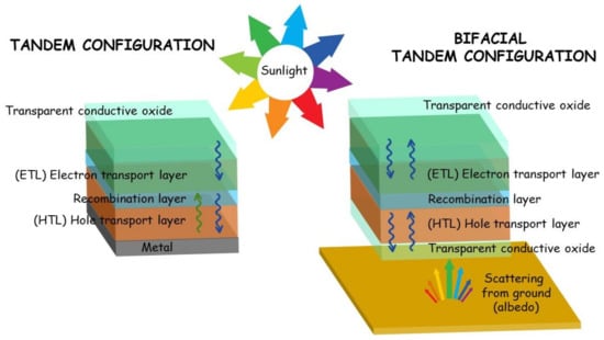
Surface passivation using organic phenethylammonium iodide (PEAI) halide salt [
160] or butylammonium iodide (BA) [
161] and 1,3-propane-diammonium iodide [
162] is a possible strategy proposed to improve PCE by reducing trap states. Recently, bifacial solar cells have attracted the attention of researchers as they can achieve a higher PCE since they can absorb reflected and scattered light (albedo) that achieves the cell’s back-surface (
Figure 2). The main difference consists of using or not using a reflecting layer as the bottom electrode. The possibility of making semitransparent PPTSC represents a great opportunity for the development and application of high-efficiency bifacial cells. In fact, the tandem cells, which can be manufactured using the thin film technology, are excellent candidates because they simultaneously offer a high PCE and a structure that easily allows the lower cell to integrate transparent bottom electrodes, making the cell active also towards the light that comes from below. According to numerical simulation, the benefits of tandem architecture and bifacial design can be inherited by bifacial tandem cells, allowing for higher thermodynamic efficiency than monofacial tandems and single-junction designs [
163,
164].
Figure 2. Scheme of tandem and bifacial tandem configurations.
In 2022, Li and co-workers [
165] developed the first bifacial all-perovskite tandem by using TCO as a rear electrode, starting from an already well known monofacial configuration. The flexibility in designing the perovskite bandgap allowed optimization of the PCE under different realistic illumination and albedo conditions, a PCE > 25% under AM1.5G 1 sun illumination to be obtained. Moreover, in field tests, it is possible to gain a power density as high as 26 mW·cm
−2 [
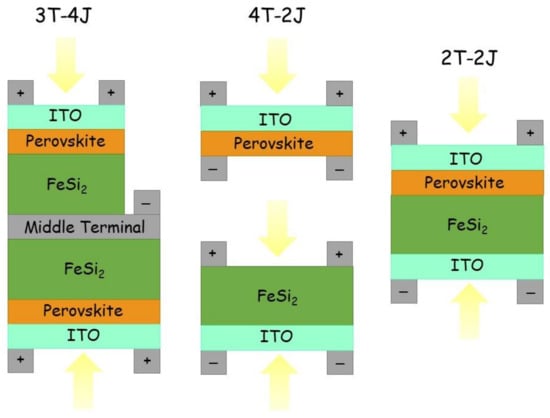
166]. The cell architecture also needs to be investigated; indeed, the thickness of an absorber in a 2T bifacial tandem configuration strongly depends upon the magnitude of albedo due to the current-matching constraint between the sub-cells, while the 4T configuration can work better for a wide range of albedo (
Figure 3) [
167].
Figure 3. Scheme of 3T-4J, 4T-2J, and 2T-2J configurations of bifacial tandem solar cells.
This entry is adapted from the peer-reviewed paper 10.3390/en16083519