1. Introduction
Solar energy is abundant, green and pure in the natural world and thermal and electrical energy may be produced efficiently using solar irradiance [
1].Electrical energy generated through sunlight follows the principle of the photoelectric effect [
2]. According to this principle, an electron-hole pair is generated whenever higher energy photons impinge on the photoactive material [
3]. This in turn is connected through an external circuit to effectively employ the generated electrons. SCs are PV devices which make use of sunlight and convert it into useful electrical energy [
4]. In contrast to fossil fuels, the electrical energy produced from post-manufactured PV devices do not emit CO
2. As a result, solar-powered electricity has minimum impact on the environment. However, conventional energy sources cause the greenhouse effect, global warming, melting of polar ice bergs, gradual rise in sea level, and so on. One of the biggest difficulties with fossil fuels is that their prices are rising at an alarming rate, which brings an opportunity for the speeding up of various cutting edge PV technologies suitable for various industries and consumers [
5]. Hence solar energy is perfectly suited to replace conventional fossil fuels in the near future. Irrespective of solar cells, the refractive index of their different layers plays a vital role in transmission of photons into the depletion region [
6]. In addition, the surface reflection of incident light can be minimized through antireflective thin film coatings [
7]. The selection of antireflective coatings should be based on a refractive index greater than that of the materials involved in interfacial layers of SCs. The reflected photons from the SC surface can be decreased through stronger antireflective films [
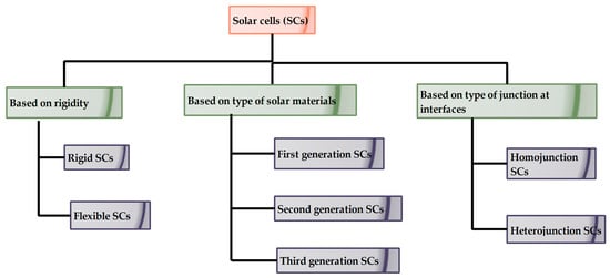
8]. The coating thickness of antireflective films is also determined by the refractive indices of coating material and substrate material. The following flowchart represents the classification of SCs based on various factors.
As shown in
Figure 1, SCs are typically classified by the rigidity of the solar material, i.e., rigid and flexible SCs. At an earlier stage, SCs were developed over rigid substrates, which has several disadvantages such as being somewhat heavier in weight, being difficult to install over any curvatures, and having a higher production cost [
9]. However, rigid Silicon (Si) based SCs possess excellent stability, whilst. flexible thin film SCs are lesser in weight, can be installed over convenient curvatures, can be folded or rolled easily and fabrication cost is less. Stability is a major concern in flexible SCs. Based on the photo-active materials used at various stages, they are classified into first, second and third generation SCs. SCs are also categorized into homojunction and heterojunction SCs depending upon the number of materials that make up the photo-active layer [
10]. Among all SCs, bulk heterojunction hybrid tandem SCs show the maximum PCE. Tandem SCs were developed for overcoming the drawbacks occurring in single material SCs such as the utilization of excess energy of incident light and easier transmission of low energy photons, without participation in the energy conversion process. Some of the commonly observed tandem architectures are two-terminal, mechanically ordered four-terminal and optically coupling four-terminal. With the help of a two-terminal tandem configuration, easier integration with the PV module was achieved than in single junction SCs. In mechanically ordered -terminal SCs, the sub-cells work with their own terminals leading to the non-requirement of the current-matching phenomenon [
11]. Meanwhile, optically coupled tandem architecture was not integrated physically, but the sub-cells were coupled through an optical splitter positioned in an appropriate manner. Integration of sub-cells was more flexible with optically coupled tandem architecture, but costlier due to the inclusion of spectral filters [
12]. In addition to capability in absorbing light which occurs at lower and higher wavelengths, the performance of tandem SCs can further improve through doping of impurities [
2]. Because of the addition of impurities, there is a possibility of tuning the energy band gap of the photo-active layer [
13]. As rigid SCs have been significantly engineered and have captured the entire solar market, we directly review thin film SCs and emerging thin film SCs from various perspectives.
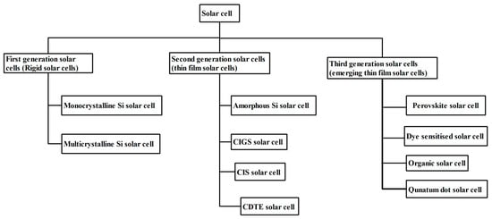
Figure 2 depicts the many generations of SCs as a flowchart.
Figure 1. Classification of SCs based on various factors [
9].
Figure 2. Classification of SCs based on photo-absorber materials.
2. Second Generation Solar Cells
2.1. Amorphous Silicon Solar Cells
As a bon-crystalline direct band-gap semiconducting material, amorphous Si is utilized as a photo-absorber, in the form of light emitting diodes. Amorphous silicon (a-Si) is a non-crystalline form of silicon used for SCs as thin film transistors, used in LED displays. Due to a direct band gap, the incident light becomes absorbed with fewer micrometers of wavelength than for crystalline Si SCs [
14]. For amorphous Si SCs, the tetrahedrally bonded Si atoms are arranged in a disordered fashion [
15].
Due to the disordered nature of the materials, some atoms have dangling bonds. These dangling bonds are considered as defects in the structure of a-Si. The material can be passivated by the hydrogen atoms which bond with the dangling bonds and hence reduces their density. Hydrogenated a-Si (a-Si:H) possess sufficiently less defects and were mostly used in the field of PVs. a-Si:H was initially fabricated in the year 1969 by Chittick, Alexander and Sterling [
16]. The major benefits of hydrogenation of a-Si are much easier fabrication and a much shorter energy payback period. However, hydrogenation leads to the material’s light-induced degradation due to the Steabler-Wronski effect. Hydrogenation also facilitates the possibility of doping in the a-Si:H SC. Furthermore, adding carbon atoms to the a-Si:H might improve the cell’s electrical properties. This addition will lead to the improved transparency of the cell, which results in intensified light trapping and enhanced PCE [
17]. The addition of carbon might also widen the band gap of a-Si:H. The increasing carbon content influences electron mobility, resulting in enhanced disorder in the elemental arrangement. More light can be transmitted into the depletion region of a-Si:H through utilizing TiO
2 nanosphere electrodes which were further coated with ITO in front contact [
18].
The a-Si
x Ge
1-x:H based solar cell is a modified version of the hydrogenated amorphous Si SCs. This type of SC was prone to photosensitivity, with lesser energy band gap. A major drop in performance of a-Si:H due to the Staebler-Wronksi effect was rectified through effective utilization of low band gap material [
19]. By changing the composition of Si and Ge, the energy band gap of SC can be varied from 1.6 eV to 1.1 eV. Hence, absorption of light with longer wavelength was achieved [
20]. Performance further improved through employing back reflectors made of Ag, Au, Al, etc. [
21]
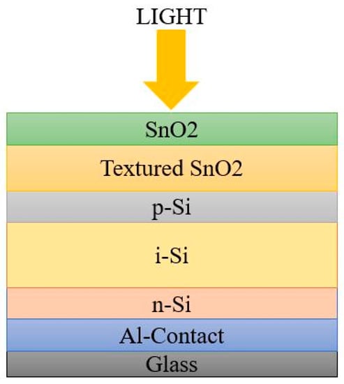
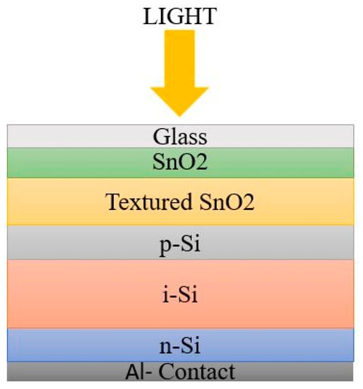
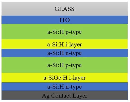
The p-n junction is not enough for efficient charge carrier collection because of the restricted hole mobility, to a certain extent, and of the higher defect density. Hence, an intrinsic absorber layer was introduced between the p- and n- region for charge carrier mobility. The order of arrangement of a-Si:H cell architecture may start with n-type or p-type material. Based on the deposition sequence, there are two possible architectures for a-Si:H cell: superstrate or PiN configuration, and Substrate or NIP configuration [
22,
23].The schematic diagrams in
Figure 3 and
Figure 4 represent the simple architecture of a-Si SC in superstrate and substrate configuration.
Figure 3. Superstrate configuration.
Figure 4. Substrate configuration.
For effective exciton generation and hole collection, the cell is designed in such a way that the light incidence occurs initially only with the p-type material. Typically, the a-Si:H cell architecture consists of TCO, p-type a-Si:H, an intrinsic a-Si:H absorber layer, n- type a-Si:H and metal contact [
23]. In order to obtain better electrical contact for SC, TCO must be the front contact while the back contact may be either conductive metal or TCO. The open circuit voltage was enhanced by a wider bandgap for the active intrinsic absorber layer [
24]. Some foreign elements such as oxygen, carbon, etc., when reinforced with the a-Si:H might also widen the bandgap. The superstrate and substrate were also differentiated by means of transmissivity behavior. The superstrate configuration is most probably temperature resistant and transparent in nature, hence all PIN configurations were preferred for the fabrication of solar modules [
25], but the substrate configuration is opaque in nature and preferred for flexible SCs. There are various thin film-based silicon materials such as nanocrystalline silicon, proto-crystalline silicon and polymorphous silicon. The nanocrystalline silicon (µc-Si:H) has a narrow bandgap material as compared to wider band gap a-Si:H material. Here, the crystallite size varies from a few micro- to nano-meters. The continual nucleation phase of µc-Si:H possesses an undeveloped crystallite structure, known as proto-crystalline silicon (pc-Si:H) [
26]. These are formed by the hydrogen dilution of SiH4, which is much closer to the interfacial phase of a-Si:H to µc-Si:H. Some of the major advantages of pc-Si:H are wider bandgap material and less density. Soon after, the attainment of critical thickness layers always seemed to consist of a microcrystalline structure [
27]. If the silicon is grown in the plasma phase in the intermediate structural appearance, between the a-Si:H and µc-Si:H, then it is known as polymorphous silicon (pm-Si:H) [
28]. During the deposition process, pm-Si:H was deposited over the entire layer depth with uniform homogeneity. Among all other silicon based structures, light induced degradation gives a faster rate for pm-Si:H. Defects of a-Si:H are band-tail state defects and mid-gap defect states [
29]. Doping of foreign elements into the a-Si:H absorber layer might result in a change of fermi level. The heterojunction architecture might also utilize the fraction of unabsorbed incident light, in addition to the absorbed light, for the betterment of PCE in a-Si:H based SC. In a single junction SC, the chance of light absorption is at a particular wavelength, but in a multijunction SC, the cell has a capability to absorb light at varied energy levels [
30].
Figure 5 represents the a-Si:H&a-SiGe:H heterojunction SC, which is capable of converting more photons into electrical energy.
Figure 5. a-Si:H&a-SiGe:H heterojunction SC.
Mid-gap defect states possess sites of effective recombination centers, a major threat to all electronic devices [
31]. Band tail states have been described as some of the energy states which are constrained to a particular extent, but only in between the valence and conduction band.
Table 1 represents a comparison of the various a-Si cells, developed with various materials, along with their output parameters. This is a distribution of Urbach energy exponentially. Some of the advantages of a-Si:H over C-Si are [
32]
-
Simple working mechanism and inexpensive
-
With optimal thickness, light absorption is higher than in the C-Si
-
Lesser raw material is required
-
The capability to adhere over any sort of surfaces.
In addition to these advantages, some of the disadvantages of Si:H SCs are as follows
Table 1. Comparison of PV performance of various a-Si:H based SCs.
| S.No |
Absorber Material |
Voc
(V) |
Jsc
(mA/cm2) |
FF |
eff |
Ref |
| 1 |
μc-Si:H |
0.542 |
27.44 |
73.8 |
10.97 |
[31] |
| 2 |
μc-Si:H |
1.411 |
12.6 |
67.8 |
12.1 |
[34] |
| 3 |
a-Si n type |
0.704 |
42.4 |
82.6 |
24.7 |
[35] |
| 4 |
a-Si:H |
0.877 |
17.28 |
66.6 |
10.09 |
[36] |
| 5 |
μc-Si:H |
0.548 |
29.39 |
73.1 |
11.77 |
[37] |
| 6 |
a-Si:H |
0.896 |
16.36 |
69.8 |
10.22 |
[37] |
| 7 |
μc-Si:H |
1.322 |
13.02 |
69 |
11.9 |
[38] |
| 8 |
a-Si:H μc-Si:H μc-Si:H |
1.936 |
8.96 |
71.5 |
12.41 |
[39] |
| 9 |
μc-Si:H |
0.521 |
28.17 |
71.6 |
10.5 |
[40] |
| 10 |
a-Si:H μc-Si:H μc-Si:H |
1.901 |
9.92 |
72.1 |
13.46 |
[41] |
2.2. CIGS Solar Cell
Because of its higher absorption coefficient, CIGS was employed as primary absorber material with generalized structure as CuIn
(1-x)Ga
xSe
2, similarly to the CdTe architecture. The energy bandgap can be altered by modifying Cd and Ga composition [
42]. The junction behavior of CdS and CIGS with respect to the defects does not cause any major change to the device performance [
43]. The following mathematical equation (1) gives the bandgap of the CIGS with an active material structure Cu In(1-x)GaxSe
2.
For example, if the value of x is 0.1 which might be the composition of Ga, then the energy bandgap was approximated as 1.058 eV. The band gap significantly changes in accordance with the doping level of Ga. In case of CIS, the band gap can be estimated by substituting the value of x as 0, hence the band gap will be 1.01 eV. So, for commercial CIGS, the bandgap varies between 1.01 to 1.1 eV. Their melting point was 985 °C. Generally, CIGS is a p-type material and CdS is a n-type material, which combine together to obtain a p-n junction. In such devices, there is the existence of selenium, which influences the electrical properties of the material [
44]. The presence of four elements makes the fabrication process more challenging.
The CdS in the CIGS SC can be deposited through chemical bath deposition. It can be synthesized with the use of salts such as CdSO
4, CdCl
2, CdI
2, etc., of an aqueous nature. In addition to this complexing agent, NH
3 and thiourea were stirred and heated to optimal temperature and concentration to obtain the CdS material. CdS should be grown in a pseudo-epitaxial manner and seems to be an intermediate structure between polycrystalline and single crystalline structures. At the interface of CdS and CIGS, there is an option of accommodation of the foreign material CdSe, which hinders the cell’s performance. With proper design under optimal conditions, CdSe accumulation can be avoided. In this device, there are also transparent conducting electrodes such as InSnO, SnO
2, which were synthesized through sputtering, evaporation or by atomic layer chemical vapor deposition [
45,
46]. On top of this layer. there is a buffer layer which is probably ZnO, possessing higher resistivity. This in turn reduces the defect intensity at the interfaces and improves the diode quality. It also increases the shunt resistance; hence, the leakage has been reduced. The top contact will be the metal contact with an aluminum grid on top. The various possible fabrication techniques of CIGS SC are evaporation, sputtering, closed space sublimation, spray pyrolysis, chemical bath deposition and the two-step process: metal deposition followed by salinization [
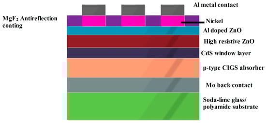
47]. A cross sectional diagram of the CIGS SC, whose cell architecture is glass substrate/Mo/p-type CIGS/n-type CdS/i- ZnO/Zno:Al/MgF
2 ARC/Metal grid, is depicted in
Figure 6. In case of substrate configuration, the light enters through TCO, and over the substrate the back contact material is deposited. For the superstrate configuration, incident light enters through the glass surface and that performs as a window for the photocurrent generation process.
Figure 6. Diagrammatic representation of CIGS cell architecture.
CIGS SCs can be used in place of conventional Si solar cells. In flexible CIGS SCs, which are a multilayered device, a crucial performance inhibitor was interfacial layers, which need to be selected based on stability against mechanical stress, resistance towards temperature and thermal expansion coefficient [
48]. In general, Mo was used as back contact for flexible as well as rigid CIGS SCs. In the case of flexible solar cells, Mo with bigger grains are prone to exert internal minor cracks during plastic deformation of flexible SCs. The thickness of buffer layer CdS also plays a major role in performance of the solar cell. An increase in thickness of the CdS layer facilitates absorption of more photons of shorter wavelength. This leads to a smaller quantity photons reaching the depletion region and is also involved in the power conversion process. In addition to this, the charge carrier mobility of the CdS buffer layer was low compared to the CIGS absorber layer, which also degrades the current conversion efficiency of CIGS SC. Hence, the thickness of buffer layer CdS should be kept as low as possible for the attainment of elevated cell performance [
49].
After the light incidence, the CdS layer of an energy bandgap greater than 2.4 eV allows the photons to reach the absorber layer. The exciton is generated in the active layer. Because of the built-in electric field across the interfaces of p- and n- type material, the generated electrons diffuse into the n-type material and, further, reach the n-electrode, while the generated holes diffuse into the p-type material and then collect at the p-electrode. The back surface field created near the Mo back contact layer helps the escaped electrons to be redirected towards the p-n junction, then reach the n-electrode. Si SC is predominantly used all over the world at present, due to its eases of use and abundant availability compared to other raw materials. Many other alternatives are currently under as effective replacements for Si SC [
50]. CIGS are engineered and used in place of Si SC. They are less prone to mechanical damage compared to Si SCs. The losses incurred with Jsc were rectified by the use of different layers. Monolithic integration during fabrication is not possible with Si SC, but is possible with the CIGS.
Si is an indirect bandgap semiconductor and its absorption coefficient is rather low (104 cm
−1), while CIGS is a direct band gap semiconductor with much higher absorption coefficient. For this reason, CIGS can be fabricated with a thickness as much as 100 times that of Si SC [
51]. The CIGS cell architecture is much similar than that of the tandem SCs, where the high energy photons are absorbed by the CdS layer, while the photons with less energy are simply transmitted to the active layer. There, these latter photons are absorbed, resulting in better utilization of the incident photons. Exciton recombination occurs at the interface of the window buffer layer and the active layer, mainly due to the conduction band discontinuity. The level of discontinuity directly affects the energy bandgap, which increases in accordance with the increase in the discontinuity [
52]. Thin-film flexible SC opens up a new field in the SC market. Flexible substrates are easy to adopt any sort of curvature, lighter in weight and rolled easily. Their production cost is also less and they are likely to be fabricated through Roll-to-Roll manufacturing. Polyimide substrates have been used for flexible CIGS SCs [
53]. There are three different substrates used in CIGS SCs: polymer sheets, ceramics and metallic foils. A higher efficiency of CIGS has been reported with the usage of polyimide substrates
Regarding the chemical composition of CIGS, it is clear that they are a quaternary compound. Uniform constitution of elements over the entire surface of the SC results in optimal photocurrent generation, but attaining uniformity over larger areas is very difficult. For SCs of larger area, PCE is generally low. For large area substrates, sputter coating is most suitable for obtaining uniformity in distribution [
54]. Thickness of the deposited layers and chemical composition can be examined through optical characterization techniques. Coming to the commercialization of long range CIGS, there is a conflict between the size increment and the PCE. These factors cannot be compromised. Cds possess higher toxicity and are harmful to the surrounding environment. As they are toxic, their proper disposal is arduous [
55]. Hence, Cd free CIGS solar panels have been focused on instead. Indium is the key element which is responsible for the price of CIGS panels. The main source of Indium is as a by-product of Zn production. This can be overcome through a preference for flexible, thin, solar CIGS in place of rigid CIGS. without disturbing the PV parameter/Jsc. In addition to this, the time taken to process TCO and CIGS layers seems to be much higher. This should be reduced by adopting a thin CIGS layer and quicker growth techniques [
56].
Table 2 represents a comparison of the various CIGS cells developed with various architectures, along with their output parameters.
Table 2. Comparisons of PV performance of various CIGS based SCs.
| S.No |
Cell Architecture |
Inference |
Voc (V) |
Jsc
(mA cm−2) |
FF
(%) |
Eff
(%) |
Ref |
| 1. |
|
Mo-N back contact diffusion barrier deposition in CIGS SC |
0.622 |
28.67 |
67.53 |
12.05 |
[57] |
| 2. |
|
alkali post deposition treatment of RbF |
0.741 |
37.8 |
80.6 |
22.66 |
[58] |
| 3. |
glass/Mo/CIGS/CdS/i-ZnO/TCO/Au |
CdS buffer layer deposition through chemical bath method, effect of i-ZnO high resistive layer |
0.661 |
32.08 |
78.9 |
15.50 |
[59] |
| 4. |
|
high mobility TCO with 1 eV absorbers |
0.609 |
42.3 |
74.6 |
19.20 |
[60] |
| 5. |
Mo/Si/CIGS/ZnS/ZnO |
impact of silicon inclusion to reduce the cell thickness and influence of thickness and gallium concentration of the CIGS absorber layer on the performance |
0.6903 |
37.57 |
81.03 |
21.08 |
[61] |
| 6. |
ZnO NWs/AZO/ZnS/CIGS/Mo/Thermal electric generator |
enhanced performance achieved by ZnO NWs with CIGS SC along with series connection of Thermal electric generator |
0.85 |
38.55 |
67.2 |
22.02 |
[62] |
| 7. |
(Ni/Al)/MgF2/Al:ZnO/CdS/(KF-PDT/CIGS)/Mo/SLG |
influence of light-soaking, heat-soaking, and combined LS and HS on KF-treated and KF-free CIGS SCs with CBD-CdS buffer layer |
|
|
|
|
[63] |
| 8. |
ZnO/Buffer n-ZnS/p-CIGS/Mo |
effect of ZnS buffer layer |
0.804 |
35.66 |
82.14 |
23.54 |
[64] |
| 9. |
Al2O3/MgF2)/AZO/i-ZnO/CdS/CIGS/Mo |
effect of thickness of ARC over CIGS cell |
|
31.22 |
|
|
[65] |
| 10. |
(Al/Ni)/TCO/CdS/GaOx/CIGS/Mo/Soda-lime glass |
gallium oxide deposited by plasma-enhanced atomic layer deposition, as a surface passivation material at the interface of CdS buffer layer of CIGS SC |
0.056 |
1 |
8.22 |
2.60 |
[66] |
| 11. |
(glass/stainless steel)/Mo/CIGS/CdS/ZnO NWs/ITO |
ZnO NWS incorporated in CIGS and the effect of externally applied stress (rigid) and strain (flexible) |
|
|
|
11.40 (stress) 5.96 (strain) |
[67] |
Some of the major advantages and disadvantages of CIGS SCs are as follows:
-
They are more resistant to heat than Si SCs.
-
The active material (CIGS) does not contain harmful components.
-
Holds easily tunable bandgap, facilitating tandem architecture.
-
Its grain boundaries acts as buffer layer, which inhibits the surface recombination.
Some of the disadvantages of CIGS SCs are:
2.3. CdTe Solar Cell
Cubic tetrahedral crystalline natured CdTe contains Cd and Te with two and six valence electrons and a band gap of 1.44 eV. The obtained band gap is below mono-junction SC’s limiting optical band gap range [
68]. Inclusion of Selenium with the CdTe was also a reason for better performance of this cell [
69]. This was performed by an interdiffusion process with the use of a CdSe precursor, especially at the elevated temperatures of CdTe deposition [
70]. However, selenium, including CdTe via diffusion, find it difficult to absorb light of longer wavelength. Hence CdSe
xTe
1-x synthesized through close space sublimation of about 600 nm thickness increases the ability of long wavelength light absorption, which also results in enhanced PCE. The substrate temperature of CdS deposition has a direct effect on the crystal structure. As the temperature increases, the grain size and crystallinity increases, then interdiffusion is easier for the various layers of semiconductor.
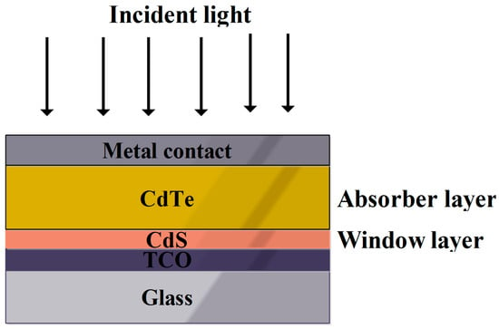
Figure 7 represents the simple cell architecture of the CdTe SC [
71]. The band gap of CdTe is 1.5 eV, which was within the range of photo-absorber material for generating the photocurrent from incident light [
72]. A theoretical efficiency of about 30% was not achieved practically (10–15%) due to various factors, such as the short lifetime of the charge carrier, higher opaqueness of window layer and TCO glass, less stability of doped CdTe films and poor ohmic contact within the interfacial layers of CdTe SC [
73].
Figure 7. Pictorial representation of simple CdTe SC [
74].
In CdTe SCs, conductive, stable and transparent natured TCO was preferred. However, using TCO as front contact of the cell architecture leads to the superstrate configuration as illustrated in
Figure 7 [
74]. The most commonly used materials as TCO were Al doped ZnO(ZnO:Al) and SnO
2:In
2O
3(ITO) in CdTeSCs. The major advantage of these materials are much higher transparency and lower electrical resistance [
74]. The main drawback of ZnO:Al as TCO is that they tend to breakdown easily at temperatures greater than 400 °C. The ITO at higher temperatures also makes the indium diffuse into the CdTe layer. However, the most suitable material at higher process temperatures greater than 500 °C is SnO
2:F, which is commonly known as FTO. Other than these materials, the most suitable alternative, especially for CdTe, is Cd
2SnO
4 [
75].
The CdS is most likely to be used as a window layer in CdTe SCs. The window layer’s main function is collecting the generated excitons from the CdTe active layer. The window layer does not absorb incident light of wavelengths less than 520 nm. Hence there is a degradation in overall performance. The solution for this problem is reducing the thickness of the window layer [
76]. The thickness should not be less than 100 nm, as this might lead to substantial losses in Voc and fill factor. Furthermore, reduction of thickness might create voids in the microstructure of CdS, which also degrades the cell performance. This can be avoided by the implementation of buffer layer between the CdS and CdTe materials. The CdS layer is generally a n-type material and can be deposited through the following techniques: chemical bath deposition, RF sputtering, close space sublimation and thermal evaporation. The oxidized CdS layer presents an increased energy band gap than the actual CdS layer, hence light absorption is further increased. In recent research, an alternative material for CdS is Mg
1−xZnxO (MZO) [
77].
CdTe is a thin film active material which is usually polycrystalline in nature. The PV performance of the absorber layer is usually based on the techniques with which the absorber layer was deposited [
78]. Some of the techniques preferred for the deposition of the active layer are RF sputtering, electrodeposition, thermal evaporation, close space sublimation, etc., and among these, close space sublimation is highly preferred. The major drawback of CdTes is that they hold lower carrier lifetime. Due to the presence of dangling bonds, the interstitial spacing between the grains will act as the active site for the exciton recombination. With the use of characterization techniques such as electron back-scattered diffraction, the level of orientation of grain boundaries, crystalline nature of the deposited film, etc., can be examined [
79].
The design and implementation of back contact in CdTe SC is rather challenging. CdTe is a material with higher ionization potential. Hence, its work function is greater than 5.2 eV for ohmic contact. Lower work function materials lead to the creation of a Schottky junction especially at the interface of CdTe and the metal surface [
80]. Some of the materials whose work function is nearer to the above specified are Ni and Pt, but they readily react with the telluride, hence they remain unusable. Some of the materials with higher dopant densities and better stability are ZnTe, Al doped Te, FeS
2, NiP, etc., capable of forming ohmic contacts. These materials with better ohmic contact can increase the working life of a module by up to 20 years [
81].
CdTe is generally stable in nature. However, some problems were encountered, such as degradation due to improper encapsulation in the cell architecture. Diffusion of copper into the cell architecture also reduces cell performance, which can be overcome through reducing the copper content with the addition of a barrier layer of Zinc Telluride, As
2Te
3 [
82]. In the case of CdTe solar modules, there is no issue with the photo-stability, while in the case of a flexible CdTe cell, more factors affect the stability of the cell. The problem is due mainly to the thin films’ bending, tension and compression. This literature studied the effect of compressive and tensile stresses experienced by thin films installed over different architectures. Thus, efficiencies were not dependent on the substrates, but on stresses (9). CdTe with different substrates has also been studied for the effect of stresses. It is found that the thin film’s polyimide exhibits more incremental distortion than the rigid glass substrate. Polyimide substrates were also easily affected by UV-irradiation, can which can be overcome through anti-UV coatings.
Table 3 gives the comparison of various CdS SCs, along with their cell architectures. Some of the major advantages and disadvantages of CdTeSCs are as follows:
Table 3. Comparison of various CdS SCs along with their cell architectures.
| S.no |
Cell Architecture |
Voc (mV) |
Jsc (mAcm−2) |
FF |
η (%) |
Ref. |
| 1. |
Glass/FTO/n-CdS/n-CdTe/p-CdTe/Au |
730 |
33.8 |
0.62 |
15.30 |
[83] |
| 2. |
Glass/FTO/CdS/CdTe |
838 |
25 |
0.72 |
15.20 |
[84] |
| 3. |
glass/FTO/CdS/CdSe/CdTe/ZnTe:Cu/Au |
791 |
27.4 |
|
13.47 |
[85] |
| 4 |
|
861 |
26.9 |
0.754 |
17.50 |
[71] |
| 5. |
|
863 |
28.6 |
0.781 |
19.25 |
[86] |
| 6. |
Glass/ZnO:Al/n-CdS/p-CdTe/ZnTe |
1528.5 |
28.355 |
0.497 |
21.57 |
[87] |
| 7. |
Glass/n-FTO/n-Cd(S,O)/p-CdTe/p-CuZnTe/Au |
848 |
26.6 |
0.733 |
16.60 |
[88] |
| 8. |
ZnO/CdS/CdTe (0.25/0.05/2.5 micrometers) |
859 |
28.4 |
0.737 |
17.66 |
[89] |
| 9. |
Quartz/Ti/SiO2/CdTe/ITO |
|
40.36 |
|
|
[90] |
| 10. |
Sodalime glass/SnO2:F/SnO2/CdS:O/CdTe/(Cu/Au) |
857 |
23.6 |
0.672 |
14.10 |
[91] |
| 11. |
SiO2/Si(DBR)/ZnTe (BSF)/CdTe/CdS/ZnO/FTO. |
109,820 |
1201 |
0.8203 |
10.39 |
[92] |
| 12. |
glass/SnO2:F(FTO)/n-CdS/p-CdTe/Cu/V2O5/Cu/Au |
806 |
24.8 |
0.7 |
14 |
[84] |
-
The preparation of CdTe SCs was performed in minimal time duration, compared to other SCs.
-
It has a direct band gap with energy of 1.4 eV.
-
It can absorb much shorter wavelengths than silicon solar panels.
-
Raw material Cd was obtained as a sub-product of zinc extraction, hence has less price fluctuation than Si.
Some of the disadvantages of CdTe SCs are:
-
Delivers less power output than Si SCs.
-
Even though Cd was easily available, Te was rarely found in the crust.
-
Cd was highly toxic and its disposal was a rather difficult process
This entry is adapted from the peer-reviewed paper 10.3390/en15228688