Passivation, in physical chemistry and engineering, refers to coating a material so it becomes "passive", that is, less readily affected or corroded by the environment. Passivation involves creation of an outer layer of shield material that is applied as a microcoating, created by chemical reaction with the base material, or allowed to build by spontaneous oxidation in the air. As a technique, passivation is the use of a light coat of a protective material, such as metal oxide, to create a shield against corrosion. Passivation of silicon is used during fabrication of microelectronic devices. In electrochemical treatment of water, passivation reduces the effectiveness of the treatment by increasing the circuit resistance, and active measures are typically used to overcome this effect, the most common being polarity reversal, which results in limited rejection of the fouling layer.[clarification needed] When exposed to air, many metals naturally form a hard, relatively inert surface layer, usually an oxide (termed the "native oxide layer") or a nitride, that serves as a passivation layer. In the case of silver, the dark tarnish is a passivation layer of silver sulfide formed from reaction with environmental hydrogen sulfide. (In contrast, metals such as iron oxidize readily to form a rough porous coating of rust that adheres loosely and sloughs off readily, allowing further oxidation.) The passivation layer of oxide markedly slows further oxidation and corrosion in room-temperature air for aluminium, beryllium, chromium, zinc, titanium, and silicon (a metalloid). The inert surface layer formed by reaction with air has a thickness of about 1.5 nm for silicon, 1–10 nm for beryllium, and 1 nm initially for titanium, growing to 25 nm after several years. Similarly, for aluminium, it grows to about 5 nm after several years. Surface passivation refers to a common semiconductor device fabrication process critical to modern electronics. It is the process by which a semiconductor surface such as silicon is rendered inert, and does not change semiconductor properties when it interacts with air or other materials. This is typically achieved by thermal oxidation, in which the material is heated and exposed to oxygen. In a silicon semiconductor, this process allows electricity to reliably penetrate to the conducting silicon below the surface, and to overcome the surface states that prevent electricity from reaching the semiconducting layer. Surface passivation by thermal oxidation is one of the key features of silicon technology, and is dominant in microelectronics. The surface passivation process was developed by Mohamed M. Atalla at Bell Labs in the late 1950s. It is commonly used to manufacture MOSFETs (metal-oxide-semiconductor field-effect transistors) and silicon integrated circuit chips (with the planar process), and is critical to the semiconductor industry. Surface passivation is also critical to solar cell and carbon quantum dot technologies.
- physical chemistry
- thermal oxidation
- beryllium
1. Mechanisms
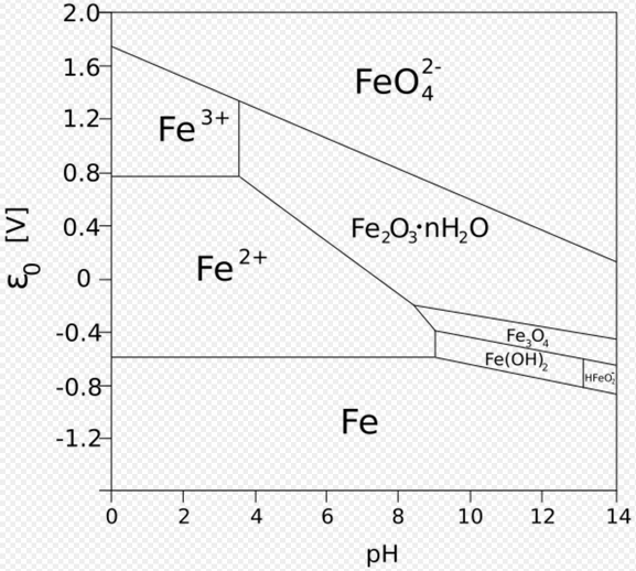
There has been much interest in determining the mechanisms that govern the increase of thickness of the oxide layer over time. Some of the important factors are the volume of oxide relative to the volume of the parent metal, the mechanism of oxygen diffusion through the metal oxide to the parent metal, and the relative chemical potential of the oxide. Boundaries between micro grains, if the oxide layer is crystalline, form an important pathway for oxygen to reach the unoxidized metal below. For this reason, vitreous oxide coatings – which lack grain boundaries – can retard oxidation.[2] The conditions necessary, but not sufficient, for passivation are recorded in Pourbaix diagrams. Some corrosion inhibitors help the formation of a passivation layer on the surface of the metals to which they are applied. Some compounds, dissolved in solutions (chromates, molybdates) form non-reactive and low solubility films on metal surfaces.
2. History
2.1. Discovery
In the mid 1800s, Christian Friedrich Schönbein discovered that when a piece of iron is placed in dilute nitric acid, it will dissolve and produce hydrogen, but if the iron is placed in concentrated nitric acid and then returned to the dilute nitric acid, little or no reaction will take place. Schönbein named the first state the active condition and the second the passive condition. If passive iron is touched by active iron, it becomes active again. In 1920, Ralph S. Lillie measured the effect of an active piece of iron touching a passive iron wire and found that "a wave of activation sweeps rapidly (at some hundred centimeters a second) over its whole length".[3][4]
2.2. Surface Passivation
The surface passivation process was developed by Mohamed M. Atalla at Bell Telephone Laboratories (BTL) in the late 1950s.[5][6] In 1955, Carl Frosch and Lincoln Derick at Bell Telephone Laboratories (BTL) accidentally discovered that silicon dioxide (SiO2) could be grown on silicon. They showed that oxide layer prevented certain dopants into the silicon wafer, while allowing for others, thus discovering the passivating effect of oxidation on the semiconductor surface.[7] In the late 1950s, Atalla further discovered that the formation of a thermally grown SiO2 layer greatly reduced the concentration of electronic states at the silicon surface,[6] and discovered the important quality of SiO2 films to preserve the electrical characteristics of p–n junctions and prevent these electrical characteristics from deteriorating by the gaseous ambient environment.[8] He found that silicon oxide layers could be used to electrically stabilize silicon surfaces.[9] J.R. Ligenza and W.G. Spitzer, who studied the mechanism of thermally grown oxides, managed to fabricate a high quality Si/SiO2 stack, with Atalla and Kahng making use of their findings.[10][11][12] Atalla developed the surface passivation process, a new method of semiconductor device fabrication that involves coating a silicon wafer with an insulating layer of silicon oxide so that electricity could reliably penetrate to the conducting silicon below. By growing a layer of silicon dioxide on top of a silicon wafer, Atalla was able to overcome the surface states that prevented electricity from reaching the semiconducting layer.[5][13] For the surface passivation process, he developed the method of thermal oxidation, which was a breakthrough in silicon semiconductor technology.[14]
Before the development of integrated circuit chips, discrete diodes and transistors exhibited relatively high reverse-bias junction leakages and low breakdown voltage, caused by the large density of traps at the surface of single crystal silicon. Atalla's surface passivation process became the solution to this problem. He discovered that when a thin layer of silicon dioxide was grown on the surface of silicon where a p–n junction intercepts the surface, the leakage current of the junction was reduced by a factor from 10 to 100. This showed that the oxide reduces and stabilizes many of the interface and oxide traps. Oxide-passivation of silicon surfaces allowed diodes and transistors to be fabricated with significantly improved device characteristics, while the leakage path along the surface of the silicon was also effectively shut off. This became one of the fundamental isolation capabilities necessary for planar technology and integrated circuit chips.[15]
Atalla first published his findings in BTL memos during 1957, before presenting his work at an Electrochemical Society meeting in 1958.[16][17] The same year, he made further refinements to the process with his colleagues E. Tannenbaum and E.J. Scheibner, before they published their results in May 1959.[18][19] According to Fairchild Semiconductor engineer Chih-Tang Sah, the surface passivation process developed by Atalla's team "blazed the trail" that led to the development of the silicon integrated circuit.[15][18] Atalla's surface passivation method was the basis for several important inventions in 1959: the MOSFET (MOS transistor) by Atalla and Dawon Kahng at Bell Labs, the planar process by Jean Hoerni at Fairchild Semiconductor, and the monolithic integrated circuit chip by Robert Noyce at Fairchild in 1959.[15][16][17][18] By the mid-1960s, Atalla's process for oxidized silicon surfaces was used to fabricate virtually all integrated circuits and silicon devices.[20]
In solar cell technology, surface passivation is critical to solar cell efficiency.[21] In carbon quantum dot (CQD) technology, CQDs are small carbon nanoparticles (less than 10 nm in size) with some form of surface passivation.[22][23][24]
3. Specific Materials
3.1. Aluminium
Aluminium naturally forms a thin surface layer of aluminium oxide on contact with oxygen in the atmosphere through a process called oxidation, which creates a physical barrier to corrosion or further oxidation in many environments. Some aluminium alloys, however, do not form the oxide layer well, and thus are not protected against corrosion. There are methods to enhance the formation of the oxide layer for certain alloys. For example, prior to storing hydrogen peroxide in an aluminium container, the container can be passivated by rinsing it with a dilute solution of nitric acid and peroxide alternating with deionized water. The nitric acid and peroxide mixture oxidizes and dissolves any impurities on the inner surface of the container, and the deionized water rinses away the acid and oxidized impurities.[25]
Generally, there are two main ways to passivate aluminium alloys (not counting plating, painting, and other barrier coatings): chromate conversion coating and anodizing. Alclading, which metallurgically bonds thin layers of pure aluminium or alloy to different base aluminium alloy, is not strictly passivation of the base alloy. However, the aluminium layer clad on is designed to spontaneously develop the oxide layer and thus protect the base alloy.
Chromate conversion coating converts the surface aluminium to an aluminium chromate coating in the range of 0.00001–0.00004 inches (250–1,000 nm) in thickness. Aluminium chromate conversion coatings are amorphous in structure with a gel-like composition hydrated with water.[26] Chromate conversion is a common way of passivating not only aluminium, but also zinc, cadmium, copper, silver, magnesium, and tin alloys.
Anodizing is an electrolytic process that forms a thicker oxide layer. The anodic coating consists of hydrated aluminium oxide and is considered resistant to corrosion and abrasion.[27] This finish is more robust than the other processes and also provides electrical insulation, which the other two processes may not.
3.2. Ferrous Materials
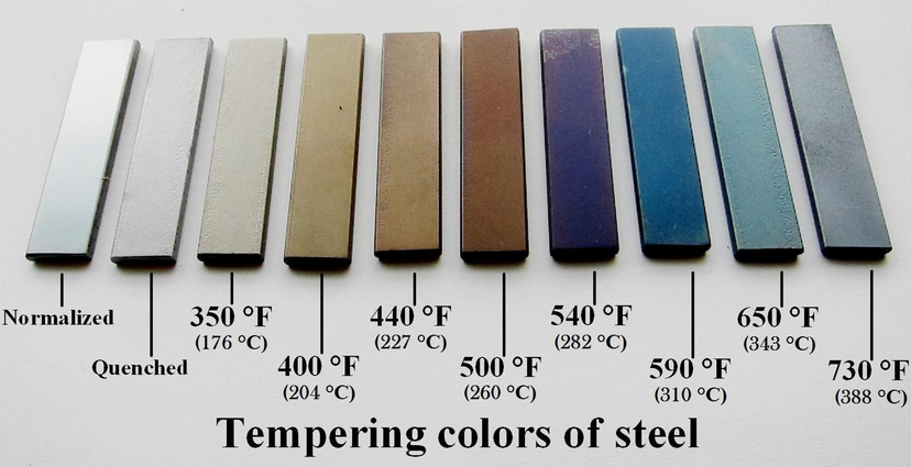
Ferrous materials, including steel, may be somewhat protected by promoting oxidation ("rust") and then converting the oxidation to a metalophosphate by using phosphoric acid and add further protection by surface coating. As the uncoated surface is water-soluble, a preferred method is to form manganese or zinc compounds by a process commonly known as parkerizing or phosphate conversion. Older, less-effective but chemically-similar electrochemical conversion coatings included black oxidizing, historically known as bluing or browning. Ordinary steel forms a passivating layer in alkali environments, as reinforcing bar does in concrete.
Stainless steel
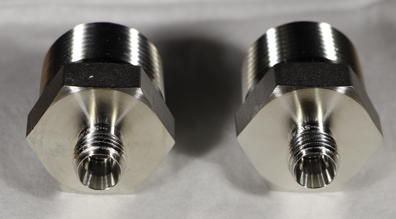
Stainless steels are corrosion-resistant, but they are not completely impervious to rusting. One common mode of corrosion in corrosion-resistant steels is when small spots on the surface begin to rust because grain boundaries or embedded bits of foreign matter (such as grinding swarf) allow water molecules to oxidize some of the iron in those spots despite the alloying chromium. This is called rouging. Some grades of stainless steel are especially resistant to rouging; parts made from them may therefore forgo any passivation step, depending on engineering decisions.[28]
Common among all of the different specifications and types are the following steps: Prior to passivation, the object must be cleaned of any contaminants and generally must undergo a validating test to prove that the surface is 'clean.' The object is then placed in an acidic passivating bath that meets the temperature and chemical requirements of the method and type specified between customer and vendor. While nitric acid is commonly used as a passivating acid for stainless steel, citric acid is gaining in popularity as it is far less dangerous to handle, less toxic, and biodegradable, making disposal less of a challenge. Passivating temperatures can range from ambient to 60 degrees C, or 140 degrees F, while minimum passivation times are usually 20 to 30 minutes. After passivation, the parts are neutralized using a bath of aqueous sodium hydroxide, then rinsed with clean water and dried. The passive surface is validated using humidity, elevated temperature, a rusting agent (salt spray), or some combination of the three.[29] The passivation process removes exogenous iron,[30] creates/restores a passive oxide layer that prevents further oxidation (rust), and cleans the parts of dirt, scale, or other welding-generated compounds (e.g. oxides).[30][31]
Passivation processes are generally controlled by industry standards, the most prevalent among them today being ASTM A 967 and AMS 2700. These industry standards generally list several passivation processes that can be used, with the choice of specific method left to the customer and vendor. The "method" is either a nitric acid-based passivating bath, or a citric acid-based bath, these acids remove surface iron and rust, while sparing the chromium. The various 'types' listed under each method refer to differences in acid bath temperature and concentration. Sodium dichromate is often required as an additive to oxidise the chromium in certain 'types' of nitric-based acid baths, however this chemical is highly toxic. With citric acid, simply rinsing and drying the part and allowing the air to oxidise it, or in some cases the application of other chemicals, is used to perform the passivation of the surface.
It is not uncommon for some aerospace manufacturers to have additional guidelines and regulations when passivating their products that exceed the national standard. Often, these requirements will be cascaded down using Nadcap or some other accreditation system. Various testing methods are available to determine the passivation (or passive state) of stainless steel. The most common methods for validating the passivity of a part is some combination of high humidity and heat for a period of time, intended to induce rusting. Electro-chemical testers can also be utilized to commercially verify passivation.
3.3. Titanium
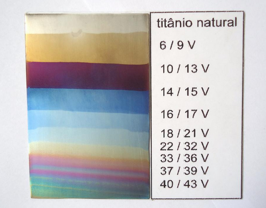
Titanium can be anodised to produce a passivation layer of titanium oxide. As with many other metals, this layer causes thin-film interference which makes the metal surface appear coloured, with the thickness of the passivation layer directly effecting the colour produced.
3.4. Nickel
Nickel can be used for handling elemental fluorine, owing to the formation of a passivation layer of nickel fluoride. This fact is useful in water treatment and sewage treatment applications.
3.5. Silicon
In the area of microelectronics and photovoltaics surface passivation is usually implemented by oxidation to a coating of silicon dioxide. The effect of passivation on the efficiency of solar cells ranges from 3-7%. Passivation is effected by thermal oxidation at 1000 °C. The surface resistivity is high, >100 Ωcm.[32]
The content is sourced from: https://handwiki.org/wiki/Engineering:Passivation
References
- University of Bath & Western Oregon University http://people.bath.ac.uk/chsataj/CHEY0016%20Lecture%2015.htm
- Fehlner, Francis P, ref.3.
- Lillie, Ralph S. (June 20, 1920). "The Recovery of Transmissivity in Passive Iron Wires as a Model of Recovery Processes in Irritable Living Systems". The Journal of General Physiology (Physiological Laboratory, Clark University, Worcester.) 3 (2): 129–43. doi:10.1085/jgp.3.2.129. PMID 19871851. PMC 2140424. http://europepmc.org/backend/ptpmcrender.fcgi?accid=PMC2140407&blobtype=pdf. Retrieved 15 August 2015.
- Macinnes, Duncan A. (1939). The principles of electrochemistry. Reinnhold Publishing Corporation. pp. 447–451.
- "Martin (John) M. Atalla". 2009. https://www.invent.org/inductees/martin-john-m-atalla.
- Black, Lachlan E. (2016). New Perspectives on Surface Passivation: Understanding the Si-Al2O3 Interface. Springer. p. 17. ISBN 9783319325217. https://books.google.com/books?id=laYFDAAAQBAJ&pg=PA17.
- Bassett, Ross Knox (2007). To the Digital Age: Research Labs, Start-up Companies, and the Rise of MOS Technology. Johns Hopkins University Press. pp. 22–23. ISBN 9780801886393. https://books.google.com/books?id=UUbB3d2UnaAC&pg=PA22.
- Saxena, A (2009). Invention of integrated circuits: untold important facts. International series on advances in solid state electronics and technology. World Scientific. p. 96. ISBN 9789812814456. https://books.google.com/books?id=z7738Wq-j-8C.
- Lécuyer, Christophe; Brock, David C. (2010). Makers of the Microchip: A Documentary History of Fairchild Semiconductor. MIT Press. p. 111. ISBN 9780262294324. https://books.google.com/books?id=LaZpUpkG70QC&pg=PA111.
- Huff, Howard R.; Gösele, U.; Tsuya, H. (1998) (in en). Silicon Materials Science and Technology: Proceedings of the Eighth International Symposium on Silicon Materials Science and Technology. The Electrochemical Society. ISBN 978-1-56677-193-1. https://books.google.com/books?id=cr8FPGkiRS0C&pg=PA183.
- Lojek, Bo. (2007). History of semiconductor engineering. Berlin: Springer. ISBN 978-3-540-34258-8. OCLC 317626839. https://www.worldcat.org/oclc/317626839.
- Morris, Peter Robin (1990) (in en). A History of the World Semiconductor Industry. IET. ISBN 978-0-86341-227-1. https://books.google.com/books?id=rslXJmYPjGIC&pg=PA43.
- "Dawon Kahng". https://www.invent.org/inductees/dawon-kahng.
- Huff, Howard (2005). High Dielectric Constant Materials: VLSI MOSFET Applications. Springer Science & Business Media. p. 34. ISBN 9783540210818. https://books.google.com/books?id=kaSmXepnqCMC&pg=PA34.
- Wolf, Stanley (March 1992). "A review of IC isolation technologies". Solid State Technology: 63. http://go.galegroup.com/ps/anonymous?id=GALE%7CA12308297.
- Lojek, Bo (2007). History of Semiconductor Engineering. Springer Science & Business Media. pp. 120& 321–323. ISBN 9783540342588. https://archive.org/details/historysemicondu00loje_697.
- Bassett, Ross Knox (2007). To the Digital Age: Research Labs, Start-up Companies, and the Rise of MOS Technology. Johns Hopkins University Press. p. 46. ISBN 9780801886393. https://books.google.com/books?id=UUbB3d2UnaAC&pg=PA46.
- Sah, Chih-Tang (October 1988). "Evolution of the MOS transistor-from conception to VLSI". Proceedings of the IEEE 76 (10): 1280–1326 (1290). doi:10.1109/5.16328. ISSN 0018-9219. Bibcode: 1988IEEEP..76.1280S. http://www.dejazzer.com/ece723/resources/Evolution_of_the_MOS_transistor.pdf. "Those of us active in silicon material and device research during 1956–1960 considered this successful effort by the Bell Labs group led by Atalla to stabilize the silicon surface the most important and significant technology advance, which blazed the trail that led to silicon integrated circuit technology developments in the second phase and volume production in the third phase.".
- Atalla, M.; Tannenbaum, E.; Scheibner, E. J. (1959). "Stabilization of silicon surfaces by thermally grown oxides". The Bell System Technical Journal 38 (3): 749–783. doi:10.1002/j.1538-7305.1959.tb03907.x. ISSN 0005-8580. https://dx.doi.org/10.1002%2Fj.1538-7305.1959.tb03907.x
- Donovan, R. P. (November 1966). "The Oxide-Silicon Interface". Fifth Annual Symposium on the Physics of Failure in Electronics: 199–231. doi:10.1109/IRPS.1966.362364. https://dx.doi.org/10.1109%2FIRPS.1966.362364
- Black, Lachlan E. (2016). New Perspectives on Surface Passivation: Understanding the Si-Al2O3 Interface. Springer. ISBN 9783319325217. https://core.ac.uk/download/pdf/156698511.pdf.
- null
- Fernando, K. A. Shiral; Sahu, Sushant; Liu, Yamin; Lewis, William K.; Guliants, Elena A.; Jafariyan, Amirhossein; Wang, Ping; Bunker, Christopher E. et al. (2015). "Carbon Quantum Dots and Applications in Photocatalytic Energy Conversion". ACS Applied Materials & Interfaces 7 (16): 8363–76. doi:10.1021/acsami.5b00448. PMID 25845394. https://dx.doi.org/10.1021%2Facsami.5b00448
- Gao, Xiaohu; Cui, Yuanyuan; Levenson, Richard M; Chung, Leland W K; Nie, Shuming (2004). "In vivo cancer targeting and imaging with semiconductor quantum dots". Nature Biotechnology 22 (8): 969–76. doi:10.1038/nbt994. PMID 15258594. https://dx.doi.org/10.1038%2Fnbt994
- Aluminum Passivation [1]
- Chemical Conversion Coating on Aluminum [2]
- Aluminum Anodizing Process [3]
- "Stainless Steel Passivation". Arrow Cryogenics. http://www.arrowcryogenics.com/stainless-steel-passivation.htm.
- "Carpenter Technical Articles - HOW TO PASSIVATE STAINLESS STEEL PARTS". http://www.cartech.com/techarticles.aspx?id=1566.
- "Stainless Steel Passivation Services - A967 & A380 | Delstar Metal Finishing, Inc". http://www.delstar.com/stainless-steel-passivation.
- "Pickling and Passivating Stainless Steel". Euro Inox. http://www.euro-inox.org/pdf/map/Passivating_Pickling_EN.pdf.
- 3.0.CO;2-D. https://dx.doi.org/10.1002%2F1099-159X%28200009%2F10%298%3A5%3C473%3A%3AAID-PIP337%3E3.0.CO%3B2-D" id="ref_32">Aberle, Armin G. (2000). "Surface passivation of crystalline silicon solar cells: A review". Progress in Photovoltaics: Research and Applications 8 (5): 473–487. doi:10.1002/1099-159X(200009/10)8:5<473::AID-PIP337>3.0.CO;2-D. https://dx.doi.org/10.1002%2F1099-159X%28200009%2F10%298%3A5%3C473%3A%3AAID-PIP337%3E3.0.CO%3B2-D