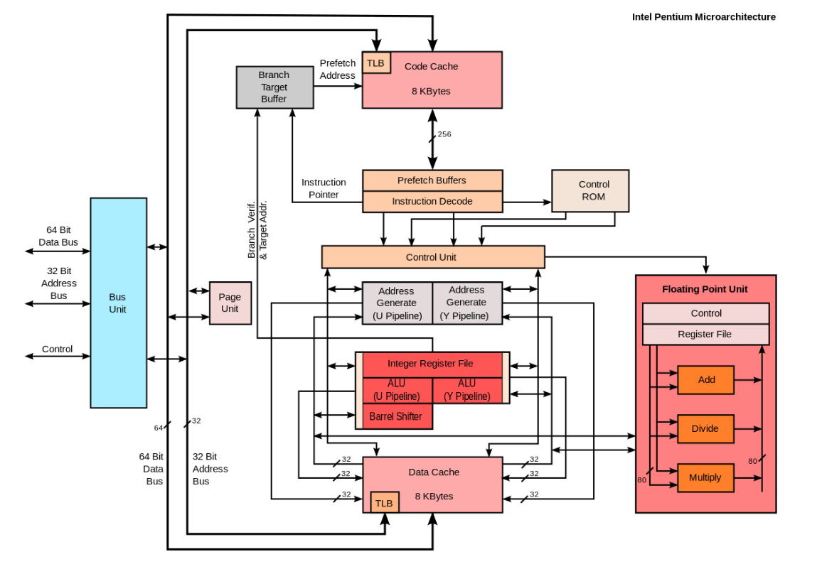
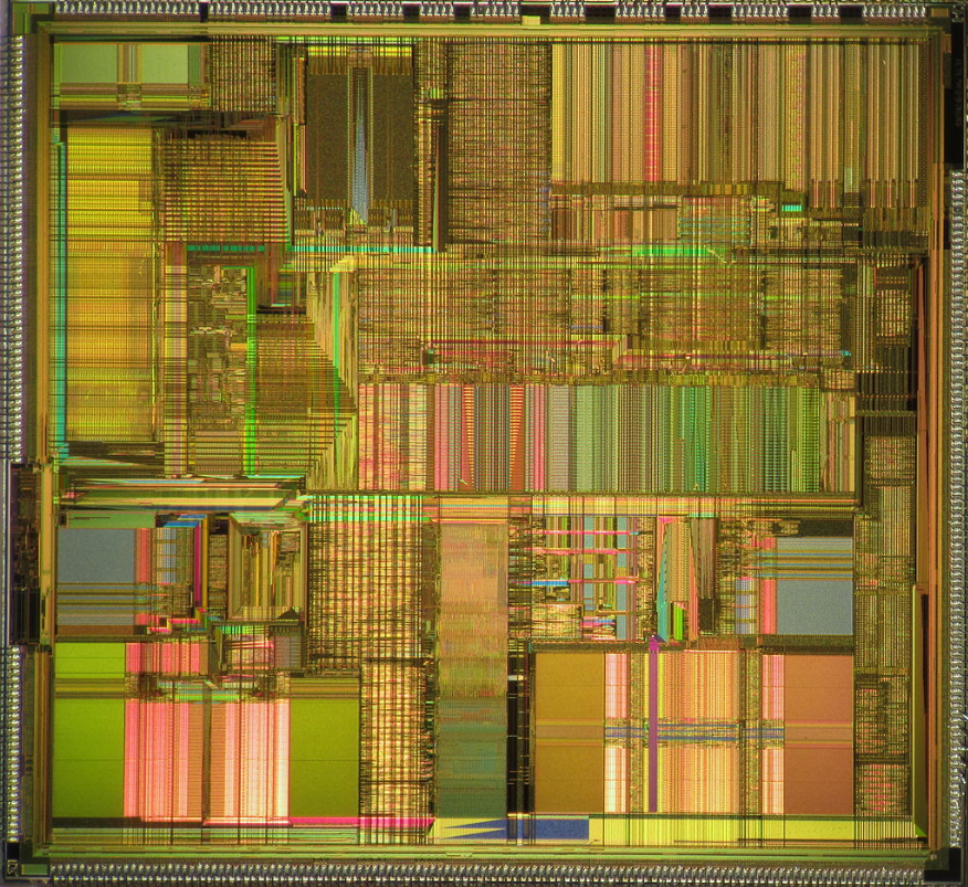
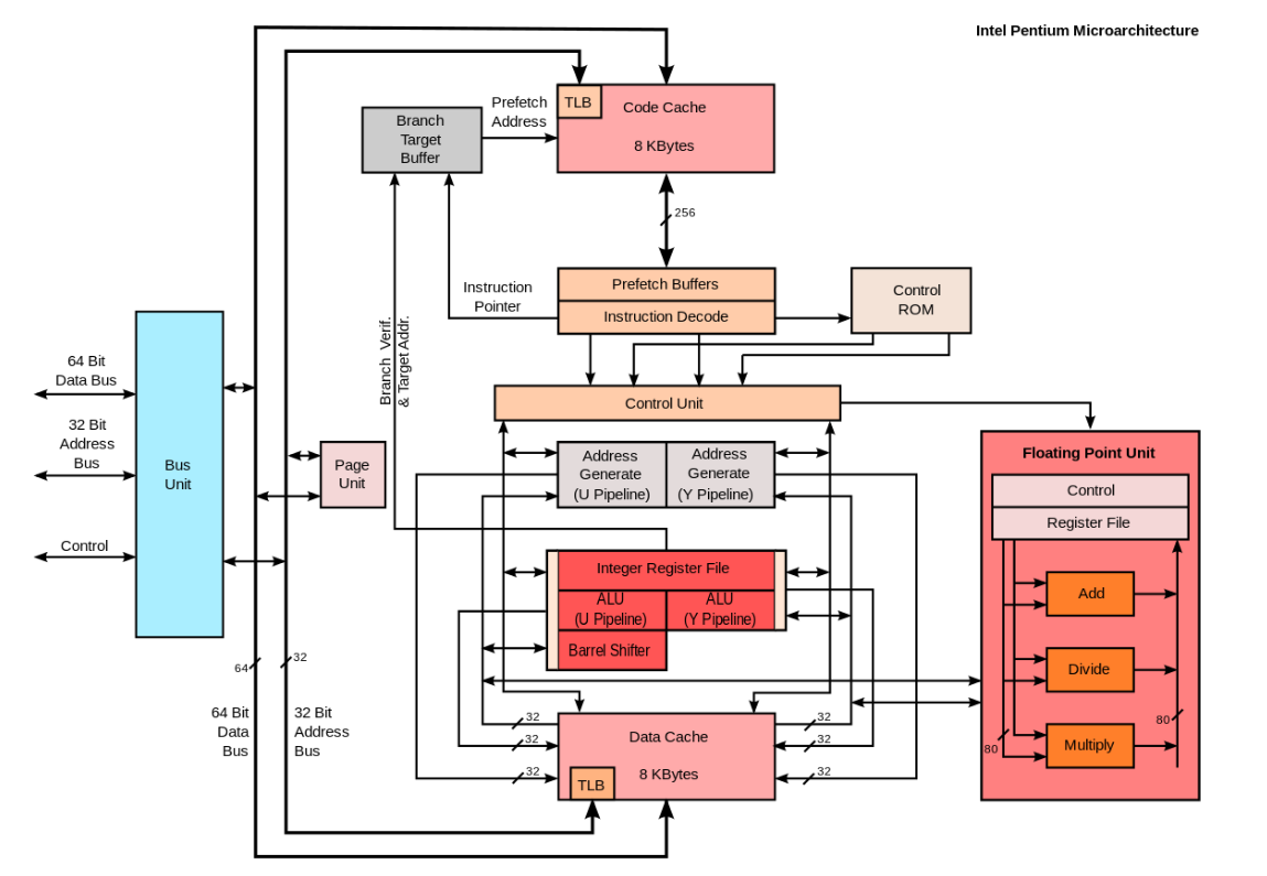
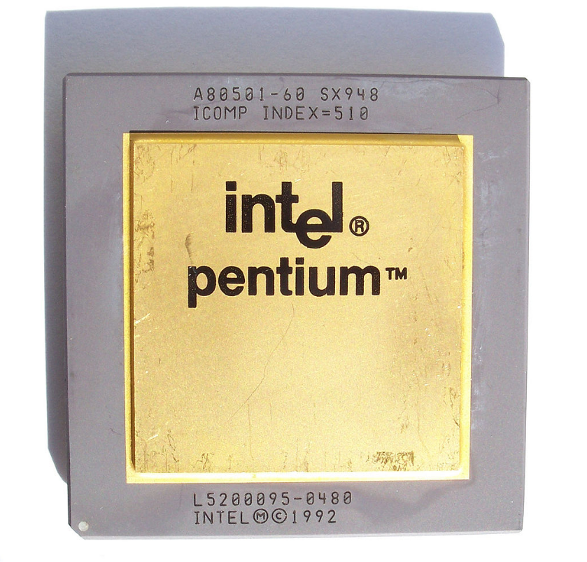
The original Pentium microprocessor was introduced by Intel on March 22, 1993. It was instruction set compatible with the 80486 but was a new and very different microarchitecture design. The P5 Pentium was the first superscalar x86 microarchitecture and the world’s first superscalar microprocessor to be in mass production. It included dual integer pipelines, a faster floating-point unit, wider data bus, separate code and data caches as well as many other techniques and features to enhance performance and support security, encryption, and multiprocessing for workstations and servers. Considered the fifth main generation in the 8086 compatible line of processors, its implementation and microarchitecture was called P5. As with all new processors from Intel since the Pentium, some new instructions were added to enhance performance for specific types of workloads. The Pentium was the first Intel x86 to build in robust hardware support for multiprocessing similar to that of large IBM mainframe computers. Intel worked closely with IBM to define this capability and then Intel designed it into the P5 microarchitecture. This new capability was not present in prior x86 generations or x86 copies from competitors. In order to realize its greatest potential, compilers had to be optimized to take advantage of the instruction level parallelism provided by the new superscalar dual pipelines and applications needed to be recompiled. Intel spent substantial effort and resources working with development tool vendors, and major ISV and OS companies to optimize their products for Pentium prior to product launch. In October 1996, the similar Pentium MMX was introduced, complementing the same basic microarchitecture with the MMX instruction set, larger caches, and some other enhancements. Competitors included Motorola 68040, Motorola 68060, PowerPC 601, SPARC, MIPS, Alpha families, most of which also used a superscalar in-order dual instruction pipeline configuration at some time. Intel discontinued the P5 Pentium processors (sold as a cheaper product since the Pentium II of 1997) in early 2000 in favor of the Celeron processor, which had also replaced the 80486 brand.
- celeron
- superscalar
- parallelism
1. Development
The P5 microarchitecture was designed by the same Santa Clara team which designed the 386 and 486.[1] Design work started in 1989;[2] the team decided to use a superscalar architecture, with on-chip cache, floating-point, and branch prediction. The preliminary design was first successfully simulated in 1990, followed by the laying-out of the design. By this time, the team had several dozen engineers. The design was taped out, or transferred to silicon, in April 1992, at which point beta-testing began.[3] By mid-1992, the P5 team had 200 engineers.[4] Intel at first planned to demonstrate the P5 in June 1992 at the trade show PC Expo, and to formally announce the processor in September 1992,[5] but design problems forced the demo to be cancelled, and the official introduction of the chip was delayed until the spring of 1993.[6][7]
John H. Crawford, chief architect of the original 386, co-managed the design of the P5,[8] along with Donald Alpert, who managed the architectural team. Dror Avnon managed the design of the FPU.[9] Vinod K. Dham was general manager of the P5 group.[10]
Intel's Larrabee multicore architecture project uses a processor core derived from a P5 core (P54C), augmented by multithreading, 64-bit instructions, and a 16-wide vector processing unit.[11] Intel's low-powered Bonnell microarchitecture employed in early Atom processor cores also uses an in-order dual pipeline similar to P5.[12]
1.1. Major Improvements Over the 80486 Microarchitecture
The P5 microarchitecture brings several important advancements over the preceding i486 architecture.
- Performance:
- Superscalar architecture — The Pentium has two datapaths (pipelines) that allow it to complete two instructions per clock cycle in many cases. The main pipe (U) can handle any instruction, while the other (V) can handle the most common simple instructions. Some RISC proponents had argued that the "complicated" x86 instruction set would probably never be implemented by a tightly pipelined microarchitecture, much less by a dual-pipeline design. The 486 and the Pentium demonstrated that this was indeed possible and feasible.
- 64-bit external databus doubles the amount of information possible to read or write on each memory access and therefore allows the Pentium to load its code cache faster than the 80486; it also allows faster access and storage of 64-bit and 80-bit x87 FPU data.
- Separation of code and data caches lessens the fetch and operand read/write conflicts compared to the 486. To reduce access time and implementation cost, both of them are 2-way associative, instead of the single 4-way cache of the 486. A related enhancement in the Pentium is the ability to read a contiguous block from the code cache even when it is split between two cache lines (at least 17 bytes in worst case).
- Much faster floating-point unit. Some instructions showed an enormous improvement, most notably FMUL, with up to 15 times higher throughput than in the 80486 FPU. The Pentium is also able to execute a FXCH ST(x) instruction in parallel with an ordinary (arithmetical or load/store) FPU instruction.
- Four-input address adders enables the Pentium to further reduce the address calculation latency compared to the 80486. The Pentium can calculate full addressing modes with segment-base + base-register + scaled register + immediate offset in a single cycle; the 486 has a three-input address adder only, and must therefore divide such calculations between two cycles.
- The microcode can employ both pipelines to enable auto-repeating instructions such as REP MOVSW perform one iteration every clock cycle, while the 80486 needed three clocks per iteration (and the earliest x86 chips significantly more than the 486). Also, optimization of the access to the first microcode words during the decode stages helps in making several frequent instructions execute significantly more quickly, especially in their most common forms and in typical cases. Some examples are (486→Pentium, in clock cycles): CALL (3→1), RET (5→2), shifts/rotates (2–3→1).
- A faster, fully hardware-based multiplier makes instructions such as MUL and IMUL several times faster (and more predictable) than in the 80486; the execution time is reduced from 13–42 clock cycles down to 10–11 for 32-bit operands.
- Virtualized interrupt to speed up virtual 8086 mode.
- Other features:
- Enhanced debug features with the introduction of the Processor-based debug port (see Pentium Processor Debugging in the Developers Manual, Vol 1).
- Enhanced self-test features like the L1 cache parity check (see Cache Structure in the Developers Manual, Vol 1).
- New instructions: CPUID, CMPXCHG8B, RDTSC, RDMSR, WRMSR, RSM.
- Test registers TR0–TR7 and MOV instructions for access to them were eliminated.
- The later Pentium MMX also added the MMX instruction set, a basic integer SIMD instruction set extension marketed for use in multimedia applications. MMX could not be used simultaneously with the x87 FPU instructions because the registers were reused (to allow fast context switches). More important enhancements were the doubling of the instruction and data cache sizes and a few microarchitectural changes for better performance.
The Pentium was designed to execute over 100 million instructions per second (MIPS),[13] and the 75 MHz model was able to reach 126.5 MIPS in certain benchmarks.[14] The Pentium architecture typically offered just under twice the performance of a 486 processor per clock cycle in common benchmarks. The fastest 80486 parts (with slightly improved microarchitecture and 100 MHz operation) were almost as powerful as the first-generation Pentiums, and the AMD Am5x86 was roughly equal to the Pentium 75 regarding pure ALU performance.
1.2. Errata
The early versions of 60–100 MHz P5 Pentiums had a problem in the floating-point unit that resulted in incorrect (but predictable) results from some division operations. This flaw, discovered in 1994 by professor Thomas Nicely at Lynchburg College, Virginia, became widely known as the Pentium FDIV bug and caused embarrassment for Intel, which created an exchange program to replace the faulty processors.
In 1997, another erratum was discovered that could allow a malicious program to crash a system without any special privileges, the "F00F bug". All P5 series processors were affected and no fixed steppings were ever released, however contemporary operating systems were patched with workarounds to prevent crashes.
2. Cores and Steppings
The Pentium was Intel's primary microprocessor for personal computers during the mid-1990s. The original design was reimplemented in newer processes and new features were added to maintain its competitiveness as well as to address specific markets such as portable computers. As a result, there were several variants of the P5 microarchitecture.
2.1. P5
The first Pentium microprocessor core was code-named "P5". Its product code was 80501 (80500 for the earliest steppings Q0399). There were two versions, specified to operate at 60 MHz and 66 MHz respectively, using Socket 4. This first implementation of the Pentium used a traditional 5-volt power supply (descended from the usual TTL logic compatibility requirements). It contained 3.1 million transistors and measured 16.7 mm by 17.6 mm for an area of 293.92 mm2.[15] It was fabricated in a 0.8 μm BiCMOS process.[16] The 5-volt design resulted in relatively high energy consumption for its operating frequency when compared to the directly following models.
2.2. P54C
The P5 was followed by the P54C (80502) in 1994, with versions specified to operate at 75, 90, or 100 MHz using a 3.3 volt power supply. Marking the switch to Socket 5, this was the first Pentium processor to operate at 3.3 volts, reducing energy consumption, but necessitating voltage regulation on mainboards. As with higher-clocked 486 processors, an internal clock multiplier was employed from here on to let the internal circuitry work at a higher frequency than the external address and data buses, as it is more complicated and cumbersome to increase the external frequency, due to physical constraints. It also allowed two-way multiprocessing and had an integrated local APIC as well as new power management features. It contained 3.3 million transistors and measured 163 mm2.[17] It was fabricated in a BiCMOS process which has been described as both 0.5 μm and 0.6 μm due to differing definitions.[17]
2.3. P54CQS
The P54C was followed by the P54CQS in early 1995, which operated at 120 MHz. It was fabricated in a 0.35 μm BiCMOS process and was the first commercial microprocessor to be fabricated in a 0.35 μm process.[17] Its transistor count is identical to the P54C and, despite the newer process, it had an identical die area as well. The chip was connected to the package using wire bonding, which only allows connections along the edges of the chip. A smaller chip would have required a redesign of the package, as there is a limit on the length of the wires and the edges of the chip would be further away from the pads on the package. The solution was to keep the chip the same size, retain the existing pad-ring, and only reduce the size of the Pentium's logic circuitry to enable it to achieve higher clock frequencies.[17]
2.4. P54CS
The P54CQS was quickly followed by the P54CS, which operated at 133, 150, 166 and 200 MHz, and introduced Socket 7. It contained 3.3 million transistors, measured 90 mm2 and was fabricated in a 0.35 μm BiCMOS process with four levels of interconnect.
2.5. P24T
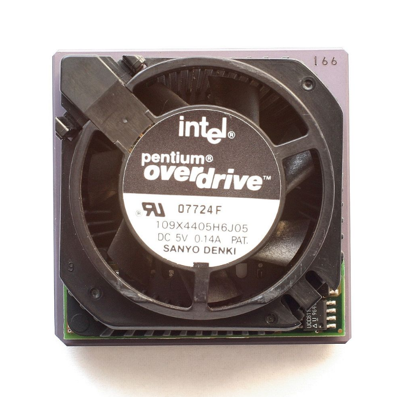
The P24T Pentium OverDrive for 486 systems were released in 1995, which were based on 3.3 V 0.6 μm versions using a 63 or 83 MHz clock. Since these used Socket 2/3, some modifications had to be made to compensate for the 32-bit data bus and slower on-board L2 cache of 486 motherboards. They were therefore equipped with a 32 KB L1 cache (double that of pre-P55C Pentium CPUs).
2.6. P55C


The P55C (or 80503) was developed by Intel's Research & Development Center in Haifa, Israel. It was sold as Pentium with MMX Technology (usually just called Pentium MMX); although it was based on the P5 core, it featured a new set of 57 "MMX" instructions intended to improve performance on multimedia tasks, such as encoding and decoding digital media data. The Pentium MMX line was introduced on October 22, 1996, and released in January 1997.[18]
The new instructions worked on new data types: 64-bit packed vectors of either eight 8-bit integers, four 16-bit integers, two 32-bit integers, or one 64-bit integer. So, for example, the PADDUSB (Packed ADD Unsigned Saturated Byte) instruction adds two vectors, each containing eight 8-bit unsigned integers together, elementwise; each addition that would overflow saturates, yielding 255, the maximal unsigned value that can be represented in a byte. These rather specialized instructions generally require special coding by the programmer for them to be used.
Other changes to the core include a 6-stage pipeline (vs. 5 on P5) with a return stack (first done on Cyrix 6x86) and better parallelism, an improved instruction decoder, 16KB L1 data cache + 16KB L1 instruction cache with Both 4-way associativity (vs. 8KB L1 Data/instruction with 2-way on P5), 4 write buffers that could now be used by either pipeline (vs. one corresponding to each pipeline on P5) and an improved branch predictor taken from the Pentium Pro,[19][20] with a 512-entry buffer (vs. 256 on P5).[21]
It contained 4.5 million transistors and had an area of 140 mm2. It was fabricated in a 0.28 μm CMOS process with the same metal pitches as the previous 0.35 μm BiCMOS process, so Intel described it as "0.35 μm" because of its similar transistor density.[22] The process has four levels of interconnect.[22]
While the P55C remained compatible with Socket 7, the voltage requirements for powering the chip differ from the standard Socket 7 specifications. Most motherboards manufactured for Socket 7 prior to the establishment of the P55C standard are not compliant with the dual voltage rail required for proper operation of this CPU (2.9 volt core voltage, 3.3 volt I/O voltage). Intel addressed the issue with OverDrive upgrade kits that featured an interposer with its own voltage regulation.
2.7. Tillamook
Pentium MMX notebook CPUs used a "mobile module" that held the CPU. This module was a PCB with the CPU directly attached to it in a smaller form factor. The module snapped to the notebook motherboard, and typically a heat spreader was installed and made contact with the module. However, with the 0.25 μm Tillamook Mobile Pentium MMX (named after a city in Oregon), the module also held the 430TX chipset along with the system's 512 KB SRAM cache memory.
3. Models and Variants
  |
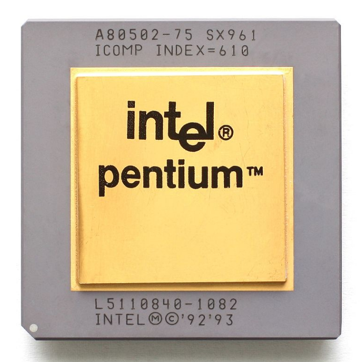 80px 80px 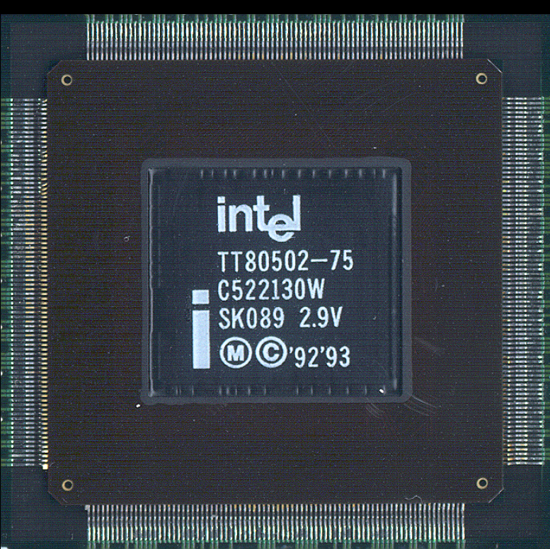 |
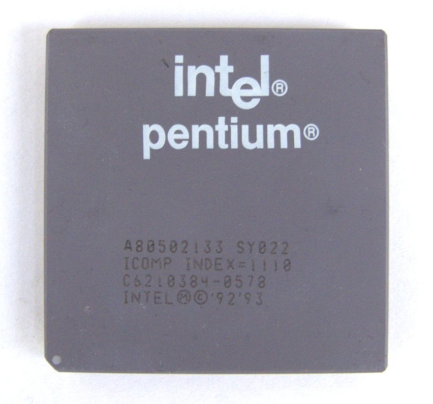 80px 80px  |
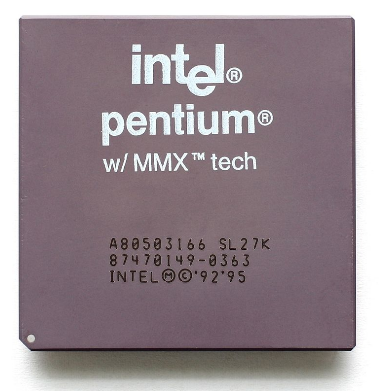 80px 80px  |
 |
||||||||||||||||||
| Code name | P5 | P54C | P54C/P54CQS | P54CS | P55C | Tillamook | ||||||||||||||||
| Product code | 80501 | 80502 | 80503 | |||||||||||||||||||
| Process size (μm) | 0.80 | 0.60 or 0.35* | 0.35 | 0.35 (later 0.28) | 0.25 | |||||||||||||||||
| Die area (mm2) | 293.92 (16.7 x 17.6 mm) | 148 @ 0,6 μm / 91 (later 83) @ 0,35 μm | 91 (later 83) | 141 @ 0,35 μm / 128 @ 0,28 μm | 94.47 (9.06272 x 10.42416 mm) | |||||||||||||||||
| Number of transistors (millions) | 3.10 | 3.20 | 3.30 | 4.50 | ||||||||||||||||||
| Socket | Socket 4 | Socket 5/7 | Socket 7 | |||||||||||||||||||
| Package | CPGA/CPGA+IHS | CPGA/CPGA+IHS/TCP* | CPGA/TCP* | CPGA/TCP* | CPGA/PPGA | PPGA | TCP* | CPGA/PPGA/TCP* | PPGA/TCP* | TCP/TCP on MMC-1 | ||||||||||||
| Clock speed (MHz) | 60 | 66 | 75 | 90 | 100 | 120 | 133 | 150 | 166 | 200 | 120* | 133* | 150* | 166 | 200 | 233 | 166 | 200 | 233 | 266 | 300 | |
| Bus speed (MHz) | 60 | 66 | 50 | 60 | 50 | 66 | 60 | 66 | 60 | 66 | 60 | 66 | 60 | 66 | ||||||||
| Core Voltage | 5.0 | 5.15 | 3.3 2,9* | 3.3 2.9* | 3.3 3.1* 2.9* | 3.3 3.1* 2.9* | 3.3 3.1* 2.9* | 3.3 3.1* 2.9* | 3.3 | 3.3 | 2.2* | 2.45* | 2.45* | 2.8 2.45* | 2.8 | 2.8 | 1.9 1.8* | 1.8* | 1.8* | 1.9 2.0* | 2.0* | |
| I/O Voltage | 5.0 | 5.15 | 3.3 | 3.3 | 3.3 | 3.3 | 3.3 | 3.3 | 3.3 | 3.3 | 3.3 | 3.3 | 3.3 | 3.3 | 3.3 | 3.3 | 2.5 | 2.5 | 2.5 | 2.5 | 2.5 | |
| TDP (max. W) | 14.6 (15.3) | 16.0 (17.3) | 8.0 (9.5) 6.0* (7.3*) | 9.0 (10.6) 7.3* (8.8*) | 10.1 (11.7) 8.0 at 0.6μ* (9.8 at 0.6μ*) 5.9 at 0.35μ* (7.6 at 0.35μ*) | 12.8 (13.4) 7.1* (8.8*) | 11.2 (12.2) 7.9* (9.8*) | 11.6 (13.9) 10.0* (12.0*) | 14.5 (15.3) | 15.5 (16.6) | 4.2* | 7.8* (11.8*) | 8.6* (12.7*) | 13.1 (15.7) 9.0* (13.7*) | 15.7 (18.9) | 17.0 (21.5) | 4.5 (7.4) 4.1* (5.4*) | 5.0* (6.1*) | 5.5* (7.0*) | 7.6 (9.2) 7.6* (9.6*) | 8.0* | |
| Introduced | 1993-03-22 | 1994-10-10 | 1994-03-07 | 1995-03-27 | 1995-06-12 | 1996-01-04 | 1996-06-10 | 1997-10-20 | 1997-05-19 | 1997-01-08 | 1997-06-02 | 1997-08 | 1998-01 | 1999-01 | ||||||||
| * An asterisk indicates that these were only available as Mobile Pentium or Mobile Pentium MMX chips for laptops. | ||||||||||||||||||||||
 |
|||||||
| Code name | P54CTB | ||||||
| Product code | PODPMT60X150 | PODPMT66X166 | PODPMT60X180 | PODPMT66X200 | |||
| Process size (μm) | 0.35 | ||||||
| Socket | Socket 5/7 | ||||||
| Package | CPGA with heatsink, fan and voltage regulator | ||||||
| Clock speed (MHz) | 125 | 150 | 166 | 150 | 180 | 200 | |
| Bus speed (MHz) | 50 | 60 | 66 | 50 | 60 | 66 | |
| Upgrade for | Pentium 75 | Pentium 90 | Pentium 100 and 133 | Pentium 75 | Pentium 90, 120 and 150 | Pentium 100, 133 and 166 | |
| TDP (max. W) | 15.6 | 15.6 | 15.6 | 18 | |||
| Voltage | 3.3 | 3.3 | 3.3 | 3.3 | |||
 |
|||||||
| Code name | P55C | Tillamook | |||||
| Product code | FV8050366200 | FV8050366233 | FV80503CSM66166 | GC80503CSM66166 | GC80503CS166EXT | FV80503CSM66266 | GC80503CSM66266 |
| Process size (μm) | 0.35 | 0.25 | |||||
| Clock speed (MHz) | 200 | 233 | 166 | 166 | 166 | 266 | 266 |
| Bus speed (MHz) | 66 | 66 | 66 | 66 | 66 | 66 | 66 |
| Package | PPGA | PPGA | PPGA | BGA | BGA | PPGA | BGA |
| TDP (max. W) | 15.7 | 17 | 4.5 | 4.1 | 4.1 | 7.6 | 7.6 |
| Voltage | 2.8 | 2.8 | 1.9 | 1.8 | 1.8 | 1.9 | 2.0 |
4. Competitors
After the introduction of the Pentium, competitors such as NexGen,[23] AMD, Cyrix, and Texas Instruments announced Pentium-compatible processors in 1994.[24] CIO magazine identified NexGen's Nx586 as the first Pentium-compatible CPU,[25] while PC Magazine described the Cyrix 6x86 as the first. These were followed by the AMD K5, which was delayed due to design difficulties. AMD later bought NexGen in order to help design the AMD K6, and Cyrix was purchased by National Semiconductor.[26] Later processors from AMD and Intel retain compatibility with the original Pentium.
The content is sourced from: https://handwiki.org/wiki/Engineering:P5_(microarchitecture)
References
- p. 1, The Pentium Chronicles: The People, Passion, and Politics Behind Intel's Landmark Chips, Robert P. Colwell, Wiley, 2006, ISBN:978-0-471-73617-2.
- p. 88, "Inside Intel", Business Week, #3268, June 1, 1992.
- "The hot new star of microchips", Monica Horten, New Scientist, #1871, pp. 31 ff., May 1, 1993. Accessed on line June 9, 2009. http://www.iptegrity.com/index.php?option=com_content&task=view&id=34&Itemid=42
- p. 89, "Inside Intel", Business Week, #3268, June 1, 1992.
- p. 8, "Intel to offer a peek at its `586' chip", Tom Quinlan, InfoWorld, March 16, 1992.
- p. 1, "Design woes force Intel to cancel 586 chip demo", Tom Quinlan and Cate Corcoran, InfoWorld 14, #24, June 15, 1992.
- pp. 1, 103, "P5 chip delay won't alter rivals' plans", Tom Quinlan, InfoWorld 14, #30, July 27, 1992.
- p. 54, "Intel Turns 35: Now What?", David L. Margulius, InfoWorld, July 21, 2003, ISSN 0199-6649.
- p. 21, "Architecture of the Pentium microprocessor", D. Alpert and D. Avnon, IEEE Micro, 13, #3 (June 1993), pp. 11–21, doi:10.1109/40.216745. http://ieeexplore.ieee.org/xpls/abs_all.jsp?arnumber=216745
- p. 90, "Inside Intel", Business Week, #3268, June 1, 1992.
- §3 of Seiler, L.; Cavin, D.; Espasa, E.; Grochowski, T.; Juan, M.; Hanrahan, P.; Carmean, S.; Sprangle, A. et al. (August 2008). "Larrabee: A Many-Core x86 Architecture for Visual Computing". ACM Transactions on Graphics. Proceedings of ACM SIGGRAPH 2008 27 (3): 18:11. doi:10.1145/1360612.1360617. ISSN 0730-0301. http://download-software.intel.com/sites/default/files/m/9/4/9/larrabee_manycore.pdf. Retrieved August 6, 2008.
- Anand Lal Shimpi (January 27, 2010), Why Pine Trail Isn't Much Faster Than the First Atom, http://www.anandtech.com/show/2925, retrieved August 4, 2010
- "Archived copy". http://dede.essortment.com/pcusersguides_rjje.htm.
- http://www.islandnet.com/~kpolsson/micropro/proc1994.htm
- Case, Brian (March 29, 1993). "Intel Reveals Pentium Implementation Details". Microprocessor Report.
- Intel Pentium processor (510\60, 567\66). Nov 1994 http://datasheets.chipdb.org/Intel/x86/Pentium/24159502.pdf
- Gwennap, Linley (March 27, 1995). "Pentium is First CPU to Reach 0.35 Micron". Microprocessor Report.
- New Chip Begs New Questions, CNet, http://news.cnet.com/New-chip-begs-new-questions/2100-1001_3-240247.html?tag=mncol, retrieved February 6, 2009
- "Intel Architecture Optimization Manual". 1997. pp. 2–16. https://www.ece.cmu.edu/~ece548/localcpy/24281603.pdf.
- "Phil Storrs PC Hardware book". http://philipstorr.id.au/pcbook/book1/process.htm.
- "PENTIUM PROCESSOR WITH MMX™ TECHNOLOGY". 1997. http://download.intel.com/support/processors/pentiummmx/sb/24318504.pdf.
- Slater, Michael (March 5, 1996). "Intel's Long-Awaited P55C Disclosed". Microprocessor Report.
- Corcoran, Cate; Crothers, Brooke (July 11, 1994). "NexGen to Beat Intel's Chip Prices". InfoWorld (IDG): 5. https://books.google.com/books?id=ljgEAAAAMBAJ&pg=PA5.
- Barr, Christopher (January 11, 1994). "Pentium Killers". PC Magazine (Ziff Davis) 13 (1): 29. https://books.google.com/books?id=E9TvMcu1mIwC&pg=PA29.
- Edwards, John (June 15, 1995). "In the Chips". CIO magazine (IDG) 8 (17): 72–76. https://books.google.com/books?id=aAYAAAAAMBAJ&pg=PA72.
- Slater, Michael (September 23, 1997). "The CPU for Your Next PC". PC Magazine (Ziff Davis) 16 (16): 130–133. https://books.google.com/books?id=rm500_oURScC&pg=PA122.

