Your browser does not fully support modern features. Please upgrade for a smoother experience.
Please note this is an old version of this entry, which may differ significantly from the current revision.
Subjects:
Engineering, Environmental
Perovskite solar cells (PSC) have been identified as a game-changer in the world of photovoltaics. This is owing to their rapid development in performance efficiency, increasing from 3.5% to 25.8% in a decade. Further advantages of PSCs include low fabrication costs and high tunability compared to conventional silicon-based solar cells.
- perovskite solar cells
- film fabrication
- commercialization
1. Introduction
The ability to generate electricity from renewable energy sources is of great importance in the fight against climate change. The solar radiation incident on the Earth’s surface is often regarded as the most abundant and safe energy source [1], because the sun provides the Earth’s surface with four million exajoules of solar radiation annually [2]. In fact, one hour of sunlight on Earth provides more energy than what is used in one year, highlighting its importance [3]. The demand for clean energy has grown exponentially over the last decade, particularly in the area of solar photovoltaics (PV). This dramatic growth is shown by an increasing quantity of solar PV installed each year: for the very first time over 100 GW of solar PV was installed globally in the year 2018 [4], and is predicted to reach over 200 GW of newly installed capacity in the year 2022 [5]. Overall, solar PV capacity has now reached a total of 709 GW, representing 24.3% of overall global capacity [6]. The success of solar PV can be attributed to its practicality, low maintenance, and long lifetime [7]. Solar PV can also be installed and implemented in urban environments, unlike other renewable energy sources. This can be in the form of building applied photovoltaic (BAPV) and building integrated photovoltaic (BIPV) [8,9]. This has led to a huge research effort to improve the efficiency of solar cells to extract as much energy as possible from solar irradiance.
The United Nations sustainable development (UN SDG) goal provides a blueprint to attain a better and sustainable future by 2030. This focuses upon several crucial aspects vital for humanity, among which increment in global percent of energy generation using renewables is one of the agendas. It is aimed to double the global rate of improvement in energy efficiency by 2030. The PV technology is the most efficient renewable energy capacity to meet future energy demands and has dragged the attention of researchers worldwide. Currently, silicon PV technology dominates the market. However, silicon PV technology alone cannot meet the energy demands in the future, and this has urged researchers worldwide to find an alternative and efficient PV technology, dragging the interest of researchers toward PSCs [10].
This inexhaustible resource can be converted into electricity via the photovoltaic effect using a semiconductor material [11]. The general working principle involves electromagnetic radiation from the sun, promoting an electron from the valence band to the conduction band. The energy difference between the valance band and conduction band is known as the bandgap and is a characteristic property of the semiconductor material. This creates electron-hole pairs and if these excited electrons are fed through an external circuit back to the valence band, an electrical current is created [12].
However, there is an upper limit to the power conversion efficiency (PCE) of a single junction solar cell, known as the Shockley–Queisser limit [13]. S. Rühle used this theory to calculate an up-to-date PCE for the global standard spectrum AM 1.5G [14]. The resulting PCE was 33.16% corresponding to a bandgap of 1.34 eV. There has been a lot of research into maximizing the PCE of the active materials used in photovoltaics.
The PV technology is progressing through generations of the cell, namely the first, second and third generations of a cell. The first generation of cells is basically wafer-based cells with thickness ranging from a few 100’s of µm. First-generation solar cells are produced on silicon wafers. These solar cells dominate the market, having a global share of 90% [15]. There are two main types of silicon-based cells: mono-crystalline and polycrystalline. Monocrystalline solar cells are manufactured from single-crystal silicon that is obtained through the Czochralski process [16], which is energy-intensive and expensive. Monocrystalline solar cells are a mature technology and have achieved a PCE of 26.6% [17]. Polycrystalline solar cells are composed of a number of different silicon crystals. The manufacturing and processing costs are lower than for monocrystalline cells, but polycrystalline cells are less efficient.
The PSCs have the capability to attain high efficiency at a low cost as compared to other established cells. PSCs seem to be the potential candidate for attaining high efficiency at low material and low processing costs. The highest advantage that perovskite material holds over conventional PV is its ability to react towards a different range of wavelengths of light, such that maximum incident radiation is converted to electricity. The fact that it can be fabricated over a flexible substrate enables its application in different ways. The PSCs offer the advantage of being lightweight, comprising tailored form factor, easy producible and scalability and many more. Despite being a potential candidate, it is still at the beginning stage of commercialization as compared to other solar technology. The efficient PSCs still contain Au as an electrode which increases the cost of the device. Exploring the low-cost electrode can overcome this shortcoming. Most of the leading PSCs are Pb based, making them toxic in nature. Studies are being conducted to replace the toxic Pb, but still, none of the Pb-free PSCs has defeated the highest performance attained by Pb-based PSCs. The scientific community is actively searching for Pb alternatives to address the issue of toxicity. Metals such as Tin (Sn), germanium (Ge), rubidium (Rb), bismuth (Bi), and antimony (Sb) have all been reported to generate non-toxic or less-toxic metal halide perovskite materials, and their use in PSCs has been proven to be effective [35]. Among all the alternatives, Sn has exhibited the best performance. The Sn-based PSCs were lagging in performance as compared to Pb-based PSCs, due to poor stability of the formed perovskite and improper energy level mismatch between the charge transport layer and perovskite. These issues were combated by Nishimura et al. [36]. They controlled the A-site cation of the perovskite to regulate the tolerance factor value by one. They partially substituted formamidinium cation (FA) with ethylammonium cation (EA) which not only helped attain the highest PCE of 13% to date but also enhanced the stability of the device. Currently, the most efficient PSCs have attained the best performance by the modification in the charge transport layer and at the interfaces. Min et al. [37] placed an interface layer (IL) between ETL and absorber layer. A defect-free connection layer is added. The presence of the IL eliminated the need for passivation. The IL has inherent properties which improve charge carrier transport and extraction from the perovskite layer. This modification also reduced interfacial defects. This work provides us with the guidelines to design minimum defect interfaces between ETL and the perovskite layer. With this modification, a high PCE of 25.5% is obtained with 90% of PCE retained after 500 h of operation. Researchers from the Swiss Federal Institute of Technology Lausanne (EPFL) have enhanced the scalability by replacing ETL with quantum dots. Further high PCE of 25.7% is obtained with high operational stability. The ETL material is replaced by the quantum dots of Tin (IV) oxide. The ETL fabrication had a negative impact on the scalability of the device. Until now, the most widely used ETL material is mesoporous-TiO2. This widely used ETL has the drawback of low electron mobility and also is susceptible to negative photocatalytic events under ultraviolet illumination. The usage of QDs as ETL has enhanced the light trapping efficiency and reduced the charge carrier recombination [38]. Azam et al. [39] demonstrated the role of interfaces across the perovskite absorber layer and perovskite layer defect passivation on the device performance and stability. They used organic chlorinated salt (benzyl triethylammonium chloride) across the interfaces. This led to better film morphology with proper band alignment across charge transport layers, which rendered considerable improvement in device performance and stability.
2. Issues
The biggest issue facing the commercialization of perovskite solar cells is a lack of stability. These problems arise from the chemical interactions within the perovskite structure. The interactions mostly consist of weak ionic bonds, e.g., the Pb-I bond has a bonding energy of 142 kJmol−1 [115]. Other secondary interactions are hydrogen bonding and van der Waals forces, giving the material its soft nature [116]. Perovskite solar cells are inherently sensitive to heat, light, moisture, electric fields and oxygen that can all degrade the cell [117]. Particular sensitivity to water and moisture was highlighted by Niu et al., concluding that iodide perovskites have a negative standard Gibbs free energy with regards to moisture degradation [118]. These stability issues must be addressed in order for perovskite cells to have a long operational life and be commercialized. Further research must be conducted to determine the exact degradation mechanisms, allowing appropriate stabilisation and encapsulation approaches to be developed. Figure 7 summarizes various strategies that can be adopted to improve the device stability along with overall device performance.
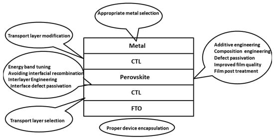
Figure 7. Various strategies to improve stability and avoid degradation in PSCs.
Composition engineering is an effective approach for the stability and performance enhancement of the PSCs [119]. In this strategy, the anion and/or cation of the perovskite material with crystal structure ABX3 is substituted either partially or totally with a desirable material improving the optoelectronic property of the device. In the perovskite material MAPbI3, the conduction band minima are directed by the p-orbital of Pb. The valance band maxima are directed by s and p orbital of Pb and p-orbital of I. The A-site of the perovskite structure does not contribute to the band edge but contributes to the deep energy level of the material. Studies suggest that on tuning A-site the optoelectronic properties of the material can be easily tuned [120]. These modifications also improve other factors, such as thermal stability. The substitution of FA in place of MA at A-site, leads to a stronger bond formation with PbX6 octahedra due to the presence of a larger number of H-bonds. This not only modifies the optoelectronic property of the material but also enhances the thermal stability [121]. The substitution of an inorganic cation such as Cs in place of MA has proved to form stronger bonds as compared to H-bonds. Similarly, mixed halide perovskites have exhibited better stability and efficiency [122]. The partial substitution of X-site I by other halides is another strategy of composition engineering. The substitution of I by Br and Cl increases bandgap and reduces the device efficiency. Therefore, limited substitution has to be done such that efficiency is not much reduced and better stability is attained [123]. Apart from the basic components, the addition of certain materials as an additive has the capability to enhance the performance of the PSC. Several studies have been conducted and certain materials are proven beneficial for the PSCs. Additives can be classified into two categories: (i) additives with precursor of one-step method; (ii) additives with organic solvent at two-step solution method, and additives with antisolvents. This is a broad research field and several reviews based on it can be easily obtained from the literature [124]. The material used along with the quality of the charge transport layer (CTL) affects the performance of the PSCs. The material for the electron transport layer (ETL) must be selected such that the conduction band edge is either equal to or lower than the conduction band of perovskite material, such that the photogenerated electrons from the perovskite layer can be easily received. The valance band of the ETL must lie below the perovskite layer, such that the generated holes can be blocked [125,126]. Similarly, the material for the hole transport layer (HTL) must be selected such that the valance band maxima of the material must be in the proper position to receive the photogenerated holes and the conduction band must be at a high position to stop the photogenerated electrons. In order to attain higher efficiency, proper band alignment between the perovskite layer and CTLs must be done. Energy band tuning is the sole field of the study conducted in the PSCs to attain the best possible performance [127]. The proper energy band tuning ensures minimal interfacial recombination [128]. Apart from proper band alignment of the CTL other properties such as thermal stability, chemical reactivity, etc. impact the performance of the cell to a great extent. Defect passivation is another important strategy to overcome the issue of stability. Certain defect passivation techniques such as interlayer engineering, perovskite film formation conditions, film post-treatment, grain boundary passivation and more are being used by the researchers. The intrinsic stability of the perovskite film is attributed to the crystallographic and molecular structure of the material. The lattice imperfections within the material are dependent on stoichiometry, annealing time, annealing temperature, film deposition method, deposition time, and more [129]. The existence of the defects is determined by the defect formation energy of the material. All the above-stated conditions decide the defect formation energy of the material. Apart from the synthesis conditions, external factors such as moisture, heat, temperature, oxygen, etc. lead to the formation of the new defects during the operation of the PSCs, which in turn has a degrading impact [130]. This rapid degradation of the PSCs has hampered the commercialization of the PSCs despite attaining good performance.
3. Commercialization of PSCs
Long-term device stability is a vital parameter to determine the commercialization of PSCs. The device stability is evaluated in terms of device lifetime tested under 1-sun illumination at electric load. However, PSCs have not attained stability comparable to Si PVs because of their van der Waals interaction causing ion immigration, photo-degradation and phase segregation. Further, the poor intrinsic stability and soft ion lattice due to weak H-bond lead to poor stability.
The various commercialization companies are Oxford PV GmbH (Brandenburg, Germany), Swift solar (Sancarlos, CA, USA), Solaronix (Aubonne, Switzerland), Saule Technology (Wroclaw, Poland), Microquanta Semiconductor (Hangzhou, China) etc. [131]. Oxford PV developed the world’s first full-size 100MW production line [132]. Many commercial companies in China and other countries are working on industrialization of PSCs such as GCL perovskites, Microquanta and a few more. Table 3 summarizes the details of the large-scale PSC modules. One potential issue for perovskite solar cells is the scalability needed for commercialization. The spin-coating method used for the majority of laboratory-scale tests is not effective for producing large-scale uniform coatings. This is because of the lack of consistency in film thickness over a large area, large material waste and lack of compatibility with the roll-to-roll processing that has a high throughput [133,134]. Industrial-scale techniques such as screen printing and slot-die coating have been identified as the most promising solutions to this [135]. They have already been used successfully to fabricate modules over 100 cm2.
Table 3. Details of large-scale PSC modules fabricated by various companies or institutions.
| Company/Institution Name | Country | PCE | Details | Module Area | Reference |
|---|---|---|---|---|---|
| Oxford Photovoltaics |
United Kingdom |
29.52% | Silicon-perovskite bifacial tandem cell | 1 cm2 per cell | [136] |
| Kaunas University of Technology | Lithuania | 23.9% | Using spin coating | 26 cm2 active area of module | [137] |
| Saule Technology | Poland | 10.2% | Doctor blade coating | 15.7 cm2 flexible module | [138] |
| Imec | Belgium | 18.6% | Perovskite solar cell | 16 cm2 module | [139] |
| NEDO and Panasonic |
Japan | 16.09% | Using inkjet printing | 802 cm2 module | [140] |
| Toshiba and NEDO | Japan | 11.7% | Perovskite solar cell (adjusting crystal growth) | 703 cm2 module | [141] |
| Solliance | Netherland | 14.5% | Using the slot die coating | 144 cm2 per cell | [142] |
| Chinese Academy of Science (CAS) | China | 19.2% | Using the slot die coating | 16 cm2 module | [143] |
| Microquanta | China | 24.1% | Perovskite solar cell | 20 cm2 module | [144] |
4. Future Outlook
For more than half a century, silicon PV technology dominates the largest PV market. Studies suggest that in order to obtain the highest efficiency from tandem cells, a wide bandgap perovskite material of bandgap of order 1.7 eV with a thickness of the order of 1 µm must be used. The synthesis of such perovskite material is a hot topic of research among the researchers of the PV community. If a perovskite material of bandgap 1.7 eV is obtained, then extracted voltage will reach about 1.3 V rendering the overall voltage of the device to be 2.0 V. In order to extract similar currents from both the cells, the thickness of the perovskite material must be of order 1 µm with a bandgap of about 1.7 eV. However, preparing high-quality microns-thick perovskite material is still a challenge. Another way to enhance the efficiency of the solar cells is to modify the tunnel junction material [145]. The widely used transparent conductive oxide (TCO) is indium tin oxide (ITO). ITOs are not considered ideal due to their improper transmissivity. The ITOs exhibit parasitic absorption at a range of 800 nm [146]. An ideal tunnelling junction must have high conductance and high transmittance in order to minimize recombination loss. An appropriate refractive index and thickness are also important to minimize the anisotropic conductance, and internal reflection and avoid lateral breakdown. It can be said that industrialization of tandem cells is completely dependent upon the development of perovskite materials.
Currently, state-of-the-art perovskite solar cells still require the use of lead (Pb2+) as the B-cation site. Lead is a toxic element and its use could present problems if released into the environment, eventually working its way into the human food chain [147]. Therefore, a large amount of research has been conducted into alternative lead-free perovskite materials. Perovskite solar cells based on different elements such as antimony, copper, germanium, bismuth and others have all been tested [148,149,150,151,152]. The strongest candidate appears to be tin, having both a similar ionic radius and electronic configuration. This allows direct replacement of the lead ion in the B-site without a significant phase change. Tin-based perovskite cells have a PCE of around 10–12%, which is significantly lower than lead-containing perovskites [153,154]. It is also important to make sure that environmental burden-shifting is not taking place, as studies have found the oxidation of Sn2+ to Sn4+ can lead to the formation of toxic by-product hydroiodic acid [155]. Overall, Ju et al. state that only once the degradation and toxicity mechanisms of current perovskites are understood will lead-free, stable perovskites be fabricated [156]. Single-junction perovskite solar cells are not the only technology that has seen a large jump in PCE over the previous decade. Tandem solar cells involving perovskite have been developed and are not constrained to the single-junction Shockley–Quessier limit. The efficiency limit for a tandem solar cell is 47%, much higher than the 31% for single-junction [157,158]. This is possible as Tandem solar cells better utilize small wavelength radiation from the spectrum. The tandem cell will have a top layer with a large bandgap material; this will absorb the short wavelength part of the spectrum. The longer wavelength radiation will pass through the top layer and be absorbed by the smaller band-gap bottom layer [159]. Perovskites can be combined with a variety of materials to create two-terminal tandem cells. Perovskite-Silicon has shown good performance reaching a PCE of 29.15%, outperforming the highest achieving monocrystalline silicon cell [160]. Perovskite–Perovskite cells have reached an impressive PCE of 24.8% [161]. Another successful combination of materials is perovskite with second-generation material CIGS, achieving 24.2% [162]. Overall, the high theoretical efficiency of tandem perovskite solar cells is predicted to allow the price of PV to continue to fall over the coming decades [163].
Two-dimensional (2D) Perovskites have also been explored as light absorbers for solar cells due to their wide structural diversity and superior stability compared to conventional 3D perovskites [164]. 2D perovskites are produced by using larger ammonium or diammonium cations. These cations are too large and divide the perovskite structure into 2D layers. The layered structures are placed into several categories, with Ruddlesden–Popper (RP) and Dion–Jacobson (DJ) being by far the most common [165,166,167,168]. RP structures are stacked so that they have two offset layers per unit cell having pairs of monovalent interlayer spacer cations. DJ structures can be stacked directly on top of each other and only require one divalent interlayer spacer per formula unit [169]. A successful example of a RP 2D-perovskite (PEA)2(MA)2[Pb3I10] was synthesized and showed excellent resistance to moisture and allowed high-quality films to be produced after just 1-step [170,171]. However, this material only achieved a PCE of 4.73% [172]. Further improvement of the efficiency was made by improving the charge transport mechanism, reaching a PCE of 12.52% [173]. Although, 2D-perovskites show excellent stability they still lack the efficiency of 3D-perovskite cells. For this reason, they are not suitable for single-junction cells but may be an excellent option for use as the high band-gap absorber in a tandem cell [174]. The applications of perovskite material in PV involve usage in electric vehicles and building integrated technology because of its flexibility and tunable bandgap [175,176]. The increment in stability and performance enables the researchers to work not only on performance enhancement but to seek new applications as well. The proper surface engineering and interface engineering improved the efficiency and stability to a great extent. The performance improvement occurred due to a reduction in defect density within the material leading to a decrement in non-radiative recombination. The performance of PSCs is further improved by the surface passivation using hydrophobic molecules. Liang et al. used organic hydrophobic molecules (Benzylamine) with a side chain to enhance the performance of Formamidinium lead iodide (FAPbI3) films. This modification not only enhanced the voltage from 1 to 1.12 V but the stability improved from three days to four months [177,178]. It can be said that depositing high-quality perovskite film with minimum defects can enhance the performance of the PSCs.
Building integration of perovskite-based PV is probably one of the promising approaches. Building energy currently consumes significant energy which must be reduced by employing an energy-positive building envelope [179,180,181,182,183]. For decades, PV technology is placed in a building in terms of roof integrated or wall integrated technology. These are mainly known as building attached or applied PV. Building integrated type PV application semitransparent PV is a precondition [184,185]. However, previously most investigation was devoted based on first-generation silicon [186,187,188] or second-generation thin film-based PV [189,190,191]. However, the booming Perovskite industry gives high hope for the building industry [192,193]. Perovskite which can have variable [194] or static [195] transparency is the most suitable for building window or façade applications. The recent trend is to include a smart switchable or adaptive window in a building [196,197,198,199,200,201,202,203]. However, these most effective windows can only reduce energy consumption [204,205,206,207,208]. In the future, switchable perovskite can be a dominant player in the building industry which can have the potential to generate benign electricity and also tune the transparency concomitantly.
This entry is adapted from the peer-reviewed paper 10.3390/coatings12081089
This entry is offline, you can click here to edit this entry!