Your browser does not fully support modern features. Please upgrade for a smoother experience.
Please note this is an old version of this entry, which may differ significantly from the current revision.
Subjects:
Computer Science, Cybernetics
Optical information processing is introduced and established by utilizing all of light’s attributes of speed and parallelism to handle data at a high rate. The data are represented as a light wave or graphic. The inherent parallel processing of OC was frequently noted as a fundamental benefit of optical processing over electronic processing employing predominantly serial processors.
- optical computing
- logic gates
- neural networks
1. Introduction
The topic of optical computing (OC) dates to the early 1960s, or perhaps before when the military became interested in utilizing the Fourier transform (FT) relationships essential in coherent optical imaging systems to perform processes such as convolution and correlation. On data supplied in imaging the optical format to a bulk optical system, it was easily demonstrated that these processes could be performed with considerable speed. Such processors were fundamentally analog in operation, and as a result, they constantly struggled to maintain adequate dynamic range and signal-to-noise ratios, severely restricting their use. Despite several spectacular demonstrations, silicon digital electronic processing appears to have nearly always been chosen for final manufacturing equipment [1]. Nonetheless, there is still a lot of interest in such specialized machines, and it is certainly true that they can attain very high comparable digital processing speeds. The use of nonlinear optical tools to establish the basic digital processing functions of AND, OR, NAND, NOR, etc., sparked even more interest in the early 1980s, this time in imaging optical format, where a single lens could, in theory, image a very large number of parallel channels from a 2D array of devices. As a result, assertions have been made that those future high-speed computers would use vastly parallel digital–optical processing to attain speeds much above those conceivable with electronics [2].
Following that, a slew of large R&D initiatives aimed at capitalizing on the potential. Such statements are established on basic expectations about prospective digital throughput, but they easily disregard the enormous practical issues that come with putting them into practice. Because the analog light wave level represents the digital state, practically all-optical logic systems addressed in the literature use threshold logic, meaning highly tight control of the optical power level across a complicated multichannel system. Given how readily unanticipated 3 dB insertion losses may be obtained in complicated systems of mirrors, holograms, lenses, and other components, one would wonder if this had any chance of being realized. Nevertheless, employing a dual-rail optical signaling system, the symmetric self-electrooptic effect device (SEED) technique established at AT&T Bell Labs and explored elsewhere does give a sophisticated resolution to this problem [3]. Other important concerns include the fact that the finest optical logic systems are optically activated electrical equipment, and huge ones at that because light must enter them, and optical wavelengths are extremely long by electronic norms. The practical concerns of compiling high-resolution imaging optical systems, the shallow depth of field, the accuracy inferred in the lenses (in terms of focal length), and the mechanical tolerances and massive dimensions of constructed structures are all simple issues that are conveniently overlooked by many. Nevertheless, none of these disadvantages indicates that it cannot be achieved; rather, they raise the challenge, and as some of the results will demonstrate, genuinely spectacular experimental procedures established on free-space optics may be created in the research laboratory.
The switches, optical logic gates (OLGs), and memory components that regulate the flow of electrons in an electronic computer would be replaced by optical systems in a digital optical computer. Optical modulators, which come in a variety of shapes and sizes, may perform the roles of the OLGs and switches. A 1 × 1 switch is a simple on–off switch with the ability to link two lines. A 1 × 2 switch connects one line to one of two lines. Two lines are connected by a 2 × 2 switch. It can be in one of two states: input (I/P) 1 linked to output (O/P) 1 and I/P 2 connected to O/P 2, or I/P 1 connected to O/P 2 and I/P 2 connected to O/P 1, which is known as the bar state, or I/P 1 connected to O/P 2 and I/P 2 connected to O/P 1, which is known as the cross-state. As a result, it is known as a crossbar switch. A crossbar switch may be stretched to n × n arrangement, which allows any of n I/P lines to be linked to any of n O/P lines at any time without causing interference.
Optical switches can be made from electro-optic modulators, acousto-optic modulators, magneto-optic modulators, and liquid crystals, among other forms of optical modulators. A crossbar switch can also be made from an array of modulators. An array of n × n light valves, for instance, might be used to create an n × n crossbar switch. The light source would be a vertical linear array of n laser diodes. The light from the diodes is dispersed horizontally by a cylindrical lens such that each diode illumines one row of the n × n array. Then, one lens per row of the modulator array, a set of n cylindrical lenses, positioned perpendicular to the first lens, is employed to direct the signal emitted by the array onto a horizontally oriented linear array of n photodetectors. This setup allows light from any laser diode to be connected to any detector without interruption. Switches that are operated both electrically and optically have been designed. Optically regulated apparatuses would be used in an all-optical computer. The switches should also be tiny, high-speed apparatuses that can be produced in vast arrays and consume very little switching energy. Several alternative technologies have been used to illustrate the needed switching functionalities. However, massive, high-density arrays of OLGs are currently being developed.
A multinational research team led by Russia’s Skolkovo Institute of Science and Technology has developed an exceptionally energy-efficient optical switch in conjunction with IBM [4]. The switch is extremely rapid and does not involve any cooling. It might serve as the foundation for the next generation of computers that manage photons instead of electrons. A 35-nanometer semi-conducting polymer consisting of organic material is placed between highly reflecting surfaces to form the switch. This results in the formation of a tiny chamber that traps light beams. The gadget is powered by two lasers: a pump laser and a seed laser. When the pump laser shines on the switch, thousands of indistinguishable quasiparticles develop in the same area, generating a Bose–Einstein condensate—a collection of particles that individually act like a single atom. The seed beam is utilized to alter this condensate between two measured states that act as binary codes ‘0′ and ‘1′. The new technology can do 1 trillion calculations per second, which is 1000 times quicker than today’s finest commercial transistors. Furthermore, it requires significantly less energy to transition states than transistors. This is due to the optical switch’s ability to be actuated by a single photon of light. Equivalent electrical transistors that employ single electrons typically need enormous quantities of a cooling device that uses a lot of electricity. The new switch, on the other hand, will function at room temperature. Before it can be deployed, the technology has a long way to go. The first electronic transistor takes years to make its way into a personal computer. The researchers face a hurdle in that, despite requiring relatively little energy to switch, the device still requires continual input from the pump laser. The team is researching ways to get around this by employing superfluorescent perovskite supercrystals to aid reduce power usage. Despite the difficulties, the researchers expect that the novel switch will be employed in various types of optical computing systems in the near future, maybe as a method to ramp up supercomputer processing [4].
The urgent demand for optical technology relies on the fact that the time response of electrical circuits limits today’s computers [5]. A solid transmission medium restricts signal speed and volume while also generating heat that destroys components. A one-foot length of wire, for instance, creates roughly one nanosecond (billionth of a second) of time delay. The extreme downsizing of microscopic electronic apparatuses also causes ‘cross-talk’ or signal mistakes that compromise the system’s dependability. These and other challenges have prompted researchers to look for solutions in light itself. Light does not even have the time domain restrictions of electronics, does not require insulators, and may even deliver dozens or hundreds of photon communication streams at distinct color frequencies at the same time. Those that are not susceptible to EM interference do not experience electrical short circuits. They feature low-loss transmission and a broad bandwidth; that is, they can communicate with numerous channels simultaneously without interference. They may transmit signals inside the same or neighboring optical fibers (OFs) with little to no interference or cross-talk. They are smaller, lighter, and less costly to produce, and they work better with stored data than magnetic materials. Scientists want to construct a new class of computers that run 100 million times quicker than today’s apparatuses by restoring electrons and cables with photons, OF, crystals, thin films, and mirrors [6].
Optical processing hits at a critical juncture in computing history. The need for artificial intelligence (AI) is growing at the same time as Moore’s Law is breaking down in silicon-based computing. Optalysys is a game-changing technology startup that uses groundbreaking optical processing techniques to address this challenge, allowing new levels of AI capability for high-resolution image and video-based applications [7]. The technology is emerging to speed up several of the most demanding processor-intensive operations while using a fraction of the energy that silicon processors consume. It may be configured to execute optical correlation and convolution operations using the application programming interface (API) or Tensorflow interface to unleash new levels of AI and pattern recognition potential. Optalysys employs photons instead of electrons, but it also uses high-resolution computations, allowing huge image/pattern-based data to be handled at speeds significantly quicker than silicon. The Optalysys technology can deliver something distinctive in the API space: a scalable processor that can accomplish end-to-end, full-resolution processing of multi-megapixel image and video data, or contextually pre-process data for enhancing the effectiveness of existing Convolutional Neural Network (CNN)-type models for high-resolution data applications, thanks to the characteristics of diffractive optics.
2. Types of Computing and Necessity of Optics for Computing
OC may be divided into two types: digital optical computing (DOC) and analog optical computing (AOC). For more than 30 years, DOC established on Boolean logics has been established, employing a technique comparable to general-purpose computing established on transistors. Nonetheless, given reduced optical device integration density, it is impossible to beat traditional digital computing. AOC, on the other hand, makes use of the physical characteristics of light, including amplitude and phase, as well as the interactions between light and optical apparatuses, to perform specific computations. Due to the obvious unique mathematical portrayal of computational processes in one AOC system, it is considered dedicated computing. AOC can achieve higher data processing speed in specialized applications, including pattern recognition and numerical calculation, as compared to standard digital computing. As a result, AOC systems have received a lot of academic attention as one of the most potential pervasive computing in the post-Moore age.
Optical technology offers tremendous improvements in computational efficiency and speed along with considerable size and cost reductions [8,9]. Since many processes may be conducted at the same time, an optical desktop computer might process data 100,000 times quicker than existing versions. Low production costs, resilience to electromagnetic (EM) interference, low-loss transmission tolerance, independence from short electrical connections, and the capacity to deliver wide bandwidth and transport signals without interference within the same or neighboring OFs are all features of optics. The distinction between optical and electrical synchrony may be shown with a simplistic example. Imagine an imaging system with 1000 × 1000 distinct units per mm2 in the object plane that are optically coupled to a comparable number of points per mm2 in the image plane; the lens essentially conducts a real-time fast fourier transform (FFT) of the image plane. A million processes are necessary to do this electronically. If parallelism is combined with rapid switching speeds, startling computing speeds are possible. Consider there are only 100 million OLGs on a chip, which is significantly fewer than the figure indicated above. Furthermore, imagine that each OLG has a switching period of just 1 nanosecond (organic optical switches may switch at sub-picosecond rates, but electronic switching has a maximum picosecond switching time). Well over 1017-bit operations per second may be performed by such a device. When compared to the gigabits (109) or terabits (1012) per second speeds that electronics are now restricted to or aiming for, this is a significant difference. In other words, an operation that would take a normal computer a hundred thousand hours (>11 years) might just be completed in less than an hour by an optical computer.
As photons are uncharged and do not react with each other as easily as electrons, light does have another benefit. As a result, in full-duplex functioning, beams of light can travel across each other without altering the information transmitted. Loops in electronics produce noisy voltage spikes anytime the EM fields pass through the loop change. Furthermore, switching pulses with a high frequency or a short duration will generate crosstalk in surrounding lines. Signals in nearby OFs or optical integrated channels are unaffected by each other, and they do not pick up noise from loops. Ultimately, optical materials outperform magnetic materials in terms of storage density and availability. The subject of OC is growing quickly and offers many exciting possibilities for transcending the limits of today’s electrical computers. Optical apparatuses are already being integrated into a variety of computing systems. Resulting in mass manufacture, the cost of laser diodes as coherent light sources has reduced dramatically. Optical CD-ROM discs have also been widely used in both home and office PCs [10].
3. Optical Processing Architecture
Optical information processing is introduced and established by utilizing all of light’s attributes of speed and parallelism to handle data at a high rate. The data are represented as a light wave or graphic. The inherent parallel processing of OC was frequently noted as a fundamental benefit of optical processing over electronic processing employing predominantly serial processors. As a result, optics hold significant promise for interpreting enormous amounts of data in real time. OC is established on the FT feature of a lens. When employing coherent light, a lens executes the FT of a 2D transparency in its front focal plane in its rear focal plane. The lens computes the precise FT with amplitude and phase in an analog method [11].
The I/P plane, the processing plane, and the O/P plane are the three planes that make up the system. The I/P plane displays the data to be processed; this plane will usually implement an algorithm. Conversion from electricity to light is performed via a Spatial Light Modulator (SLM). A 1D or 2D signal can be used as an I/P. In the context of a 1D I/P signal, an acousto-optic cell is commonly utilized, whereas 2D SLMs are used for 2D signals. Due to the lack of SLMs in the early years, the I/P plane consisted of a stationary slide. As a result, the concepts and possibilities of optical processors could be proved, but no real-time applications could be presented, rendering the processor worthless for most real-world applications. Lenses, holograms (optically recorded or computer produced), and nonlinear components can all be found in the processing plane. This is perhaps the most important component of the processing, and it can be performed at the speed of light in most optical processors. The O/P plane, which detects the processing results, is made up of a photodetector, a photodetector array, or a camera. Since the bulk of them are running at video rates, the speed of the entire process is restricted by the speed of its slowest component, which is usually the I/P plane SLM. The SLM is an essential component in the creation of realistic optical processors, but it is also one of their weakest. Likewise, the poor performance and expensive price of SLMs have slowed the development of a real-time optical processor.
Real-time pattern recognition was first thought to be one of the most potential technologies of optical computers; hence, the following two optical correlator designs were developed. Because the separation between the I/P plane and the O/P plane is four times the focal length of the lenses, the basic correlator is termed 4-f in Figure 1a. This extremely simple design is established on Marechal and Croce’s spatial filtering work in 1953 [12] and was further refined by numerous researchers over the years [13,14]. The I/P scene is projected in the I/P plane, and Lens 1 performs the FT. The reference’s actual conjugated FT is placed in the Fourier plane and hence multiplied by the I/P scene’s FT. Lens 2 uses a second FT to determine the relationship between the I/P scene and the reference in the O/P plane. The fundamental issue of this arrangement was developing a sophisticated filter using the reference’s FT, and Vander Lugt suggested in 1964 to utilize a Fourier hologram of the benchmark as a filter [15]. Figure 1b,c depict the O/P correlation peak for autocorrelation when the correlation filter is a matched filter and when the correlation filter is phase-only, respectively.
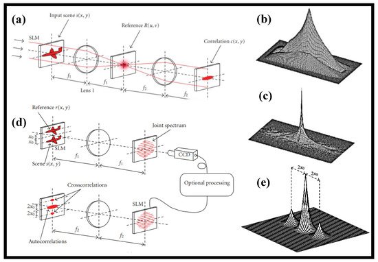
Weaver and Goodman [16] proposed a new optical correlator layout in 1966, the joint transform correlator (JTC), which is shown in Figure 1d. The two pictures, the reference r(x,y) and the scene s(x,y), are arranged beside each other on the I/P plane, which is the first lens FTs. After detecting the intensity of the combined spectrum, the FT is used. The cross-correlations between the scene and the reference are among the terms that make up the second FT. This FT may be completed optically using an SLM, as seen in Figure 1d. When the reference and scene are similar, the O/P plane of the JTC is shown in Figure 1e. The two cross-correlation peaks are the only ones worth looking at. The CCD camera can be exchanged with an optical component such as an optically addressed SLM or a photorefractive crystal to create a completely optical processor. Because the JTC does not need the computation of a correlation filter, it is the appropriate design for real-time applications including target tracking where the benchmark must be revised at a rapid rate. Coherent optical processors are illustrated in Figure 1. Wave intensities, rather than complex wave amplitudes, are used to carry information in incoherent optical processors. Incoherent processors are not affected by phase changes in the I/P plane and do not produce coherent noise. The non-negative real value of the information, on the other hand, necessitates the employment of a variety of methods to execute some image processing applications [17,18]. Linear optical processing may be broken down into space-invariant activities such as correlation and convolution as well as space-variant operations such as coordinate transformations [19] and the Hough transform [20]. Logarithm transformation, thresholding and analog-to-digital conversion are examples of nonlinear processing that may be performed optically [21].
This entry is adapted from the peer-reviewed paper 10.3390/nano12132171
This entry is offline, you can click here to edit this entry!