Ion-Movement-Based Synaptic Device for Brain-Inspired Computing: History
Please note this is an old version of this entry, which may differ significantly from the current revision.
Contributor: ,

As the amount of data has grown exponentially with the advent of artificial intelligence and the Internet of Things, computing systems with high energy efficiency, high scalability, and high processing speed are urgently required. Unlike traditional digital computing, which suffers from the von Neumann bottleneck, brain-inspired computing can provide efficient, parallel, and low-power computation based on analog changes in synaptic connections between neurons. Synapse nodes in brain-inspired computing have been typically implemented with dozens of silicon transistors, which is an energy-intensive and non-scalable approach. Ion-movement-based synaptic devices for brain-inspired computing have attracted increasing attention for mimicking the performance of the biological synapse in the human brain due to their low area and low energy costs.

  • ion movement
  • synaptic device
  • brain-inspired computing

1. Introduction

Explosively increasing data set sizes in artificial intelligence (AI) and the Internet of Things have resulted in us facing limitations in energy efficiency and the challenges of the von Neumann bottleneck approaching the end of Moore’s law [1][2][3][4][5]. In more detail, the AI algorithm that runs on the complementary metal oxide semiconductor (CMOS)-based von Neumann hardware seems to be somewhat inefficient [6], since: (1) the separation of processor and memory causes heavy data traffic between devices, especially in data-intensive tasks; (2) CMOS uses a “0” and “1” binary logic system rather than a gradual weight change; (3) the connections of transistors in silicon chips are usually in two dimensions; (4) CMOS-based computers consume a thousand times as much energy as the human brain to perform the same task [6][7]. For example, a supercomputer (IBM Watson) [8] has 2880 computing cores (10 refrigerators’ worth in size and space) and requires about 80 kW of power and 20 tons of air-conditioned cooling capacity, while the human brain occupies a space of less than 2 l and consumes low power, of the order of 10 W [9][10]. Additionally, if data storage and communication continue to increase at the current rate, the total energy consumed by binary operations using CMOS will reach ~1027 J in 2040, surpassing the total energy produced worldwide [11][12]. In order to improve the performance of computing systems in the so-called “big data” era [13], it is necessary to fundamentally change the way computing is executed [14]. People need to shift to a data-centric paradigm rather than a computer-centric one [14].
The growth of computational power, the availability of big data, and the rapid development of training methods have resulted in significant advances in data-centric computing methods, such as the artificial neural network (ANN), which is inspired by the co-location of logic and memory, tolerance to local failures, hyper-connectivity, and parallel processing present in the human brain [12][15][16]. The human brain is a massively parallel computing structure that processes input information by synaptic transmission. Each synaptic event consumes only around 1–10 fJ [5][17]. The hardware in brain-inspired computing architecture is required to mimic stochastic behaviors by introducing a new logic device such as an orthogonator gate and to physically emulate synapses in the human brain at the small circuit or device levels, consuming significantly reduced energy [12][18][19][20][21][22][23][24].
Recently, synaptic devices based on various types of resistive switching devices have been utilized for brain-inspired computing [25][26][27][28][29][30]. Brain-inspired computing based on synaptic devices has achieved particular progress from ion-movement-based resistive switching mechanisms such as cation-movement-based filaments [31][32][33][34][35][36], anion-movement-based filaments [37][38][39][40][41][42][43], cation-movement-based ferroelectric polarization reversal [44][45][46][47][48][49], and ion-movement-based electrochemical electrolytes [50][51][52][53][54][55][56][57]. These ion-movement-based resistive switching devices can show a gradual change in conductance and nonvolatile characteristics, which have not been implemented in Mott-insulator-based resistive switching devices. Resistive switching based on the phase transition of Mott insulators under an electric field shows an abrupt change in conductance and volatile behaviors, which are suitable for neuron devices [58][59][60]. In this entry, researchers summarize in detail the different ion-movement-based mechanisms and discuss the advances in the development of ion-movement-based resistive switching devices for artificial synaptic elements. In addition, researchers discuss the challenges that need to be addressed in future research on synaptic devices towards developing brain-inspired computing systems.

2. Biological Synapses

2.1. Properties of Biological Synapses

The brain contains billions of neurons, which are highly connected by trillions of synapses [6]. Synapses are small gaps (20–40 nm) between the axon end of the presynaptic neuron and the dendrites of the postsynaptic neuron (Figure 1a) [61]. Neurons generate action potentials (spikes) with amplitudes of approximately 100 mV and durations in the range of 0.1–1 ms in their soma. The spikes propagate through the axon and are transmitted to the postsynaptic neurons through the synapses [10]. The connection weights of the synapses between neurons can become stronger (potentiation) or weaker (depression) through a process called synaptic plasticity, as the brain adapts to new information. Synaptic plasticity is widely believed to play a key role in the learning and memory processes of the brain [61].
Figure 1. Properties of a biological synapse. (a) Schematic image of the biological synapse structure. Typical synaptic weight changes in the cases of (b) LTP and LTD, (c) STP and STD, and (d) STDP.

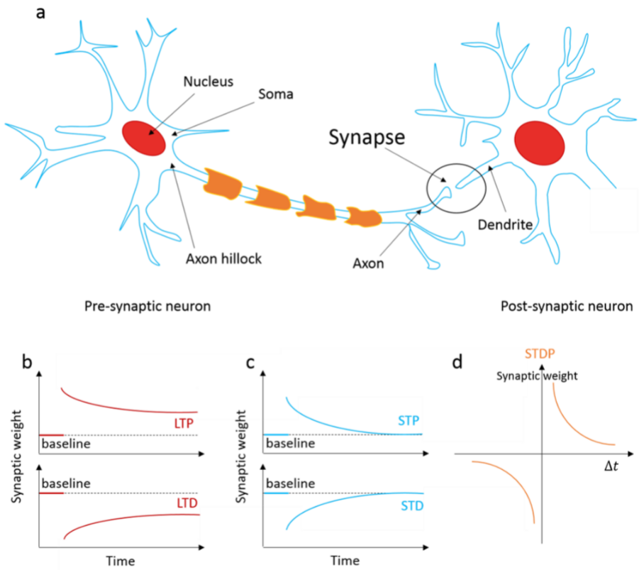
2.2. Biological Synaptic Plasticity

Biological synaptic plasticity, which enables learning and memory, is the ability to continuously modulate synaptic weights in response to action potentials. In more detail, biological synaptic plasticity is the changed connection strength of a biological synapse, which is caused by the activities of a presynaptic neuron and a postsynaptic neuron. [10] It includes long-term potentiation/depression, short-term potentiation/depression, and spike-timing-dependent plasticity (STDP). The biological synaptic weight can be persistently changed by modulating the amount of neurotransmitter presynaptically released across the synapse or the number of receptors present postsynaptically; this is so-called long-term plasticity. Specifically, the increases and decreases in synaptic weight are called long-term potentiation (LTP) and long-term depression (LTD), respectively (Figure 1b) [5][62]. Short-term potentiation (STP) and short-term depression (STD) are temporary increases and decreases in synaptic weight, respectively. STP and STD generally last from seconds to tens of minutes and then fade away to the initial values, in biological systems (Figure 1c) [5][63]. Spike-timing-dependent plasticity (STDP), a form of Hebbian learning, emerged as a new concept of cellular learning in the late 1990s [10][64][65][66]. Different types of STDP exhibit different forms of dependency on the spiking time Δt=tpretpost, where tpre and tpost are the arrival times of presynaptic and postsynaptic spikes, respectively. As the amplitude of Δt becomes shorter, the change in synaptic weight becomes larger (Figure 1d).

3. Synaptic Devices

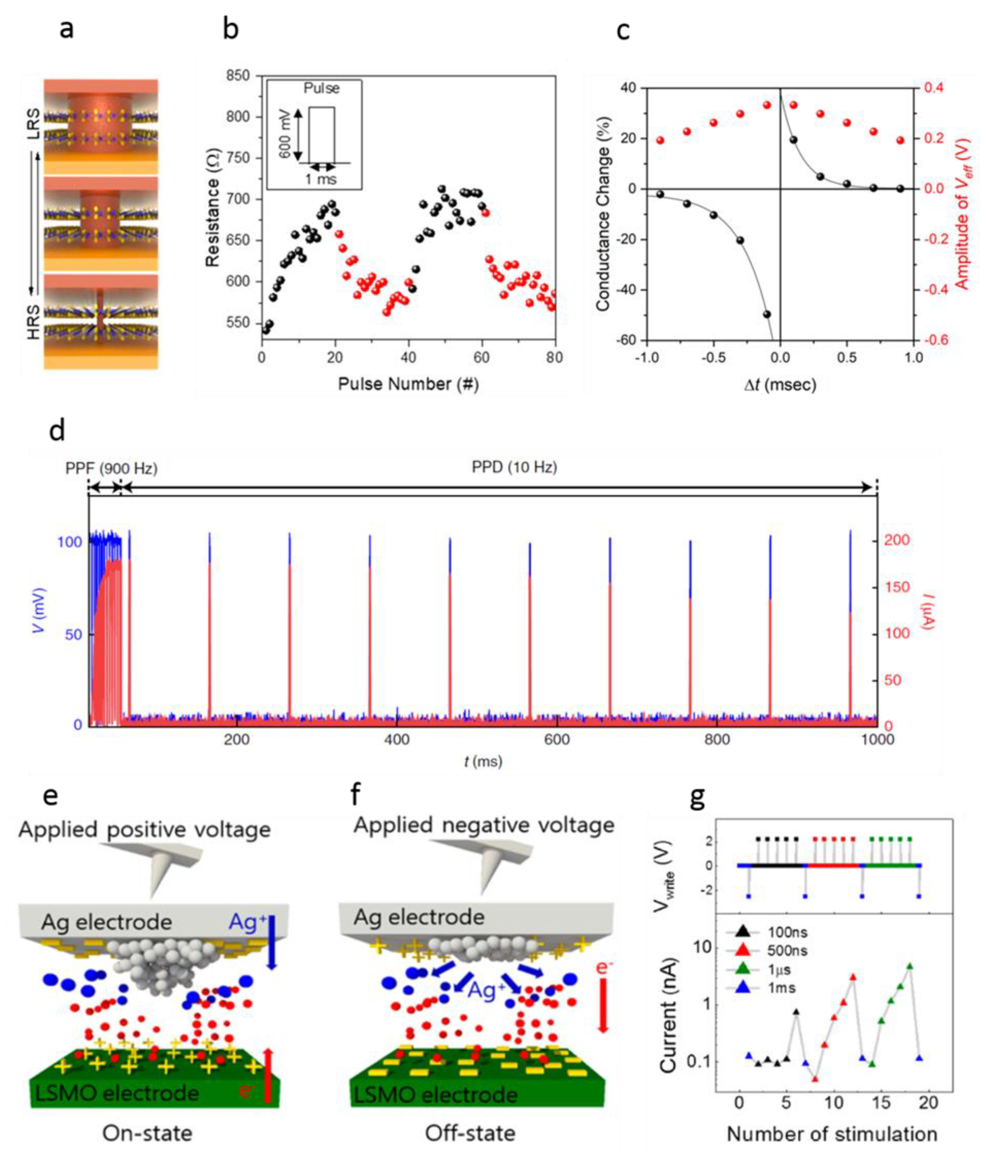
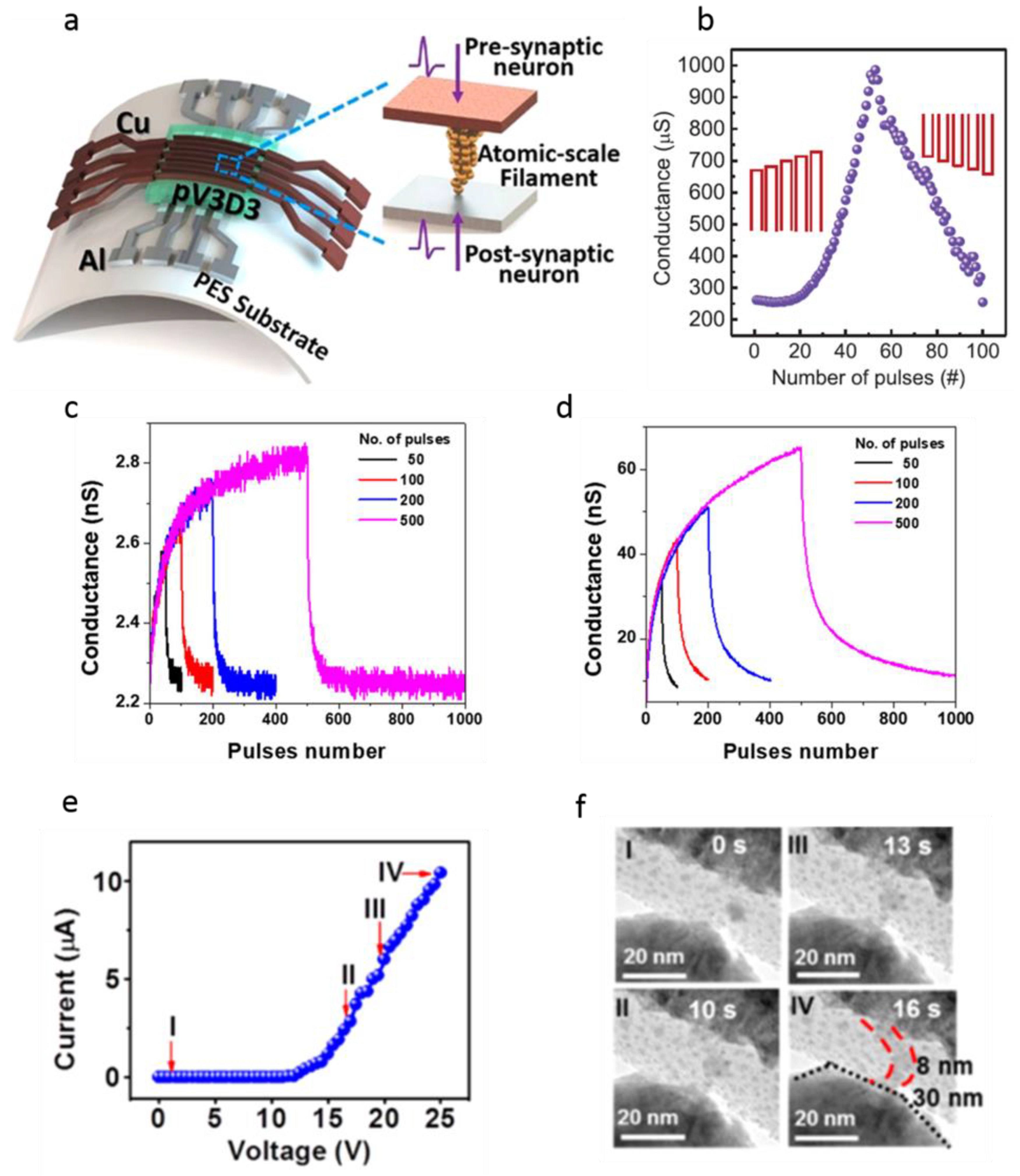
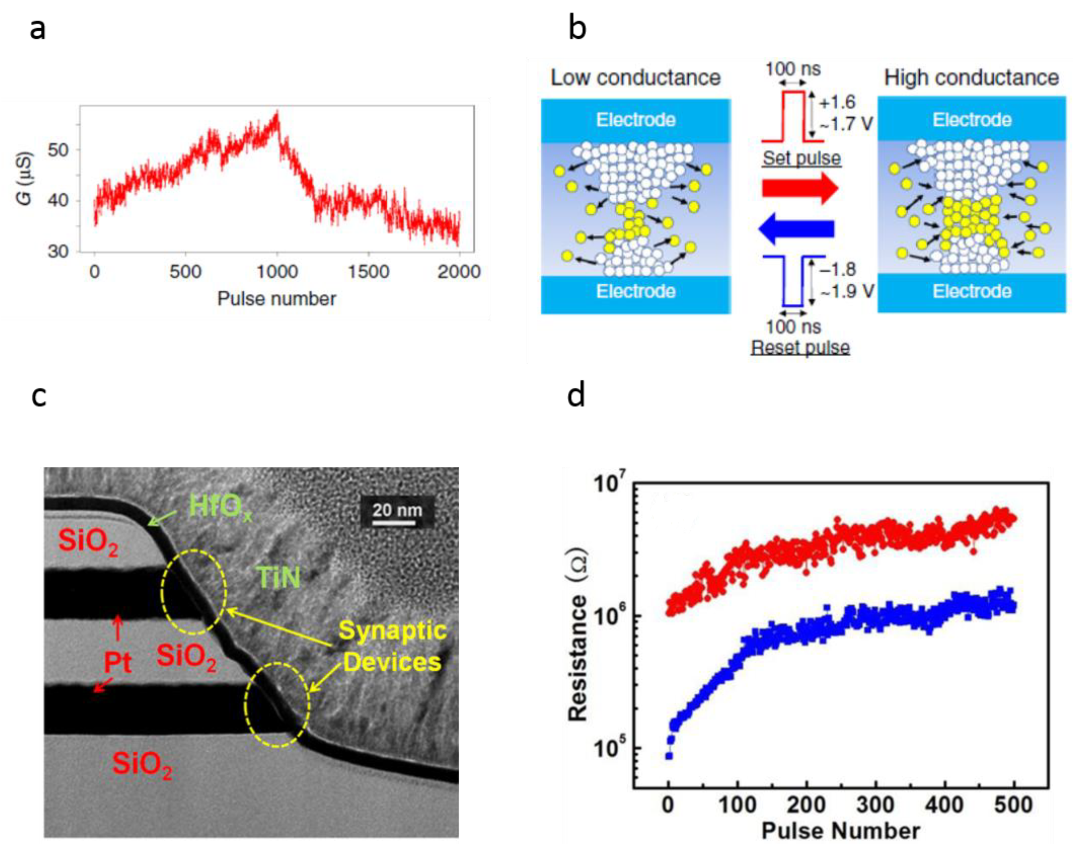
3.1. Cation-Movement-Based Filamentary Two-Terminal Synaptic Devices

To mimic biological synaptic plasticity, it is essential to demonstrate repeatable analog switching with ultra-low power or energy consumption. The attractive characteristics of the ECM cell such as short switching time, scalability, and ultra-low power or energy consumption have driven the development of synaptic devices. To improve the performance of energy-efficient analog switching, emerging electrolytes for ECM cells such as 2D materials, nanowires, polymers, and ultra-thin films have been used [31][32][33][34][67].
The Cu/MoS2 bilayer/Au system has been reported for a synaptic device with ultra-low switching voltage (Figure 2a,b) [31]. In the MoS2 bilayer between an active Cu top electrode and an inert Au bottom electrode, Cu has a lower migration barrier and diffusion activation energy than sulfur vacancies, leading to the operation of the synaptic device at ultra-low switching voltages. A pulse with a small amplitude of 0.6 V can cause a gradual increase and decrease in the device resistance, resulting in potentiation–depression curves (Figure 2b). Such low switching voltages are important, especially for neuromorphic computing, which strives to operate with a power far lower than that required for digital computing [31]. In addition, the STDP of the cation-movement-based filamentary two-terminal synaptic device was experimentally confirmed, as shown in Figure 2c. The developed device reveals consistent analog switching and thus exhibits synapse-like learning behavior such as STDP, which was demonstrated for the first time in 2D-material-based vertical memristors. This demonstration of STDP combined with low switching voltage is promising for applications in neuromorphic circuits.
Figure 2. (a) Schematic of the change in the cation–movement–based filament for the Cu/MoS2 double-layer/Au with switching between HRS and LRS. (b) Potentiation–depression curve obtained by consecutive pulses with a small amplitude of 0.6 V and (c) STDP behaviors obtained by low–amplitude spiking for the Cu/MoS2 double–layer/Au. Reprinted/adapted with permission from Ref. [31]. 2019, American Chemical Society. (d) The current response of frequency–dependent PPF and PPD obtained by input pulses (100 mV, 1 ms) in a cation–movement–based filamentary two–terminal synaptic device with protein nanowires. Reprinted/adapted with permission from Ref. [32]. 2020, Springer Nature. (e,f) Schematic illustrations of growth and rupture of an uncompleted CF of Ag in an Ag/PZT/LSMO device in LRS and HRS, respectively. (g) Potentiation behaviors obtained by stimulation pulses with different durations for an Ag/PZT/LSMO device. Reprinted/adapted with permission from Ref. [33]. 2017, American Chemical Society.
Fu et al. demonstrated a type of diffusive memristor which is fabricated using protein nanowires harvested from the bacterium Geobacter sulfurreducens and operates at biological voltages of 40–100 mV [32]. They demonstrated that a reduction in the switching voltage is obtained by using protein nanowires. The influx and efflux of Ag in the CF can also emulate Ca2+ influx and extrusion in a biological synapse. The steady-state evolution of the CF and the resultant change in conductance can be used to emulate synaptic plasticity. Figure 2d shows frequency-dependent paired-pulse facilitation (PPF) and paired-pulse depression (PPD) in a synaptic device operating at biological voltages. The features of the protein-nanowire-based filamentary devices are very similar to those of biological synapses in terms of signal amplitude and/or frequency range.
It has been reported that a synaptic Ag/PbZr0.52Ti0.48O3 (PZT)/La0.8Sr0.2MnO3 (LSMO) device with an ultra-thin ferroelectric PZT layer (~4 nm) serving as an electrolyte for cation migration can achieve very low energy consumption [33]. The ferroelectric barrier width becomes thinner due to the growth of an uncompleted CF of Ag, leading to a higher tunneling transmittance and switching to a low on-state resistance, as shown in Figure 2e. The rupture of the Ag CF takes place due to a thermally assisted electrochemical reaction (Figure 2f). Then, the tunneling barrier width becomes thicker, and the device switches back to a high off-state resistance. The gradual change in the direct tunneling current of the Ag/PZT/LSMO is enabled by barrier-width control originating from the Ag ion migration. Both potentiation and depression can be induced in the Ag/PZT/LSMO device by short stimulation pulses with a duration of 100 ns, which are enabled by the combination of applied voltage and polarization bound charge, as shown in Figure 2g. This characteristic could result in low programming energy (a potentiation energy consumption of ~22 aJ and a depression energy consumption of ~2.5 pJ) by minimizing the programming time.
Jang et al. demonstrated that the transition of the operation mode in a poly(1,3,5-trivinyl-1,3,5-trimethyl cyclotrisiloxane) (pV3D3)-based flexible memristor from conventional binary switching to synaptic analog switching can be achieved simply by reducing the size of the formed filament [34]. The flexible pV3D3 memristor operates through the formation and rupture of the Cu CF inside the pV3D3, resulting in the LRS and HRS, respectively, as shown in Figure 3a. Potentiation and depression curves can be induced by the conductance updates of the pV3D3 memristor under the application of consecutive pulses, as shown in Figure 3b. Conductance updates with linear behavior are achieved by utilizing pulse trains with increasing amplitude in the range of 2~4 V (−1.2~−1.4 V) with a width of 60 ns (100 ns) for the potentiation (depression) process.
Figure 3. (a) Schematic image of pV3D3-based flexible synaptic device using the formation and rupture of Cu ion-movement-based filament. (b) Potentiation (depression) curve obtained by smart pulse scheme with increasing amplitude in the range of 2~4 V (−1.2~−1.4 V) with a width of 60 ns (100 ns) for a pV3D3-based flexible synaptic device. Reprinted/adapted with permission from Ref. [34]. 2018, American Chemical Society. (c,d) A comparison of potentiation–depression curves of the Ag/SiNx/a-Si/p++ Si-based devices with unimplanted (c) and implanted (d) devices under varying numbers of stimulation pulses of 7.0 (−3.0) V for potentiation (depression). Reprinted/adapted with permission from Ref. [36]. 2020, Springer Nature. (e) Gradual current change and (f) simultaneously obtained transmission electron microscope image of a Cu tip/SiO2/W cell during injection of voltage with increased amplitude. Reprinted/adapted with permission from Ref. [68]. 2017, American Chemical Society.

3.2. Anion-Movement-Based Filamentary Two-Terminal Synaptic Devices

The key advantages of anion-movement-based filamentary two-terminal synaptic devices include the compact structure, the CMOS compatibility, and the capability for hybrid or 3D integration, making them attractive for a broad range of applications including memory, analog devices, and reconfigurable circuits, as well as brain-inspired computing [37][38].
Gong et al. implemented an anion-movement-based filamentary two-terminal synaptic device through a HfO2-based resistive switching device [41]. This device shows analog switching behavior, as shown in Figure 4a. The conductance of the device gradually increases and decreases under 1000 consecutive positive and negative pulses, respectively. The progressive change in conductance in the HfO2-based synaptic device is attributed to the modulation of the oxygen-vacancy-based filament by pulse stimulation. Figure 4b shows a schematic of its operation mechanism. The movement of the oxygen vacancies in response to an electrical signal has a probabilistic nature, which emerges as an inherent randomness in the conductance weight updates, superimposed on the expected signal.
Figure 4. (a) Gradual increase (decrease) in conductance behavior in the HfO2-based resistive switching device induced by 1000 consecutive identical set (reset) pulses. (b) A conceptual schematic of a CF confined in the HfO2-based resistive switching device during switching corresponding to set and reset. Reprinted/adapted with permission from Ref. [41]. 2018, Springer Nature. (c) Cross-sectional TEM image of a 3D vertical structure based on HfOx cells. (d) Synaptic behavior with different initial resistances (~100 kΩ and 1 MΩ) of the HfO2-based 3D vertical synaptic device. In the initial resistance of the 1 MΩ device, the energy consumption decreases below 1 pJ. Reprinted/adapted with permission from Ref. [42]. 2014, American Chemical Society.
Gao et al. developed a synaptic device based on a 3D vertical structure including several parallel oxide-based resistive switching devices on the same nanopillar, for the application of brain-inspired computing with high device density and low energy consumption [42]Figure 4c shows a TEM image of a two-layer resistive switching device which has top and bottom HfOx-based cells on the same pillar. The analog switching behavior is obtained through only a gradual reset process to mimic biological depression. The abrupt set process is considered as positive feedback between the oxygen vacancy generation rate and the temperature/local field strength, while the gradual reset process is considered as negative feedback [37]Figure 4d shows the gradual reset processes of the device, induced from two initial resistance states (~100 kΩ and 1 MΩ) by applying 500 consecutive negative identical pulses. For the case of an initial resistance state of ~1 MΩ, the maximum energy per spike drops to ~0.29 pJ. The reduced energy consumption is mainly attributed to the higher initial resistance of the device.
Yu et al. implemented an anion-movement-based filamentary two-terminal synaptic device with low energy consumption by stacking multiple layers of Pt/HfOx/TiOx/HfOx/TiOx/TiN [37]. The analog switching behavior is obtained through only a gradual reset process to mimic biological depression. The abrupt set process is considered as positive feedback between the oxygen vacancy generation rate and the temperature/local field strength, while the gradual reset process is considered as negative feedback. The gradual reset processes of five different devices were induced from two initial resistance states (~500 Ω and ~20 kΩ) by applying 400 consecutive negative identical pulses. A system-level simulation using these device-level experimental results revealed that the brain-inspired computing system may be robust against synaptic device variation. In addition, the synaptic device operates with very low energy consumption, which decreases from 24 pJ to 0.85 pJ as the initial resistance increases.

3.3. Cation-Movement-Based Ferroelectric Two-Terminal Synaptic Devices

An ultra-thin ferroelectric material can act as a switching layer in cation-movement-based ferroelectric two-terminal resistive switching devices. The attractive advantages of ferroelectric two-terminal resistive switching devices such as fast switching speed and ultra-low power/energy consumption can lead to high performance in the synaptic devices based on them.
Ma et al. reported that a synaptic device with an ultra-short switching time (600 ps) can be implemented by using a Ag/BaTiO3 (~2.4 nm)/Nb:SrTiO3 ferroelectric tunnel junction [47]. The upward and downward ferroelectric polarization directions correspond to the LRS and HRS, respectively. The switching between the two states is bipolar and, interestingly, not abrupt, leading to a broad range of intermediate resistance states. Figure 5a shows the gradual resistance versus voltage pulse behaviors obtained under different negative voltage ranges (−18, −16, −14, and −12 V) with a fixed pulse duration of 600 ps. The ultra-short switching time can be induced by both the high Nb concentration in the Nb:SrTiO3 semiconducting electrode and the low work function of the metal electrode. Figure 5b shows 32 distinct resistive states of the device which can be maintained with no degradation for 104 s. To mimic biological synaptic plasticity, the sub-nanosecond (600 ps)-driven conductance change is measured, as shown in Figure 5c. A gradual change in the conductance similar to biological synaptic plasticity can be induced by increasing the amplitude of the negative or positive voltage pulses.
Figure 5. (a) Resistive switching with gradual change in Ag/BaTiO3 (~ 2.4 nm)/Nb:SrTiO3 ferroelectric tunnel junction under consecutive pulses (writing voltage = –18, –16, –14, and –12 V, fixed pulse duration = 600 ps). (b) Retention characteristics of the Ag/BaTiO3 (~ 2.4 nm)/Nb:SrTiO3 ferroelectric tunnel junction. (c) Analog switching behaviors of an ultra-thin ferroelectric-film-based synaptic device (Ag/BaTiO3 (~ 2.4 nm)/Nb:SrTiO3) under consecutive non-identical pulses with a sub-nanosecond (600 ps) duration. Reprinted/adapted with permission from Ref. [47]. 2020, Springer Nature. (df) STDP curves of different forms in an ultra-thin ferroelectric-film-based synaptic device (Co/BFO/CCMO). The top and bottom panels show presynaptic and postsynaptic spikes and the change in conductance, respectively. Reprinted/adapted with permission from Ref. [45]. 2017, Springer Nature.
Boyn et al. reported that STDP with an operation time of a few hundred ns can be emulated through ferroelectric domain dynamics [45]. To mimic the various types of STDP shown in Figure 5d–f, they applied different pulse waveforms to a synaptic device based on ferroelectric switching. This procedure allows the generation of biologically realistic, accelerated (Figure 5d,e), or artificially designed (Figure 5f) STDP learning curves. In addition, Figure 5d–f show the excellent agreement between the conductance changes predicted using the nucleation-limited model of ferroelectric domains and the measured conductance variations associated with the various types of STDP.
Chanthbouala et al. reported that a ferroelectric synapse with ultra-short switching time (in the 10–200 ns range) can be implemented by using a Co (10 nm)/Au (10 nm)/BaTiO3 (2 nm)/La0.67Sr0.33MnO3 (30 nm) structure [44]. The upward and downward ferroelectric polarization directions correspond to the LRS and HRS, respectively. The switching between the two states is bipolar and, interestingly, not abrupt; a broad range of intermediate resistance states are observed. The nucleation and growth of ferroelectric domains by systematic variation of the pulse can lead to various resistance states, resulting in synaptic plasticity. Synaptic behaviors based on ferroelectric switching are demonstrated by applying consecutive pulses with a fixed amplitude.

This entry is adapted from the peer-reviewed paper 10.3390/nano12101728

References

  1. Atzori, L.; Iera, A.; Morabito, G. The internet of things: A survey. Comput. Netw. 2010, 54, 2787–2805.
  2. Zanella, A.; Bui, N.; Castellani, A.; Vangelista, L.; Zorzi, M. Internet of things for smart cities. IEEE Internet Things J. 2014, 1, 22–32.
  3. Gubbi, J.; Buyya, R.; Marusic, S.; Palaniswami, M. Internet of things (IoT): A vision, architectural elements, and future directions. Future Gener. Comput. Syst. 2013, 29, 1645–1660.
  4. Hu, M.; Graves, C.E.; Li, C.; Li, Y.; Ge, N.; Montgomery, E.; Davila, N.; Jiang, H.; Williams, R.S.; Yang, J.J.; et al. Memristor-based analog computation and neural network classification with a dot product engine. Adv. Mater. 2018, 30, 1705914.
  5. Park, H.L.; Lee, Y.; Kim, N.; Seo, D.G.; Go, G.T.; Lee, T.W. Flexible Neuromorphic Electronics for Computing, Soft Robotics, and Neuroprosthetics. Adv. Mater. 2020, 32, 1903558.
  6. Xu, M.; Mai, X.; Lin, J.; Zhang, W.; Li, Y.; He, Y.; Tong, H.; Hou, X.; Zhou, P.; Miao, X. Recent Advances on Neuromorphic Devices Based on Chalcogenide Phase-Change Materials. Adv. Funct. Mater. 2020, 30, 2003419.
  7. Silver, D.; Schrittwieser, J.; Simonyan, K.; Antonoglou, I.; Huang, A.; Guez, A.; Hubert, T.; Baker, L.; Lai, M.; Bolton, A.; et al. Mastering the game of Go without human knowledge. Nature 2017, 550, 354.
  8. Ferrucci, D.; Brown, E.; Chu-Carroll, J.; Fan, J.; Gondek, D.; Kalyanpur, A.A.; Lally, A.; Murdock, J.W.; Nyberg, E.; Prager, J. Building Watson: An overview of the DeepQA progect. AI Mag. 2010, 31, 59–79.
  9. Rachlin, H. Making IBM’s computer, Watson, human. Behav. Anal. 2012, 35, 1–16.
  10. Kuzum, D.; Yu, S.; Wong, H.P. Synaptic electronics: Materials, devices and applications. Nanotechnology 2013, 24, 382001.
  11. Jeong, D.S.; Kim, K.M.; Kim, S.; Choi, B.J.; Hwang, C.S. Memristors for Energy-Efficient New Computing Paradigms. Adv. Electron. Mater. 2016, 2, 1600090.
  12. Sangwan, V.K.; Hersam, M.C. Neuromorphic nanoelectronic materials. Nat. Nanotechnol. 2020, 15, 517–528.
  13. Zokopoulos, P.C.; Eaton, C.; Deroos, D.; Deutsch, T.; Lapis, G. Understanding Big Data: Analytics for Enterprise Class Hadoop and Streaming Data; McGraw-Hill: New York, NY, USA, 2012.
  14. Upadhyay, N.K.; Jiang, H.; Wang, Z.; Asapu, S.; Xia, Q.; Yang, J.J. Emerging Memory Devices for Neuromorphic Computing. Adv. Mat. Technol. 2019, 4, 1800589.
  15. Goodfellow, I.; Bengio, Y.; Courville, A. Deep Learning; The MIT Press: Cambridge, MA, USA, 2016.
  16. LeCun, Y.; Bengio, Y.; Hinton, G. Deep learning. Nature 2015, 521, 436–444.
  17. Sengupta, B.; Stemmler, M.B. Power consumption during neuronal computation. Proc. IEEE 2014, 102, 738–750.
  18. James, C.D.; Aimone, J.B.; Miner, N.E.; Vineyard, C.M.; Rothganger, F.H.; Carlson, K.D.; Mulder, S.A.; Draelos, T.J.; Faust, A.; Marinella, M.J.; et al. A historical survey of algorithms and hardware architectures for neural-inspired and neuromorphic computing applications. Biol. Insp. Cog. Arch. 2017, 19, 49–64.
  19. Schuman, C.D.; Potok, T.E.; Patton, R.M.; Birdwell, J.D.; Dean, M.E.; Rose, G.S.; Plank, J.S. A survey of neuromorphic computing and neural networks in hardware. arXiv 2017, arXiv:1705.06963.
  20. Bear, M.F.; Connors, B.W.; Paradiso, M.A. Neuroscience: Exploring the Brain; Wolters Kluwer Health: Philadelphia, PA, USA, 2015.
  21. Indiveri, G.; Chicca, E.; Douglas, R.J. Artificial Cognitive systems: From VLSI networks of spiking neurons to neuromorphic cognition. Cogn. Comput. 2009, 1, 119–127.
  22. Indiveri, G.; Linares-Barranco, B.; Hamilton, T.J.; Schaik, A.; Etienne-Cummings, R.; Delbruck, T.; Liu, S.C.; Dudek, P.; Häfliger, P.; Renaud, S.; et al. Neuromorphic silicon neuron circuit. Front. Neurosci. 2011, 5, 73.
  23. Bezrukov, S.M.; Kish, L.B. Deterministic multivalued logic scheme for information processing and routing in the brain. Phys. Lett. A 2009, 375, 2338–2342.
  24. Gingl, Z.; Kish, L.B.; Khatri, S.P. Towards brain-inspired computing. Fluct. Noise Lett. 2010, 9, 403–412.
  25. Chandrasekar, A.; Rakkiyappan, R. Impulsive controller design for exponential synchronization of delayed stochastic memristor-based recurrent neural networks. Neurocomputing 2016, 173, 1348–1355.
  26. Sun, J.; Han, J.; Wang, Y.; Liu, P. Memristor-based neural network circuit of emotion congruent memory with mental fatigue and emotion inhibition. IEEE Trans. Biomed. Circuits Syst. 2021, 15, 606.
  27. Wang, L.; Shen, Y. Design of controller on synchronization of memristor-based neural networks with time-varying delays. Neurocomputing 2015, 147, 372–379.
  28. Sun, J.; Han, J.; Liu, P.; Wang, Y. Memristor-based neural network circuit of pavlov associative memory with dual mode switching. Int. J. Electron. Commun. AEÜ 2021, 129, 153552.
  29. Sun, J.; Han, G.; Zeng, Z.; Wang, Y. Memristor-based neural network circuit of full-function pavlov associative memory with time delay and variable learning rate. IEEE Trans. Cybern. 2020, 50, 2935.
  30. Jo, S.H.; Chang, T.; Ebong, I.; Bhadviya, B.B.; Mazumder, P.; Lu, W. Nanoscale memristor device as synapse in neuromorphic system. Nano Lett. 2010, 10, 1297–1301.
  31. Xu, R.; Jang, H.; Lee, M.H.; Amanov, D.; Cho, Y.; Kim, H.; Park, S.; Shin, H.; Ham, D. Vertical MoS2 Double-Layer Memristor with Electrochemical Metallization as an Atomic-Scale Synapse with Switching Thresholds approaching 100 mV. Nano Lett. 2019, 19, 2411–2417.
  32. Fu, T.; Liu, X.; Gao, H.; Ward, J.E.; Liu, X.; Yin, B.; Wang, Z.; Zhuo, Y.; Walker, D.J.F.; Yang, J.J.; et al. Bioinspired bio-voltage memristors. Nat. Commun. 2020, 11, 1861.
  33. Yoon, C.; Lee, J.H.; Lee, S.; Jeon, J.H.; Jang, J.T.; Kim, D.H.; Kim, Y.H.; Park, B.H. Synaptic plasticity selectively activated by polarization-dependent energy-efficient ion migration in an ultrathin ferroelectric tunnel junction. Nano Lett. 2017, 17, 1949–1955.
  34. Jang, B.C.; Kim, S.; Yang, S.Y.; Park, J.; Cha, J.H.; Oh, J.; Choi, J.; Im, S.G.; Dravid, V.P.; Choi, S.Y. Polymer analog memristive synapse with atomic-scale conductive filament for flexible neuromorphic computing system. Nano Lett. 2018, 19, 839–849.
  35. Choi, S.; Tan, S.H.; Li, Z.; Kim, Y.; Choi, C.; Chen, P.Y.; Yeon, H.; Yu, S.; Kim, J. SiGe epitaxial memory for neuromorphic computing with reproducible high performance based on engineered dislocations. Nat. Mater. 2018, 17, 335–340.
  36. Kim, K.; Park, S.; Hu, S.M.; Song, J.; Lim, W.; Jeong, Y.; Kim, J.; Lee, S.; Kwak, J.Y.; Pakr, J.; et al. Enhanced analog synaptic behavior of SiNx/a-Si bilayer memristors through Ge implantation. NPG Asia Mater. 2020, 12, 77.
  37. Yu, S.; Gao, B.; Fang, Z.; Yu, H.; Kang, J.; Wong, H.S. A low energy oxide-based electronic synaptic device for neuromorphic visual systems with tolerance to device variation. Adv. Mater. 2013, 25, 1774–1779.
  38. Du, C.; Ma, W.; Chang, T.; Sheridan, P.; Lu, W.D. Biorealistic implementation of synaptic functions with oxide memristors through internal ionic dynamics. Adv. Funct. Mater. 2015, 25, 4290–4299.
  39. Kim, S.; Choi, S.; Lee, J.; Lu, W.D. Tuning resistive switching characteristics of tantalum oxide memristors through Si doping. ACS Nano 2014, 10, 10262–10269.
  40. Wu, H.; Yao, P.; Gao, B.; Wu, W.; Zhang, Q.; Zhang, W.; Deng, N.; Wu, D.; Wong, H.S.; Yu, S.; et al. Device and circuit optimization of RRAM for neuromorphic computing. In Proceedings of the 2017 IEEE International Electron Devices Meeting (IEDM), San Francisco, CA, USA, 2–6 December 2017; pp. 11.5.1–11.5.4.
  41. Gong, N.; Idé, T.; Kim, S.; Boybat, I.; Sebastian, A.; Narayanan, V.; Ando, T. Signal and noise extraction from analog memory elements for neuromorphic computing. Nat. Commun. 2018, 9, 2102.
  42. Gao, B.; Bi, Y.; Chen, H.-Y.; Liu, R.; Huang, P.; Chen, B.; Liu, L.; Liu, X.; Yu, S.; Wong, H.-S.P.; et al. Ultra-low-energy three-dimensional oxide-based electronic synapses for implementation of robust high-accuracy neuromorphic computation systems. ACS Nano 2014, 8, 6998–7004.
  43. Park, S.-M.; Hwang, H.-G.; Woo, J.-U.; Lee, W.-H.; Chae, S.-J.; Nahm, S. Improvement of conductance modulation linearity in a Cu2+-doped KNbO3 memristor through the increase of the number of oxygen vacancies. ACS Appl. Mater. Interfaces 2020, 12, 1069–1077.
  44. Chanthbouala, A.; Garcia, V.; Cherifi, R.O.; Bouzehouane, K.; Fusil, S.; Moya, X.; Xavier, S.; Yamada, H.; Deranlot, C.; Mathur, N.D.; et al. A ferroelectric memristor. Nat. Mater. 2012, 11, 860–864.
  45. Boyn, S.; Grollier, J.; Lecerf, G.; Xu, B.; Locatelli, N.; Fusil, S.; Girod, S.; Carrétéro, C.; Garcia, K.; Xavier, S.; et al. Learning through ferroelectric domain dynamics in solid-state synapses. Nat. Commun. 2017, 8, 14736.
  46. Li, J.; Ge, C.; Du, J.; Wang, C.; Yang, G.; Jin, K. Reproducible ultrathin ferroelectric domain switching for high-performance neuromorphic computing. Adv. Mater. 2020, 32, 1905764.
  47. Ma, C.; Zuo, Z.; Huang, W.; Zhao, L.; Chen, Q.; Lin, Y.; Liu, X.; Chen, Z.; Liu, C.; Sun, H.; et al. Sub-nanosecond memristor based on ferroelectric tunnel junction. Nat. Commun. 2020, 11, 1439.
  48. Xi, Z.; Ruan, J.; Li, C.; Zheng, C.; Wen, Z.; Dai, J.; Li, A.; Wu, D. Giant tunneling electroresistance in metal/ferroelectric/semiconductor tunnel junctions by engineering the schottky barrier. Nat. Commun. 2017, 8, 15217.
  49. Tian, B.B.; Wang, J.L.; Fusil, S.; Liu, Y.; Zhao, X.L.; Sun, S.; Shen, H.; Lin, T.; Sun, J.L.; Duan, C.G.; et al. Tunnel electroresistance through organic ferroelectrics. Nat. Commun. 2016, 7, 11502.
  50. Burgt, Y.; Lubberman, E.; Fuller, E.J.; Keene, S.T.; Faria, G.C.; Agarwal, S.; Marinella, M.J.; Talin, A.A.; Salleo, A. A non-volatile organic electrochemical device as a low-voltage artificial synapse for neuromorphic computing. Nat. Mater. 2017, 16, 414.
  51. Yang, C.S.; Shang, D.S.; Liu, N.; Fuller, E.J.; Agrawal, S.; Talin, A.A.; Li, Y.Q.; Shen, B.G.; Sun, Y. All-solid-state synaptic transistor with ultralow conductance for neuromorphic computing. Adv. Funct. Mater. 2018, 28, 1804170.
  52. Melianas, A.; Quill, T.J.; LeCroy, G.; Tuchman, Y.; Loo, H.V.; Keene, S.T.; Giovannitti, A.; Lee, H.R.; Maria, I.P.; McCulloch, I.; et al. Temperature-resilient solid-state organic artificial synapses for neuromorphic computing. Sci. Adv. 2020, 6, eabb2958.
  53. Kim, S.; Todorov, T.; Onen, M.; Gokmen, T.; Bishop, D.; Solomon, P.; Lee, K.T.; Copel, M.; Farmer, D.B.; Ott, J.A.; et al. Metal-oxide based CMOS-compatible ECRAM for Deep Learning Accelerator. In Proceedings of the 2019 IEEE International Electron Devices Meeting (IEDM), San Francisco, CA, USA, 7–11 December 2019; pp. 35.7.1–35.7.4.
  54. Ji, X.; Paulsen, B.D.; Chik, G.K.K.; Wu, R.; Yin, Y.; Chan, P.K.L.; Rivnay, J. Mimicking associative learning using an ion-trapping non-volatile synaptic organic electrochemical transistor. Nat. Commun. 2021, 12, 2480.
  55. Li, Y.; Fuller, E.J.; Asapu, S.; Agarwal, S.; Kurita, T.; Yang, J.J.; Talin, A.A. Low-voltage, CMOS-free synaptic memory based on LixTiO2 redox transistors. ACS Appl. Mater. Interfaces 2019, 11, 38982–38992.
  56. Onen, M.; Emond, N.; Li, J.; Yildiz, B.; Alamo, J.A. CMOS-compatible protonic programmable resistor based on phosphosilicate glass electrolyte for analog deep learning. Nano Lett. 2021, 21, 6111–6116.
  57. Yao, X.; Klyukin, K.; Lu, W.; Onen, M.; Ryu, S.; Kim, D.; Emond, N.; Waluyo, I.; Hunt, A.; Alamo, J.A.; et al. Protonic solid-state electrochemical synapse for physical neural networks. Nat. Commun. 2020, 11, 3134.
  58. Zhang, X.; Zhuo, Y.; Luo, Q.; Wu, Z.; Midya, R.; Wang, Z.; Song, W.; Wang, R.; Upadhyay, N.K.; Fang, Y.; et al. An artificial spiking afferent nerve based on Mott memristors for neurorobotics. Nat. Commun. 2020, 11, 51.
  59. Pickett, M.D.; Medeiros-Ribeiro, G.; Williams, R.S. A scalable neuristor built with Mott memristors. Nat. Mater. 2013, 12, 114–117.
  60. Stoliar, P.; Tranchant, J.; Corraze, B.; Janod, E.; Besland, M.P.; Tesler, F.; Rozenberg, M.; Cario, L. A leaky-integrate-and-fire neuron analog realized with a Mott insultor. Adv. Funct. Mater. 2017, 27, 1604740.
  61. Wan, Q.; Sharbati, M.T.; Erickson, J.R.; Du, Y.; Xiong, F. Emerging Artificial Synaptic Devices for Neuromorphic Computing. Adv. Mater. Technol. 2019, 4, 1900037.
  62. Zhu, J.; Zhang, T.; Yang, Y.; Huaing, R. A comprehensive review on emerging artificial neuromorphic devices. Appl. Phys. Rev. 2020, 7, 011312.
  63. Zucker, R.S.; Regehr, W.G. Short-Term synaptic plasticity. Annu. Rev. Physiol. 2002, 64, 355–405.
  64. Bi, G.Q.; Poo, M.M. Synaptic Modifications in Cultured Hippocampal Neurons: Dependence on Spike Timing, Synaptic Strength, and postsynaptic cell type. J. Neurosci. 1998, 18, 10464–10472.
  65. Zhang, L.I.; Tao, H.W.; Holt, C.E.; Harris, W.A.; Poo, M.M. A critical window for cooperation and competition among developing retinotectal synapses. Nature 1998, 395, 37–44.
  66. Markram, H.; Lübke, J.; Frotscher, M.; Sakmann, B. Regulation of Synaptic Efficacy by Coincidence of Postsynaptic APs and EPSPs. Science 1997, 275, 213.
  67. Lee, M.J.; Lee, S.; Lee, S.; Balamurugan, K.; Yoon, C.; Jang, J.T.; Kim, S.H.; Kwon, D.H.; Kim, M.; Ahn, J.P.; et al. Synaptic devices based on two-dimensional layered single-crystal chromium thiophosphate. NPG Asia Mater. 2018, 10, 23–30.
  68. Yuan, F.; Zhang, Z.; Liu, C.; Zhou, F.; Yau, H.M.; Lu, W.; Qiu, X.; Wong, H.S.; Dai, J.; Chai, Y. Real-time observation of the electrode-size-dependent evolution dynamics of the conducting filaments in a SiO2 layer. ACS Nano 2017, 11, 4097–4104.
More
This entry is offline, you can click here to edit this entry!
Video Production Service