Your browser does not fully support modern features. Please upgrade for a smoother experience.
Please note this is an old version of this entry, which may differ significantly from the current revision.
Subjects:
Nanoscience & Nanotechnology
Silicon (Si) photonics has emerged as one of the most viable technical platforms for manufacturing a range of functional optical components because of the fast advances in technology over the last decade. Si photonics exploration and deployment have accelerated in previous years, as both photonic component performance and photonic integration complexity have been greatly enhanced and increased. It assists a variety of applications, involving datacom and telecom, as well as sensors, such as light detection and ranging (LIDAR), gyroscopes, biosensors, and spectrometers.
- silicon photonics
- near-infrared
- mid-infrared
1. Introduction
In recent times, photonic-integrated circuits (PIC) have received a lot of interest as a sensor platform [12,15,16,17,18,19]. This is because they permit the integration of multiple optical elements on a single chip. On-chip optical element integration has paved the way for low-cost, scalable on-chip sensors to be used for medical diagnostics, environmental, and food quality surveillance [20,21]. Because Si is transparent in the near-infrared, Si PIC sensors are often built on an SOI substrate. Furthermore, Si’s interoperability with CMOS techniques allows for large-scale integration and volume production [4,22]. Furthermore, the high index contrast enables small photonic circuits, allowing multiplex sensing on a single chip with sensor arrays. The quantifiable variation in the spectrum due to changes in the environment’s composition or density is a crucial criterion for PIC sensors. The engagement of the evanescent wave of a guided mode with the ambient medium is the basis for PIC transduction. The evanescent wave detects a change in the environment, which causes changes in WG characteristics such as the effective refractive index (neff) and group index (ng) [23].
Mach–Zehnder interferometers (MZIs), ring resonators (RRs), grating coupling components, and resonant structures established on photonic crystals (PhCs) are the most popular integrated optical elements for constructing WG sensors. The resonant wavelength at which optical filtering occurs in spectral reading and the strength of the optical wave at the point of registration in amplitude scanning are the sensor’s observed characteristics. When the signal amplitude at several wavelengths is examined concurrently in specific instances, combined reading is employed. The most used material substrate for realizing Si photonic devices that operate in the NIR range is SOI. Because of the robust absorption of the buried oxide in the spectral region between 2.6 μm and 2.9 μm and beyond 3.6 μm [24], all instruments illustrated on SOI platforms without undercutting are at wavelengths below 4 μm, and they emphasize implementations that do not require operation in the opaque region of SiO2, for example, optical communications [25], on-chip spectrometers [26], and nonlinear utilizations [27].
Hardware and algorithms for ultrasonography and photoacoustic (optoacoustic) tomography have dramatically improved as of late. Current high-end systems, on the other hand, generally rely on a matrix of piezoelectric-sensing apparatus components, and potential applications demand sensors with high sensitivity (S), broad detection, compact size, and fine-pitch scalability. Due to a unique optomechanical WG, a Si photonic ultrasonic sensing apparatus with extraordinary S has been produced [10]. This WG, which was created using modern CMOS-compatible manufacturing, contains an extremely small 15 nm air gap between two moveable sections. In the observed range of 3–30 MHz, the noise equivalent pressure of the tiny, 20 μm sensing apparatus is below 1.3 mPaHz−1/2, primarily by acoustic-mechanical noise. This is two orders of magnitude greater than similar-sized piezoelectric components. Unlike piezoelectric sensors, which normally need an electrical connection for each component, the exhibited sensing apparatus matrix with on-chip photonic multiplexing opens the possibility of downsized catheters with sensing apparatus matrices probed using only a few optical fibers [10].
The SOI technology is one of the most appealing for photonic integrated circuits (PICs) because it offers a scalable foundation for mass manufacturing as well as the ability to monolithically incorporate electrical and photonic components, resulting in electronic PICs. This permits sensors, detectors, light sources, and read-out circuitry to be combined on a single chip. The Si surface of the sensing device can be covered with a covalently bonded sensing layer after the photonic chip has been manufactured. This layer is responsible for determining the specific detection [28]. This process, on the other hand, is unrelated to chip production, making SOI technology appealing to both research and industry. The ability to create sensing apparatus arrays is another benefit of SOI-based immune sensors. This enables the simultaneous analysis of multiple drugs (multiplexing) [29].
2. Si-Based MIR Gas Sensing Applications
The MIR wavelength region is a hot issue in frontier research right now. Its use spans a wide range of mid-IR industrial and biomedical sensing applications. Most complex molecules, such as those present in food, tissue, or catalytic substances, have vibrational spectra in the mid-IR, making them detectable via mid-IR spectroscopy. In addition, the basic absorption bands of gas molecules are situated in the mid-IR, allowing for the use of unique instruments for mid-IR gas spectroscopy at low concentrations, which is useful in areas such as in “leak-tests” or greenhouse gas remote sensing. The absence of effective mid-IR excitation light sources and sensitive mid-IR detectors and imaging has been the major impediment to utilizing the mid-IR optical window in the past.
Due to its simple inclusion with Si electronics, high index contrast, small footprint, and low cost, as well as its optical transparency in the near-infrared and parts of the MIR wavelengths (from 1.1 to 8 μm), Si has been the best material for the photonics industry over the last decade. While device parameter variations caused by micro- and nanofabrication, as well as a higher than desired propagation loss, remain a barrier in many on-chip data transmission applications, sensors do not expect the same amount of scrutiny. Because of these benefits, Si PICs have seen their practical implications expanded in recent years to include gas sensing, biosensing, and biomedical diagnostics. Due to a scarcity of elements in other wavelengths, which restricts the efficiency of these photonic systems, the Si photonic devices employed in telecommunication wavelengths are often preserved for most of these new applications. A Si photonic on-chip sensor for EFA spectroscopy of CH4 around 1.65 μm, for example, has recently been developed [148]. A 10 cm long Si spiral WG is used to achieve a S of 756 ppmv.Hz−1/2. Because the absorption coefficient of CH4 at these longer wavelengths is substantially greater than at 1.65 μm, extending the operation wavelength of the Si photonic on-chip sensor to roughly 2.35 μm or 3.25 μm will permit a more compact on-chip sensor with better S [14].
Photonic devices on chips are progressively being established for chemical and biological sensing, with performance metrics that approach benchtop equipment, implying the possibility of transportable, hand-held, and wearable monitoring of a variety of chemical and biological samples [149]. For several application areas in civilian and military domains, trace gas detection based on molecular absorption spectroscopy is of tremendous interest. Due to the existence of fundamental vibration traces of practically all chemical bonds in this wavelength range, the MIR spectrum is sometimes referred to as a “molecular fingerprints” zone [13,150]. Most optical gas sensors rely on absorption spectroscopy, which detects a gas by evaluating the light absorbed as a function of wavelength (owing to its interactions with the gas) [151]. The absorption lines of many major organic and inorganic compounds in the MIR spectral range (2–20 m) (Figure 8) relate to basic vibrational and rotational energy transitions. The line strengths of MIR fundamental transitions are higher than those of their overtones, which are generally employed in the visible and near-IR areas [152,153]. Furthermore, spectra are less cluttered, permitting the selective identification of multiple compounds via spectroscopy [152,153]. MIR gas sensors are becoming increasingly popular for a variety of chemical analysis applications, including industrial process control [151,154,155], environmental monitoring [156,157], and medical diagnostics [158], due to their molecular “fingerprinting” capacity.
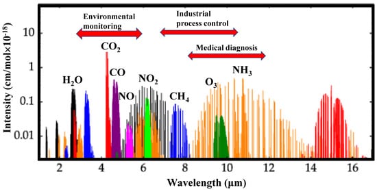
Figure 8. The relative intensities of specified compounds’ mid-infrared absorption spectra. H2O stands for water; CO2 stands for carbon dioxide; CO stands for carbon monoxide; NO stands for nitric oxide; NO2 stands for nitrogen dioxide; CH4 stands for methane; O3 stands for oxygen; NH3 stands for ammonia [152].
Long-wave infrared (6–14 μm) has great benefits for biochemical sensing since it covers a wide range of molecule absorption signatures [159]. WGs are an appealing chip-scale downsizing approach for optical sensors. Nevertheless, research on WG devices in this wavelength range is restricted. A suspended Si WG anchored by subwavelength grating (SWG) metamaterial claddings is used to construct a long-wave infrared photonic platform for quick and sensitive on-chip gas detection, as shown in Figure 9a–c [9]. This technology offers a practical method for fully using Si’s transparency window. The SWG structure offers a viable method for engineering the mode profile for strong light–analyte interaction. In the broad spectral region of 6.4 μm–6.8 μm, propagation loss and bending loss are explored. Grating couplers, for example, are useful devices. Y-junctions and directional couplers are also shown [9]. For instance, toluene vapor detection is used to demonstrate sensing that utilizes the technology. The detection limit corresponds to 75 ppm. Toluene at 75 ppm takes approximately 0.8 and 3.4 s to respond and recover, respectively [9]. The impressive results demonstrate that the system is a good fit for on-site medical and environmental applications.
On the MIR silicon-on-sapphire (SOS) framework, RRs have been realized [160,161,162]. Spott et al. published the first MIR SOS RR in 2010 [161]. The ring has a radius of 40 μm and a 0.25 μm edge-to-edge spacing. For λ = 5.4 to 5.6 μm, the experimental results revealed Q-factor = 3000, FSR at about 29.7 nm, and an associated group index of 3.99 [161]. A computational analysis of the design of a suspended membrane waveguide (SMW) made of SOI was performed in [159]. Using a 3D finite element approach, the WG architecture is tailored at 3.39 μm TE-polarized light, which is the absorption line of CH4 gas. The WG’s transmission loss (TL) and evanescent field ratio (EFR) are determined by various geometric factors such as core width, height, and cladding period. The relationship between TL and EFR has been discovered. As a result, WG architecture may be engineered to provide high EFR at the expense of high TL, or low EFR at the expense of low TL, as required [159].
For the monitoring of trace gases, optical WGs founded on the SOI platform provide an attractive substitute that uses EFA sensing. Gas sensors based on EFA can only operate if the gas in question has a specific absorption line at the operating wavelength. Furthermore, the optical attenuation at a certain wavelength is proportional to the gas concentration. The Beer–Lambert law, which is generally dependent on the gas concentration, length, and evanescent field ratio (EFR) of the WG, may be used to represent the power decay [163]. As a result, EFR is an important metric for detecting gas sensors based on EFA. The EFR is the ratio of the targeted region’s intensity integration to the WG structure’s overall intensity integration and can be written as:

Several gas sensors based on optical WGs [12,164,165,166,167] and optical fiber have been suggested to study this phenomenon. To manufacture gas sensors, there are multiple WG systems based on various platforms that may be used. Based on the concept of total internal reflection, the dielectric WG can direct light in a high refractive index core. At high WG cross-sections, these WGs enable significant mode confinement and typically minimal propagation loss. The evanescent field overlap in the ambient medium should be strong for highly sensitive EFA gas sensors. The propagating mode’s evanescent field can be increased by lowering the WG geometry at the expense of significant propagation loss. Furthermore, diffraction limits the capacity of these WGs to contain light.
Low evanescent field and high propagation loss may be solved with a hybrid plasmonic WG (HPWG) construction. A thin film of low index material (for instance SiO2) is layered between high refractive index material (such as Si) and metal in this WG (typically silver or gold). The horizontal and vertical variants of the HPWG are both possible. Air (n = 1.0) can be utilized as a low index material between metal and high index material in the horizontal layout. These WGs are extremely appealing for gas sensing applications because a hybrid mode is restricted in a low index nano-slot that may directly interact with the ambient medium. We established an EFR of 0.55 in prior work on strip, rib, and slot WGs [12,13,14,164]. For the monitoring of lethal CH4 gas, the EFR is improved in a more responsive dual-HPWG structure [165]. The WG shape is tuned for the absorption line of CH4 gas, which is λ = 3.392 μm. The modal parameters of a conventional ridge WG, such as EFR, E-field distribution, confinement factor, and propagation loss, are estimated. By placing gold rail on both sides of the core parted by a nano-gap, the ridge WG is changed into a dual-HPWG. With a propagation loss of 0.7 dB/μm, an enhanced EFR of 0.74 is achieved. Determining the degradation in transmission power due to absorption by the gas in the medium yields a S of 0.0715 (mW/concentration) for the proposed WG design [165].
For hydrocarbon emission control, a chip-scale MIR sensor was created in [168]. Amorphous Si optical strip WGs were used in the sensor, which was made using CMOS methods. Through λ = 2.70 μm to 3.50 μm, the WG showed a strong fundamental mode. CH4 and acetylene measurements were used to assess its sensing capabilities. The distinctive C–H absorption bands associated with CH4 and acetylene were discovered at λ = 3.29 μm–3.33 μm and λ = 3.00 μm–3.06 μm, respectively, established on spectral mode attenuation. At λ= 3.02 μm and 3.32 μm, real-time CH4 and acetylene concentration monitoring were also accomplished. As a result, the MIR WG sensor allowed for precise and fast hydrocarbon gas combination analysis. The width and height of the WG was 10 μm and 1 μm, respectively, with a well-cleaved end facet, which was crucial to limit the optical loss produced by scattering, as seen in the cross-sectional SEM picture in Figure 9d [168]. The butt-coupling efficiency between the 9 μm core diameter MIR fiber and the WG was enhanced by the 10 μm WG width. The asymmetric C–H stretching generated by C2H2 resulted in a significant absorption coefficient from λ = 3 μm to 3.08 μm. Due to the asymmetrical C–H vibration, the mode intensity for CH4 fell between λ = 3.18 μm and 3.40 μm. The significant R branch and the mild P branch of CH4 were ascribed to the absorptions detected at λ = 3.32 μm–3.40 μm and 3.18 μm–3.30 μm, respectively (Figure 9e) [168].
A polarization-independent HPWG tailored for λ = 3.392 μm, which corresponds to the CH4 gas absorption line is designed in [169] as shown in Figure 9f. Both TE and TM-hybrid modes can benefit from the WG design’s high mode S and EFR. The WG’s modal analysis is carried out using finite element methods in 2D and 3D models. The TE-hybrid mode can achieve mode S and EFR of 0.94 and 0.704, respectively, with adjusted WG variables, whilst the TM-hybrid mode can achieve mode S and EFR of 0.86 and 0.67, respectively. At 60 percent gas concentration, a 20-μm-long HPWG can dissipate 3 dB of power in the TE and TM hybrid modes as shown in Figure 9g and Figure 9h, respectively. The very sensitive WG system suggested in this work is thought to circumvent the polarization-controlled light’s limitations and might be used in gas sensing applications [169]. At 2.75 μm wavelength, μ-RRs on SOS were described [162]. The SEM image of the manufactured RR structure and ridge WG is shown in Figure 9i and Figure 9j, respectively. The resulting E-field mode profile, as illustrated in Figure 9k, was estimated using the finite element method. A Q-factor of 11,400 ± 800 was achieved. SOS wafer epitaxial Si thermo-optic coefficient was measured to be 2:11 ± 0.08 × 10⁴ K−1. Using a fixed wavelength source, a characterization approach for measuring the Q-factor of μ-RRs is also given. A MIR RR’s Q-factor may be measured simply by changing the device’s temperature. In situations when tunable lasers are not readily accessible, the suggested approach provides an alternate way of Q-factor measurement for μ-RRs in the MIR. At 2.75 μm wavelength, the approach was utilized to evaluate the Q-factor of SOS μ-RR [162].
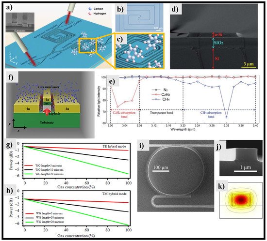
Figure 9. Si-MIR sensing devices, (a) suspended Si-WG gas sensing platform, which includes grating couplers, tapers, a power splitter (Y-junction), and spiral WGs, is depicted schematically. Inset: a cross-sectional view of the WG taken using an SEM [9], (b) optical picture of the Si spiral WG floating in mid-air [9], (c) a zoomed-in image of the sensing WG encircled by toluene molecules, as shown in Figure 8a by the yellow square box [9], (d) SEM photo of the Si WG [168], (e) when N2, C2H2, and CH4 were used, the WG mode intensities were measured. C2H2 showed strong intensity attenuation between λ = 3 μm and 3.08 μm, while CH4 showed strong intensity attenuation between λ = 3.29 μm and 3.33 μm [168], (f) HPWG enclosed in a gas sensor cell [169], (g) TE hybrid mode power variation vs. gas concentration [169], (h) TM hybrid mode power variation vs. gas concentration [169], (i) SEM picture of a racetrack RR [162], (j) WG cross-section as seen using an SEM [162], (k) FEM-calculated E-field mode profile of the matching quasi-TE mode [162].
This entry is adapted from the peer-reviewed paper 10.3390/photonics9050331
This entry is offline, you can click here to edit this entry!