Your browser does not fully support modern features. Please upgrade for a smoother experience.
Please note this is an old version of this entry, which may differ significantly from the current revision.
Industry 4.0 is a new paradigm of digitalization and automation that demands high data rates and real-time ultra-reliable agile communication. Industrial communication at sub-6 GHz industrial, scientific, and medical (ISM) bands has some serious impediments, such as interference, spectral congestion, and limited bandwidth. These limitations hinder the high throughput and reliability requirements of modern industrial applications and mission-critical scenarios.
- 5G
- 60 GHz
- Industry 4.0
- millimeter-wave communication
- smart antennas
1. Introduction
The fourth industrial revolution (Industry 4.0) is a paradigm of the cyber-physical world whose philosophy is based on fully automated and digitalized smart factories for enhanced production and customized user experience [1][2][3]. Various key enabling technologies are involved in one way or the other to bring the concept of Industry 4.0 to operation, such as cloud computing [4][5], big data [6], Industrial Internet of Things (IIoT) [4][5][7], digital twins [8], artificial intelligence [9][10][11][12][13], smart communication [14][15][16][17], additive manufacturing [18][19], advanced robotics [20][21][22], and cyber-physical systems [7][8]. The main objective of Industry 4.0 revolves around automation and mass-productivity without much human intervention. On the other hand, a more human-centric approach has been envisioned to propose a new generation of the industrial revolution, i.e., Industry 5.0 [23][24][25]. Its aim is to leverage human creativity in addition to the intelligence of machines [23][24]. However, it is instructive to mention here that since the philosophy of Industry 5.0 is based on human involvement back in an industrial environment, thus on technological grounds, most of the enabling technologies that serve to visualize Industry 4.0 can equally be employed to pursue Industry 5.0. Therefore, onwards in this entry, the researchers refer to both industrial regimes collectively as Industry 4.0 and beyond.
In the industrial regime, the communication network has already welcomed a shift from wired to wireless communication due to the unblemished benefits of wireless infrastructure, such as mobility, scalability, easy installation, and low cost [15][26][27]. Primarily, the industrial wireless communication infrastructure is based on sub-6 GHz industrial, scientific and medical (ISM) bands, such as 2.4 and 5 GHz [28][29][30][31][32][33]. However, under the ambit of Industry 4.0 and beyond, factory automation and smart manufacturing applications require high throughput, ultrahigh reliability with a packet error rate of up to 10–9, low latency of below millisecond level, and agility [34]. This requirement can be linked with one of the use cases of fifth-generation (5G) mobile technology, i.e., ultra-reliable low-latency communication (URLLC), as shown in Figure 1. Out of three vertices of a 5G triangle, i.e., enhanced mobile broadband (eMBB), massive machine-type communication (mMTC), and URLLC, the factory automation scenario fits best under URLLC category to ensure millisecond-level delay in smart communication [35][36]. Moreover, with the emergence of ever more sophisticated applications (such as holographic telepresence, virtual reality, augmented reality, visual capabilities for smart robots and automatic guided vehicles, mass customization and personalization of products), the sixth generation of wireless technology (6G) has also emerged as an enabling technology to enhance the efficiency and scalability of the communication system [37][38][39][40][41][42][43][44]. As a result, traditional sub-6 GHz wireless communication cannot meet URLLC requirements of Industry 4.0 and beyond because the unlicensed spectral resources in the low-frequency bands (e.g., 2.4 GHz and 5 GHz) are limited. The existing sub-6 GHz IEEE 802.11 wireless local area network (WLAN) standards (e.g., IEEE 802.11n, IEEE 802.11ac, etc.) can only provide a restricted data rate for new emergent applications.
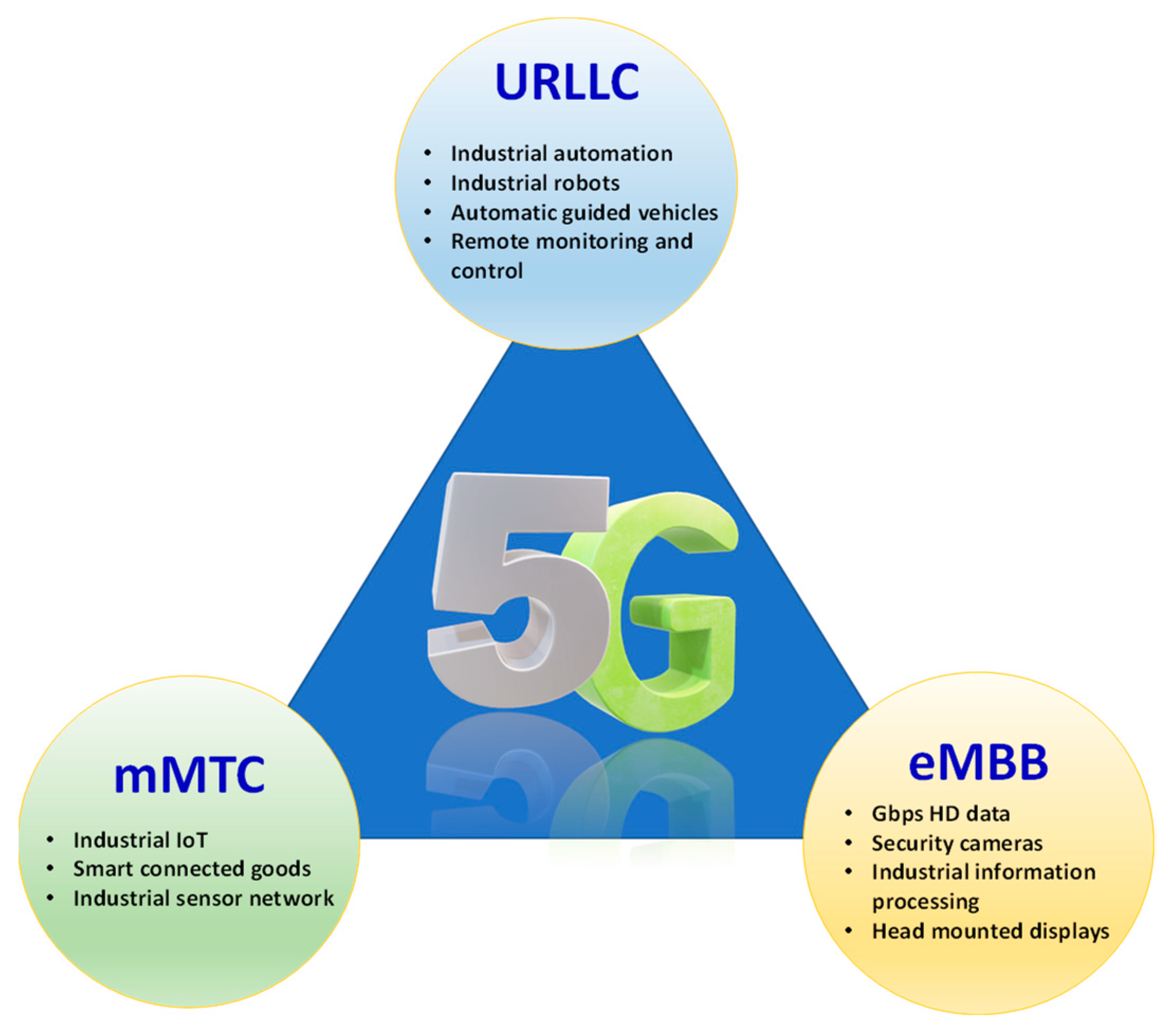
Figure 1. Avenues of 5G services in the viewpoint of Industry 4.0 and beyond.
In the context of Industry 4.0 and beyond, the requirements for quality of service (QoS) and quality of data (QoD) are much more stringent [28][41]. QoS mainly includes high reliability, real-time operation, agility, seamless connectivity, security, and privacy. QoD, on the other hand, includes validity, accuracy, and integrity of the data [28]. The 60 GHz mmWave communication carries a promising potential to provide high QoS and QoD. Some of the major key performance indicators in this view are illustrated in Figure 2.
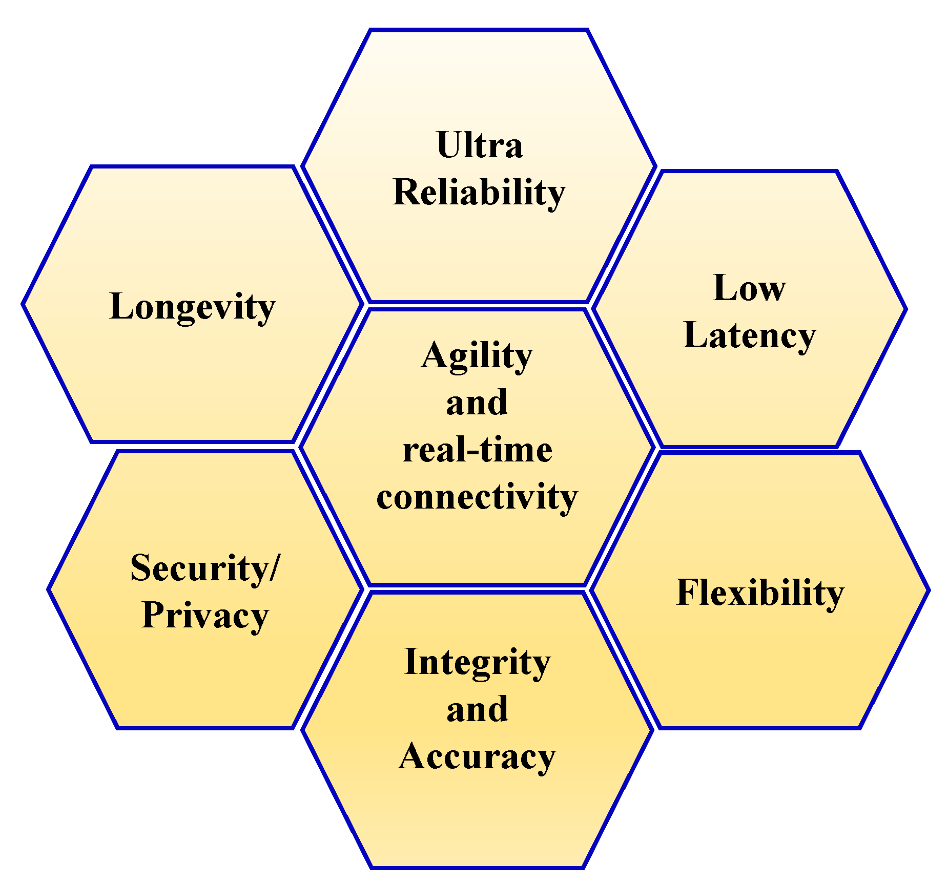
Figure 2. Key performance indicators for Industry 4.0 and beyond communication.
2. Antennas for mmWave Industry 4.0 and beyond Communication
Antenna design at the 60 GHz mmWave band has been explored to a great extent in recent years. This is due to the advancement in CMOS and IC design technologies that support compact mmWave circuitry and RF frontends. Array antenna systems with beamforming are essential to support robust and reliable communication due to smaller wavelengths at mmWave and high susceptibility to path loss. The beamforming antennas help to improve the coverage, SNR, and effective beam steering [45]. The researchers broadly categorize the 60 GHz smart beamforming antennas into three types: printed circuit board (PCB)-based antennas [45][46][47][48][49][50][51][52][53][54][55][56][57][58][59][60][61][62], on-chip antennas [63][64][65][66][67][68][69], and low temperature co-fired ceramic (LTCC)-based antennas [70][71][72][73][74][75][76][77][78][79][80][81]. The researchers discuss these antennas here in detail.
2.1. PCB-Based Antennas
PCB technology is cost-effective and easy to fabricate for antenna designs [82]. For mmWave antenna design, ease of fabrication and integration is of paramount importance. PCB technology is a common choice to fulfill these requirements. Moreover, the radiation properties of a particular antenna element are also an important consideration in the technology selection process. Broadside antennas are typically easier to integrate into array configurations, whereas end-fire radiating elements lend themselves best to edge integration. Microstrip patch antennas are currently among the most used radiating elements for 60 GHz mmWave arrays, despite material losses and performance limitations at this band. Various substrates are used to design such antennas, such as FR4, Rogers, liquid crystal polymers (LCP), polytetrafluoroethylene (PTFE), etc. [46][51][83][84][85]. For industrial communication, some other durable substrates are also reported in the literature, such as Arlon, but at lower frequency bands [86]. However, conductor and dielectric losses are quite high in PCB-based antennas at mmWave frequencies.
Because of the skin effect at 60 GHz, conductor losses increase manifold. A survey on various mmWave antenna designs from 10 to 100 GHz is presented in [82]. Many conventional PCB-based antennas such as microstrip patch, dipole, monopole and slot antennas are reported in the literature [46][50][51][57][60][62][87][88]. Moreover, Vivaldi antennas [89][90][91], dielectric resonator antennas [87][92][93], fractal antennas [94][95][96][97], and substrate-integrated waveguide (SIW)-based leaky wave antennas [61][94][98][99][100] are also implemented on PCB technology.
The key to enhancing antenna gain at the mmWave band is to use array configuration. A detailed overview of various mmWave array antennas, different array geometries, and the challenges in array configuration is presented in [82][101]. Microstrip-based array antennas at 60 GHz may suffer losses. The properties of the substrate and its thickness necessitate extra consideration. At 60 GHz, the substrate thickness is quite high when compared to sub-6 GHz microwave frequencies. This impacts the bandwidth and input impedance of the antenna. Moreover, proper feed structure is essential to be designed for accurate antenna performance [82]. Furthermore, a review of array antennas, including 60 GHz P2P and P2MP communication, is provided in [57].
2.2. LTCC-Based Antennas
LTCC technology has emerged in recent years for the miniaturization of portable electronics devices. It is a multilayer technology and eludes many disadvantages of PCB-based designs. LTCC is a multilayer technology that has been used for packaging ICs and has been applied to sensors, actuators, and integrated microsystems with relatively low cost and high productivity [72][75][102]. LTCC-based antennas can be employed with efficient characteristics in industrial environments as well. Various circularly polarized (CP) and linearly polarized (LP) LTCC-based antennas are reported [70][73][76][77][78]. Since the electric field of the wave only changes direction in a circular fashion in circularly polarized antennas, the signal strength remains constant. Thus, high gain CP antennas can be more useful for effective short-range communication in a rich scattering industrial environment. An LTCC-based phased array antenna at 60 GHz integrated with a 28 nm CMOS transceiver at 60 GHz was reported in [103].
In order to mitigate the high cost of large arrays at the 60 GHz band for beamforming or MIMO, a metamaterial-based LTCC compressed Luneburg lens antenna is reported at the 60 GHz band [79]. An assembly of stacked multilayer PCB was used to realize a high gain LTCC-based Luneburg lens antenna. A comprehensive review of various LTCC-based antenna designs at 60 GHz is presented in [72]. In the future, LTTC-based antenna designs can be employed in Industry 4.0 and beyond at 60 GHz as a low-cost and compact solution.
2.3. On-Chip Antennas
As a result of unprecedented development in integrated circuit (IC) design due to the unmatched level of integration and aggressive scaling of transistors in the last few decades, on-chip antennas have become part of the chip. Earlier, the system-in-package (SiP) approach was mainly used to include antenna design along with the chip. However, with this approach, the antennas, which have diameters on the order of wavelengths, are still outside the package and are still the bottleneck for true on-chip system realization [68]. More advancements and improvements in complementary metal oxide semiconductor (CMOS) and silicon germanium (SiGe) technologies have paved the way for the design of small-scale packaged antennas on silicon wafers using the system-on-chip (SoC) approach [63][68]. Moreover, for PCB-based antennas, the bond wires are used to connect antennas to ICs because they are typically implemented on PCBs. As a result, because these bond wires are not well characterized, matching can suffer greatly, especially at higher frequencies GHz band. In this way, on-chip antennas helped to alleviate this problem [68].
On-chip antenna configuration is governed by foundry-specific constraints, whereas on-chip antenna characterization necessitates the use of particular text fixtures. In recent years, the majority of on-chip antennas have been implemented in bulk silicon-based technologies such as CMOS and SiGe (with low resistivity of 10 ohm-cm), as opposed to other semiconductor technologies (with high resistivity) such as gallium arsenide (GaAa) [63][68].
Owing to smart manufacturing and integration techniques, these on-chip antennas can be integrated with moving objects, smart robots, moving machines, unreachable points in a factory scenario, and/or human head-mounts to provide indoor seamless connectivity at 60 GHz. Various on-chip antennas have been reported in the literature [63][67][68], among which monopole, dipole, loop, and Yagi-Uda antennas are fundamental types. An insightful demonstration of on-chip antennas, their design rules, characterization, limitations, challenges, and solutions are presented in [68]. The 60 GHz on-chip antennas, as well as the complete RF front end, are reviewed in [63].
3. Research Opportunities and Future Directions
Where there are challenges, there are opportunities. Millimeter-wave communication has opened many research opportunities in wide areas of communication systems. Some key opportunities and open research questions are discussed in this section.
3.1. RF Frontend Design
First, there exists a huge room for improvement and advancements to design efficient RF frontend components. For instance, mmWave power amplifiers are usually less efficient due to the very high frequency of operation. Similarly, the design of wideband PAs and low-noise amplifiers (LNAs) at 60 GHz mmWave is also a challenge [104]. Particularly high PA efficiency will help to extend communication range and enhance battery life. The phase shifters (e.g., to be used for phased array antennas) at mmWave frequencies are quite lossy, and thus, accurate phase shifts are difficult to achieve with low insertion loss. Lossy phase shifters also reduce antenna gain at high frequencies. Thus, research should be carried out to design efficient phase shifters at mmWave bands to reduce antenna losses. In the same way, other RF components, such as mixers and voltage-controlled oscillators, must have a very large tuning range at the 60 GHz band. Likewise, the design of high-speed digital to analog converters (DAC) and analog-to-digital converts (ADC) is also a challenge. ADC is a crucial component of the 60 GHz communication system as it determines the achievable data rates.
3.2. System-on-Chip Design
The advancement in CMOS, SiGe, and IC design has led to the design of on-chip antennas (AoC) and antennas-in-package (AiP). AoC has always remained a bottleneck for the realization of true system-on-chip (SoC) RF solutions. Efficiency is the main issue in AoC due to the low resistivity and high permittivity of a silicon substrate [68]. However, some solutions, such as CMOS-MEMS (microelectromechanical systems), to suspend the antenna structure in air and keep a gap from the silicon substrate, may increase the efficiency and gain of AoC [64][68]. Moreover, the characterization and measurements of AoC are also different than those of conventional PCB-based antennas. This is because on-chip antennas are fed using small wafer probes, which are fragile and prone to damage. Any mishandling may affect the measurement results. A microscope is required to accurately place the probes on the miniature on-chip antennas or the lines feeding the antenna. Microscopes are not standard anechoic chamber equipment, so they must be carefully placed so that they do not interfere with the antenna radiation or obstruct its movement [68].
3.3. mmWave Antenna Array Design Challenges
At mmWave frequencies, array antennas are crucial for high gain and directional communication. Array designs at mmWave frequencies face additional challenges compared to low-frequency arrays [105]. The antenna element is an important part of the phased array antenna design. It has to be chosen according to the requirements of the antenna array, such as operating bandwidth, gain, sidelobe levels (SLL), polarization, etc. [106]. Extra emphasis needs to be placed on array antenna gain (to compensate for high attenuation and path loss of mmWave), size, and interoperability with other radio frequency modules in mmWave communication systems [82][106]. The high directivity of mmWave beams should ensure that interference is minimized. The substrate materials used in mmWave array antennas also affect their performance. The thermal capacity of the substrate material also limits the power. Radiation pattern, bandwidth, input impedance, and efficiency are all influenced by conductor characteristics, substrate thickness, and relative permittivity values of the substrate [82][101].
Due to closely placed antenna elements in array configuration, the mutual coupling in proximity becomes an issue for antenna design engineers and needs special attention [82]. Mutual coupling between array elements causes grating lobes and power transfer from one element to another via direct radiation and surface waves. Careful selection of the gap between the antenna elements is necessary to avoid grating lobes [107]. In some cases, grating lobes are deliberately introduced to combat the sparsity of mmWave channels with an analog beamformer [108]. These intentionally created grating lobes are employed in an analog beamformer to increase the scattering intensity in NLOS settings and therefore increase the scattering in the received signal power delay profile. Mutual coupling at mmWave frequencies rises as the substrate becomes thicker, resulting in a greater number of surface wave modes. As a result, the array sidelobe levels and main beam shape are degraded and may also cause scan blindness [57]. Various methods to reduce the mutual coupling between array elements are reported in [109][110][111][112][113][114].
The polarization of the array antenna is also an important factor. Polarization is defined by the time-varying electric field vector at a given observation point. To overcome the polarization mismatch, multi-polarized antenna arrays are used with the improvement in diversity gain [115][116][117]. Polarization is also affected by mutual coupling. As the scan angle increases, the mutual coupling causes cross-polarization isolation to deteriorate [118]. To maintain polarization purity, polarization compensation techniques are sometimes used, which increase the cost and complexity of mmWave array design [119][120][121][122].
Appropriate feeding mechanisms and power division networks should be designed, and their effects should be included in the antenna design process. The performance of an array is degraded by the radiation from the feed network. Mitigating the feed connector losses in mmWave PCB-based antennas is a challenging task and demands special attention. Particularly, in an industrial environment, electromagnetic interference from other machines and electrical appliances may affect the antenna performance severely. In this way, complete electromagnetic modeling of the antenna system with respect to the industrial ambiance is necessary to achieve accurate performance of the antennas. Extra care should be given to the selection of antenna element type and material properties for industrial communication.
The development challenges in mmWave antenna beamforming networks are presented in [123] that need to be addressed in future research. The review of mmWave penetration, coverage, security, scalability, attenuation, and antenna array architecture is presented in [124][125]. In order to make a robust and efficient smart antenna system, the smart antenna systems should entail rigorous RF measurements in real industrial environments. This will help to fully characterize the propagation channels of industrial wireless systems over the mmWave band.
3.4. mmWave MIMO
Since 60 GHz IEEE 802.11ay standard supports MIMO configuration [126]; thus, more advanced MIMO techniques should be designed and experimentally analyzed for different antenna directivities and single-polarized or dual-polarized transmissions. Moreover, suitable research opportunities exist for the design and implementation of dynamic adaptive dual-polarized antenna arrays for millimeter-wave, as well as low-power and low-complexity MIMO systems [127][128] that allow for flexible analog and digital beamforming and advanced signal processing techniques. MIMO, massive MIMO, and multiple antenna techniques at mmWave bands are hot cake topics for researchers [129].
Furthermore, for the wideband properties of 60 GHz channels, severe hurdles for MIMO communications may be created, particularly in multi-user scenarios. A detailed survey of MIMO channel models in wireless communication is presented in [130]. It is worthwhile to investigate adaptable systems that adjust to changing channel circumstances to attain the required performance. Additional beamforming gain might be obtained by using a denser array. Directivity and spatial multiplexing gain are provided by a mmWave MIMO architecture with a series of sub-arrays [131]. As a result, the diversity in the spatial domain is fully used, enhancing communication resilience and resulting in exceptionally high SNR channel links that are practically fading-proof in an industrial environment. Furthermore, MIMO with beamforming has been reported to enhance PHY security at 60 GHz [132], which is an active area of research for Industry 4.0 and beyond.
3.5. Beamforming
Beamforming techniques created specifically for NLOS and LOS radio channels will be required for next-generation wireless communication systems. As the size of antenna elements is much reduced at mmWave bands and a large number of antenna elements are involved in an array configuration, thus mmWave beamforming requires more RF components and RF chains, which increases the complexity of the antenna system [133]. In this view, the huge room is available to perform research to devise efficient, less complex, and low-cost analog/digital hybrid architectures for smart antenna systems. In a factory environment, multiple antenna systems with numerous radiating elements at the access point are particularly interesting options for obtaining very high data rates (mGbps) for users sharing the same spectrum at the same time [123].
Furthermore, for an effective hardware implementation of a beamformer system operating in the mmWave band, a realistic understanding of hardware impairments, wave propagation, and antenna characteristics is required in industrial communication. Contemporary research challenges in mmWave beamforming include solving complicated challenges linked to analog/digital hybrid beamforming, polarization diversity, optimization of the beam search process, concurrent beamforming protocols, resilient adaptive beamforming, exploiting channel sparsity, and 3D beamforming. These systems must achieve the goals of lowering beamforming calculation costs, delays, and power consumption while maintaining acceptable QoS to provide mGbps throughput [134].
3.6. Terahertz Communication
Terahertz (THz) communication is considered an enabling technology to envisage beyond-5G and 6G systems [135][136][137]. Industry 4.0 and beyond can also benefit from THz communication for future mission-critical applications with the high demand for massive URLLC [138][139][140][141][142]. However, more difficult propagation conditions exist at THz frequencies, such as increased path loss, higher penetration loss, and more severe shadowing. Besides other challenges such as standardization, design of THz sources, THz integrated circuits, and advanced THz antenna fabrication techniques [143][144][145][146].
THz antennas are the key devices for THz communication because of their tiny size, wide frequency bandwidth, and high data rate [147][148]. A plethora of THz antenna designs are reported in the literature for THz communication [147][149][150][151][152][153][154][155][156][157], to list but a few. Graphene is extensively used in THz antennas due to its exceptional optical properties [151][158]. THz communication is believed to be an emerging and enabling technology in future Industry 4.0 and beyond to provide extremely high data rates, with open research challenges [138].
3.7. Distributed Antenna System
The relatively harsh environment in industries (as compared to homes, offices, etc.) demands robust communication solutions. Traditional co-located multi-antenna systems reduce path loss, but they are insufficient in demanding real-world industrial applications where NLOS conditions occur often [37][159][160]. URLLC in Industry 4.0 and beyond for cyber-physical systems is a crucial challenge that is anticipated to be served by distributed antenna systems at mmWave bands [161][162][163][164]. The potential of mmWave-over-fiber distributed antenna systems for high-data wireless communication was demonstrated in [161]. Measurements in a controlled anechoic chamber and a realistic environment resembling an Industry 4.0 setting revealed the potential of distributed antenna system for establishing and maintaining mGbps wireless communication while overcoming self-blocking and LOS blockage issues [161][165].
The link blockage problem must be carefully addressed in order to transmit mmWave signals through LOS pathways to the required users. This will result in effective coverage and smooth network connectivity for mmWave communication systems [106]. Distributed antenna systems can serve as a potential solution by adding the properties of mmWave communication systems [162][166].
3.8. Machine Learning for Antennas in Industry 4.0 and Beyond
The potential of exploiting machine learning (ML) is imminent in 5G and beyond-enabled Industry 4.0 and beyond. At each abstraction layer, ML is anticipated to be used to predict service demands of Industry 4.0 and beyond as well as the evolution of the wireless channel in order to design self-optimizing and self-updating networks [167][168][169][170]. It is unveiled in [161] that the traditional multi-antenna signal processing approaches are no longer sufficient for broadband mmWave massive MIMO systems due to a large number of radiating elements involved, high data rates, and a high number of mobile users. Unlike traditional communication systems, which demand many computing resources and result in unacceptable latency, deep-learning-based approaches take advantage of natural channel sparsity to efficiently precode and modulate data into several streams and send it to the distributed system [161][171][172][173]. Moreover, a physics-inspired neural network is used in [174] to design a reconfigurable coded metasurface for dynamic beam steering. Such type of ML-based reconfigurable antennas possess huge potential for Industry 4.0 and beyond applications, where the smart antennas system is required to reconfigure its radiation pattern in real-time based on blockage, jamming, and NLOS scenarios.
3.9. Reconfigurable Intelligent Surfaces
Reconfigurable intelligent surface (RIS) is a groundbreaking technique for reconfiguring the wireless propagation environment through software-controlled reflections to achieve enhanced spectral and energy efficiency in a cost-effective manner [175][176][177][178][179][180]. Some alternative terms are also used for RIS, such as intelligent reflecting surface (IRS) or software-controlled metasurfaces [181][182]. By changing the phase and/or amplitude, the elements of RIS can separately reflect the incident signal. In this way, beamforming for directional signal augmentation or null placement is performed. Radiating elements, control circuitry using PIN diodes or varactors, and a controller or field-programmable gate array (FPGA) [183][184]. RIS technology is still in its infancy; however, most of the development aspects of RIS are presented in detail in [185][186]. Furthermore, beamforming development with RIS is studied in [187][188][189].
RIS provides a unique and cost-effective method for proactively combating wireless channel impairments. In this view, RIS-aided industrial communication is an emerging research area with huge potential [178][190]. RIS-aided wireless communication carries the promising potential to be an enabling technology to assist smart communication in Industry 4.0 and Industry 5.0 [25]. Due to densely distributed industrial equipment (such as metal machinery, unpredictable movement of things (robots and trucks), wooden structures, and thick pillars), wireless signals are easily blocked and reduce performance reliability. When the direct communication link is impeded, RIS is a viable choice to provide an alternate transmission link [21][25][191][192]. The communication link can be created using a RIS mounted on the factory ceiling or the wall, delivering mission-critical industrial communication with seamless, reliable connectivity. A vision of RIS-enabled communication in Industry 4.0 and beyond seems to become a reality in the near future.
This entry is adapted from the peer-reviewed paper 10.3390/s22072688
This entry is offline, you can click here to edit this entry!