Many practical data-processing algorithms fail to execute efficiently on general-purpose CPUs (Central Processing Units) due to the sequential matter of their operations and memory bandwidth limitations. To achieve desired performance levels, reconfigurable (FPGA (Field-Programmable Gate Array)-based) hardware accelerators are frequently explored that permit the processing units’ architectures to be better adapted to the specific problem/algorithm requirements. In particular, network-based data-processing algorithms are very well suited to implementation in reconfigurable hardware because several data-independent operations can easily and naturally be executed in parallel over as many processing blocks as actually required and technically possible.
1. Introduction
Network-based data processing has attracted considerable attention due to recent advancements in reconfigurable computing, allowing complex and complete systems to be efficiently implemented and deployed in embedded applications. Field-Programmable Gate Arrays (FPGA) have been used to support parallel algorithm for decades, but it was a tight integration of reconfigurable logic with hard processing cores (both general purpose cores and graphics processing units) as well as latest advances in high-level synthesis tools that awoke more interest in network-based parallel data processing.
Network-based processing algorithms are characterized by a network of nodes, connected in a mesh so that data are processed by a number of nodes in parallel. Connecting processing units in a mesh/torus/fat tree is explored in many supercomputers, including IBM Summit
[1], Sunway TaihuLight
[2], and Fugaku
[3]. Supercomputing capabilities are definitely required in modern data centers but are not suitable for embedded systems due to constraints such as size, portability, power, and cost. The design of efficient embedded systems therefore involves different optimization criteria. Embedded systems have dedicated functions and can be optimized for particular operations in terms of execution time, existing real-time constraints, cost, and power consumption
[4].
FPGA have become more common as a core technology used to build electronic embedded systems. Moreover, Programmable Systems-on-Chip (PSoC) integrate reconfigurable logic with hardcore general-purpose and graphics-processing units, embedded memory blocks, high-performance interfaces, and specific-processing units (such as Digital Signal Processing (DSP) blocks) becoming complete, versatile, and programmable systems on a chip, steadily displacing general purpose processors and ASICs (Application-Specific Integrated Circuits). There are many reports of successful implementation of high-performance systems with FPGAs/PSoCs
[5][6][7][8][9][10][11][12][13][14][15][16][17][18][19][20][21][22].
2. Implementations of Parallel Networks in Reconfigurable Hardware
As it was illustrated in the previous section, various basic components (such as comparators or half-adders) belonging to the same network level can operate in parallel since they manipulate independent data. Therefore, such networks are very well suited to implementation in reconfigurable hardware, provided the number of components and levels can easily be customized to particular network parameters N and M. In this section, various implementation approaches will be analyzed and their advantages and pitfalls identified.
2.1. Implementations of Sorting Networks
Sorting is a very demanded operation in various fields, therefore a lot of research had directed toward optimizing executing this task. Sorting accelerators are often used in a very large number of systems beginning from simple embedded systems processing data received from sensors and ending with complex multichip-distributed computing systems that can be found in such areas as medical instrumentation, machine-tool control, communications, industrial networks, vehicles, agriculture, monitoring motorways, etc.
[23].
The first efficient implementations of sorting networks in FPGA have been reported 10–15 years ago, when the logic capacity of programmable devices has reached sufficient levels to compete with general-purpose and application-specific processing systems for solving computationally intensive problems. For example, Mueller et al.
[24][25] exploit the reconfigurability of FPGAs at runtime by reprogramming the chip for individual workloads, achieving high resource utilization and implementing data and task parallelism
[24]. Their implementations and experiments are targeted towards a Virtex-5 FPGA available on the Xilinx ML510 development board and running at 100 MHz. The authors analyzed bitonic and even-odd merge sorting networks and came to the conclusion that despite requiring more comparators, bitonic merge sorters are preferred because both the number of concurrent comparators for each level is constant (equal to N/2) and the delay for all signal paths is equal. For the selected bitonic merge network type, three alternative circuits have been studied: combinational (no clock), synchronous (exploring trade-off between the latency and clock frequency), and fully pipelined (allowing a new input data set to be applied every clock cycle). The authors did all the initial experiments, permitting to estimate approximately resources that would be required for instantiating a single M = 32-bit two-input comparator. That work permitted to conclude that the used Virtex-5 FX130T chip could accommodate just 1024 32-bit comparators. The implemented sorters were able to process up to N = 2
p=6 = 64 data items. The overall conclusion is that only small data subsets can be sorted in parallel in an FPGA-based accelerator therefore some software-based merger would make sense. When merging the sorted by the accelerator subsets in software, the speedup decreases with the increase of the data set size. The explanation is that the ratio between the work done by software (the CPU—Central Processing Unit) to work done in parallel in the accelerator decreases. Though no high speed-ups have been achieved over a CPU, the works
[24][25] provide the important step towards incorporating the capabilities of FPGAs into parallel data processing engines.
Zuluaga et al.
[26] affirm that sorting networks offer great performance but are prohibitively expensive for large data sets and propose tools to automatically generate a large set of candidate designs, which would lead to hardware implementations of sorting networks with reduced area, which are optimized for latency or throughput. A Domain-Specific Language (DSL) is introduced that permits different sorting networks to be represented. The designed DSL compiler generates Verilog Register-Transfer Level (RTL) descriptions for each desired design. To reduce the area cost, the suggested generator explores the regularity of the sorting networks to “fold” them by reusing sorting elements and constructing a variety of sequential datapaths. The resulting circuits are called “sorting networks with streaming reuse”. Experiments have been targeted to the Xilinx Virtex-6 XC6VLX760 FPGA using M = 16-bit input data. The authors report that the circuit with maximum reuse, which recurs to only one sorter, and the lowest throughput could be fit in the employed FPGA for N = 2
19, M = 16.
Sklyarov et al.
[27][28][29] performed analysis of different sorting networks and concluded that even–odd transition networks are among the most regular and easily scalable. As the
Table 1 confirms, even–odd transition networks are often characterized as considerably slower and more resource consuming comparing with even–odd merge and bitonic merge networks. However, the regularity of the even–odd transition networks permits simple iterative circuits to be designed with a main module composed of just two vertical comparator lines. Since the reused core module is identical for every pair of network’s levels, no multiplexers or complex interconnections are required, which would definitely be needed for bitonic merge and even–odd merge networks, leading to increasing propagation delays and decreasing throughput. A feedback N × M-bit register is inserted before a pair of vertical comparator lines and different levels are activated sequentially, still using many parallel comparison operations at each level. Initially N data items are copied in parallel to the register. Thus, there are N multiplexers at the register inputs taking data from outside (before processing) and from the second vertical line of comparators (during processing). Hardware resources are obviously decreased from N × (N − 1)/2 (see
Table 1) to N − 1 comparators. The resulting circuits are easily scalable to any N and the respective parameterizable VHDL specifications are given in
[23]. The overall throughput should be decreased as besides of executing the required by the network comparison operations, the register’s delay slows down the sorting. This is however not true because in practice the number of paths through the vertical levels of comparators is decreased when comparing to hardwired combinational sorting networks. This is because usually (not taking into account the worst case) the data become sorted at some stage earlier than passing through all the network’s levels (this situation is illustrated in
Figure 1 with the “sorted” label). The sequential sorter takes advantage of this fact and stops sorting as soon as at any stage no swaps in the vertical comparator lines are detected. Experiments realized on the Xilinx Zynq xc7z020 PSoC prove that no performance degradation is identified and the resources are reduced significantly, allowing constructing sorting circuits for N = 512/M = 32
[28]. The authors also called attention to the fact that although very interesting throughputs could be demonstrated by sorting networks themselves, such theoretical throughputs are not achievable in practice because of communication overheads. Indeed, initial data need to be supplied to the sorter (ideally, in parallel) and the results have to be taken from the sorter. So, trying to increase the number of sortable in parallel elements might be useless if there is no sufficient bandwidth to supply these elements to the sorter. To alleviate this problem, a communication-time sorter has been proposed in
[29] that is based on the network from
[27] permitting to find minimum and maximum values and enables data sorting to be completely overlapped in time with data transfers so that sorting is completed as soon as the last data item is received. Sorting subsets in an FPGA-based hardware accelerator and merging in software running on a hard processor in a Zynq PSoC has also been explored in
[29].
Najafi et al. propose a more area-efficient sorting network in
[30], which relies on unary processing. The idea is to encode every data item by a sequence of values ‘1’ followed by a sequence of values ‘0’ in a stream of 0’s and 1’s, such that the value is defined by the fraction of 1’s in the stream. Such an encoding permits to substitute conventional comparators by AND and OR gates. The authors report significant area reductions compared to traditional binary encoding but at the same time additional overhead is incurred by both conversion units which are required to encode the data from the binary to the stream format and a much longer operation time due to performing the operation on 2
M-bit long streams.
Norollah et al.
[31] suggest a multidimensional data sorter relying on matrix-based sorting suitable for real-time systems. The main achievements of the proposal are reducing the required resources and increasing memory efficiency, while experiencing a small negative impact on the execution time. Firstly, the authors propose organizing N input data in
matrix and activating
sorting networks to sort all the data. At each phase (out of six phases), each sorting network sorts its assigned either row or column items independently. Then, three-dimensional matrices are explored, leading to reduced resources but increasing the required number of sorting phases. Experiments executed on XC7VX485T FPGA of Virtex-7 family proved that the number of Look-Up Tables (LUTs) indeed dropped significantly when compared to a conventional bitonic merge sorting network, but the number of registers was increased (due to embedding a pipeline stage between each level in the network).
Srivastava et al.
[32] tried to solve the slow throughput problem in the merge sort and proposed a merge sort-based hybrid design where the final few levels in the merge sort network are replaced with “folded” bitonic merge networks. The authors tried to mix merge and bitonic sorting networks in attempt to alleviate their drawbacks. Thus, at the initial steps of the suggested sorting network merge sorting structure is employed, while the final steps recur to the bitonic method to increase parallelism. The experiments executed on the XC7VX690T FPGA confirm improving the throughput and reducing memory consumption.
Besides of the briefly characterized key works, other reports of efficient implementation of sorting networks in FPGA are recorded in the literature
[33][34][35][36].
2.2. Implementations of Searching Networks
Sklyarov et al. report the results of such implementation in
[23][27], considering two possible approaches: combinational and sequential. For the combinational implementation, the respective parameterizable VHDL specification is given in
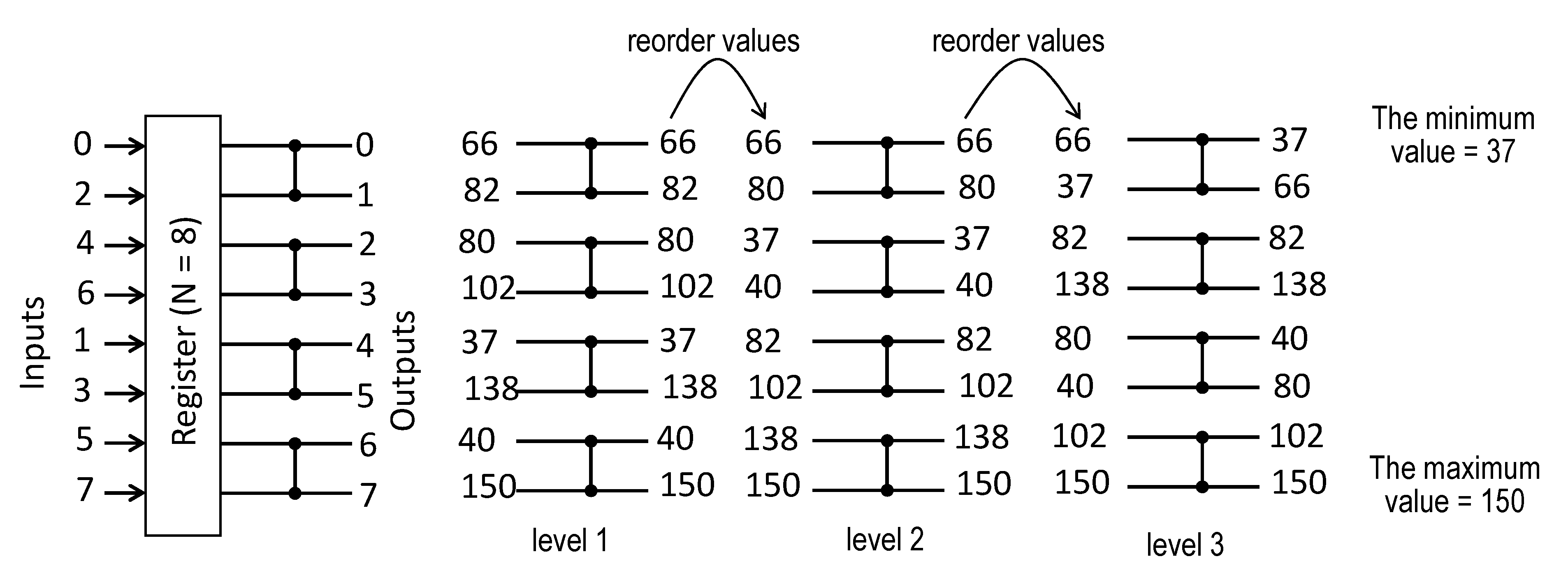
[23]. In the sequential circuit, illustrated in
Figure 1 for N = 8, a register is sequentially reused between the levels of comparators. The circuit is constructed such that even N/2 outputs 0, 2, 4, 6 of levels 1, 2 are connected with the upper N/2 inputs of the next levels 2, 3, respectively, and odd N/2 outputs 1, 3, 5, 7 of levels 1, 2 are connected with the lower N/2 inputs of the next levels 2, 3. Thus, outputs 0, 1, …, 7 depicted on the right-hand side of the register in
Figure 1 are fed back to the register’s inputs so that the lower input line is connected with the output 7, the line above the lower line is connected with the output 5, etc. Comparison of the networks in
Figure 1 suggests that any level executes a similar operation to the respective iteration in
Figure 1. Outputs after the first iteration in
Figure 1 are the same as the outputs of the first level. Subsequent iterations give similar results as the respective level, but the values are reordered as described above. Such sequential implementation permits the required hardware resources to be reduced. While the network uses C(N) =
comparators, the circuit in
Figure 1 functions with just
comparators. The implementation in
Figure 1 is regular, easily scalable for any N, and does not involve complex multiplexing schemes. The minimum and maximum values are found in L(N) =
clock cycles. The results of experiments reported in
[23] show that the throughput of the networks in
Figure 1 is almost the same.
Figure 1. Network of comparators with a feedback register for finding the minimum and the maximum data items.
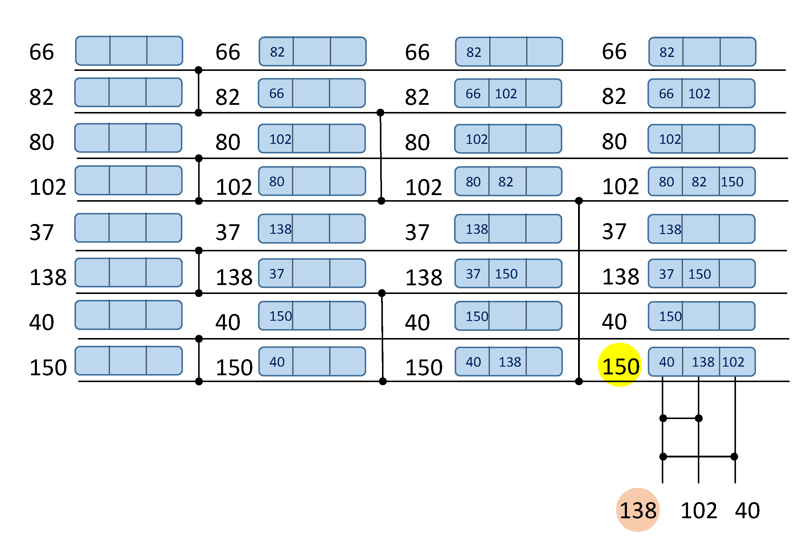
When two maximum/minimum values have to be identified, the networks can be implemented as is. Wey et al.
[37] suggest that the number of comparators could be reduced if keeping track of the compared data items at each level. The respective algorithm for N = 8 is illustrated in
Figure 2. Here, each data element requires a small memory, keeping at most L(N) data items. After every comparison operation, these memories need to be updated for the involved data items. For example, in the first level of comparators (the left-hand side of
Figure 2), the first comparator analyzes the data items 66 and 82. Consequently, the value 82 is written to item 66 memory and the value 66 is written to item 82 memory. After executing all L(N) comparator levels the largest data item (150) can be read from the bottom horizontal line, as before. However, to find the second largest value (138) just L(N) − 1 = 2 additional comparators are required that would only analyze data values recorded in the memory of 150 (i.e., data values 40, 138, and 102 in the example of
Figure 2). As the result, the required number of comparators is reduced to: C(N) = N + L(N) − 2. For big values of N the resources (number of comparators) are diminished considerably, but additional memory requirements as well as memory management introduce an overhead. The authors also explore a tree structure search approach in
[37] and conclude that while this approach achieves higher speed performance, it requires a greater number of comparisons.
Figure 2. Network of comparators with memory for finding two largest data items: 150 (highlighted with yellow color) and 138 (highlighted with orange color).
The bit-searching approach proposed by Tzimpragos et al. in
[38] allows several minimum or maximum values to be found. Here, the search is not based on comparisons between the elements of a dataset. Instead of this, the items’ bits are scanned from MSB (Most Significant Bit) to LSB (Least Significant Bit) with the aid of filters constructed from FPGA LUTs. This scheme works very well for small data items (whose number of bits M ≤ 3–4) but is not efficiently scalable for greater values of M. The authors report that for M > 4, the previous, described above approaches are less resource-consuming. A positive aspect of this solution is that the number of needed stages does not increase with the input size N.
2.3. Implementations of Counting Networks
Counting networks can be used efficiently for calculating the Hamming weight (HW) of binary vectors. This operation has many practical applications, such as binarized neural networks, cryptography, telecommunications, cheminformatics, bioinformatics and others
[39]. Besides simply counting the HW, certain applications require the HW to be compared to either a fixed threshold or to the HW of another binary vector (possibly of a different length). The respective network-based implementations will be briefly characterized below.
Pedroni proposes a network-based Hamming weight comparator circuit in
[40] relying on a triangular bit sorter circuit composed of M × (M − 1)/2 nodes with two gates (AND and OR) per node. The bit sorter sorts all the bits on the input binary vector. Then, if an output j, j = 1, 2, …, M is equal to 1, it indicates that the input vector has HW equal to or greater than j. The author gives a complete parametrizable VHDL code, allowing the design to be tested on an FPGA and also reports the results of implementation on the EPF10K20C240 FPGA.
Piestrak has improved on the previous results using sorting networks of lower time and cost complexities and suggested combinational digital comparators built using multioutput threshold circuits
[41]. The complexity and latency estimation is executed but no hardware implementation details are provided.
Parhami also addresses the problem of Hamming weight comparators and proposes efficient circuits based on accumulative and up/down parallel counters in
[42]. First, the author suggests using a network of parallel counters, adding the sum of M increment signals to a stored count (which has
bits). The HW count part of the design consists of a tree of increasingly wider ripple-carry adders. A fixed-threshold HW comparator is obtained if the arithmetic negation of the threshold k, that is, −k, is placed in the count register at start. Then it is only necessary to check whether the final count result is positive or negative. In the up-down parallel counters, the inputs are interpreted as signed count signals (increments and decrements), each encoded in 2 bits. These permit the comparison of the HWs of two vectors of the same length (one vector ‘1’ bits are considered to be positive values +1 and another vector ‘1’ bits are considered to be negative values −1). The author also presented a detailed cost and latency theoretical analysis of the previous three designs, concluding that his proposal exhibits better characteristics. No hardware implementation results are however reported.
Sklyarov et al.
[23][43] suggest hardware circuits based on counting networks. Several types of counting networks are analyzed and compared, such as pure combinational, partially sequential with reusable fragments, and pipelined. HW comparators are also proposed one of which is based on carry-network blocks from
[42] and the other one recurs to LUTs. A single LUT(n,1), i.e., a LUT with n inputs and 1 output, can be configured to support any threshold k < 2
n. It is also suggested how to deal with k >> 2
n. The proposed designs are not based on sorting networks, leading to more modest hardware resources. This is because, in contrast to sorting networks, the number of the used basic components in counting networks is incrementally reduced as data move from left to right. Thus, albeit the number of levels is the same (when compared to the number of levels in the best sorting networks), due to incrementally reduced complexity at each level, counting networks can be employed for a significantly greater value of M than sorting networks (within the same target hardware constraints). The authors report the results of experiments on two FPGA/PSoC-based prototyping boards: the Atlys with the Xilinx Spartan-6 FPGA and ZedBoard with the Xilinx Zynq including Artix-7 FPGA that prove that the proposed counting networks outperform the previous parallel counter-based designs. It is also illustrated that counting networks can be mapped efficiently to DSP slices that are available as standard components in modern FPGAs.
LUT-based circuits are explored in
[44] where firstly, two optimized LUT-based designs that permit the Hamming weight to be determined for M = 8 and M = 36 are suggested. The Hamming weight for M > 36 can be calculated in a tree-based structure. A combination of counting networks, LUT- and DSP- based circuits is proposed in
[45]. It is noticed that LUT-based circuits and counting networks are the fastest solutions for small values of M (M ≤ 128 bits). The result for bigger vectors (M >> 128) is produced as a combinational sum (executed in either DPS slices or in a circuit built from logical slices
[45]) of the HWs of the sub-vectors.
This entry is adapted from the peer-reviewed paper 10.3390/electronics11071029