Your browser does not fully support modern features. Please upgrade for a smoother experience.
Please note this is an old version of this entry, which may differ significantly from the current revision.
Subjects:
Engineering, Electrical & Electronic
With the increase in the demand for high-speed transmission communication, satellite communication is developing rapidly. Because of the bandwidth capacity, the K/Ka band is considered the mainstream frequency band of satellite communication. The performance of a power amplifier (PA) directly affects the power of the transmitter, so the application of a power amplifier in Ka-band satellite communication is very important.
- power amplifier
- Ka band
- satellite communication
1. Introduction
Satellite communication has the characteristics of wide coverage, large capacity, and long communication distance, and is not limited by the geographical environment. It is widely applied in broadband multimedia communications, personal mobile communications, military communication, and other fields. In the long-term development process, satellite communication and mobile communication form complementary relationships, playing an irreplaceable role [1].
At present, the frequency bands used in satellite communication mainly include the L band, S band, C band, Ku band, and Ka band. In the past decade, with the continuous development of the satellite application field, spectrum congestion has occurred in the conventional frequency bands L band, S band, and C band allocated by satellite services [2]. Limited by bandwidth, the communication rate of these satellites is becoming more and more difficult to meet the needs of information society for high-speed data transmission. In this case, Ka-band broadband communication satellite technology has entered the field of vision of various countries and become the research goal of various countries because of the wide available frequency band (26.5 GHz~40 GHz) and few interference signals.
In 1997, the U.S. Federal Communications Commission (FCC) issued Ka-band satellite communication licenses to more than a dozen companies to promote the development of Ka-band satellite communication technology. These high-tech companies include Motorola’s Celestri system, Lockheed Martin’s Astrolink system, GE Americom’s Ge star system, and others [3]. After years of development, the Ka-band broadband multimedia communication satellite in the United States has been put into commercial use, which can provide high-speed broadband Internet access services for rural families in remote areas and airliners.
Because the rain attenuation of the Ka band is greater than that of the Ku band, the requirements for devices and processes are higher, and satellite communication in the Ka band developed slowly in the past [4]. With the improvement in the hardware manufacturing level, Ka-band microwave circuits have developed rapidly over the past 10 years.
In October 2011, the full Ka-band communication satellite ViaSat-1 of VIASAT was successfully launched [5]. The total communication capacity of ViaSat-1 exceeds 140 Gbps, which is more than 70 times that of any Ku-band satellite at that time [6]. In particular, with the launch of the new generation satellite ViaSat-1, the concept of the high price and narrow bandwidth of traditional satellites has been changed. The transmission speed provided by the satellite is higher than that of terrestrial digital subscriber line DSL and wired cable, but the service price of users is almost the same [7]. In 2012, ViaSat-1 was officially put into commercial use, opening a new era of Ka-band satellite communication [8].
In addition to the field of satellite communication, the next generation mobile communication technology 5G is also likely to use the communication technology of the Ka band. Regarding 5G, the Third-Generation Partnership Project (3GPP) determined the millimeter-wave band 26 GHz/28 GHz/39 GHz as the 5G band to be deployed first in the world [9].
In recent years, many high-tech companies in the United States and South Korea have successively completed the verification test of the 5G communication prototype based on a 28 GHz band [10]. Whether for 5G or broadband communication satellites in the future, Ka-band applications can provide high-speed communication services. With the maturity and promotion of these technologies, there will be a lot of demand for Ka-band communication systems in the future.
As an important part of the transmitter in the communication system, the performance of the power amplifier plays a decisive role in the performance of the whole system. Figure 1 is a block diagram of a communication system transmitter. Usually, the power amplifier is located at the end of the transmitter of the whole communication system. After the signal passes through the modulator, mixer, and band-pass filter, it is amplified to a certain power level through the power amplifier and transmitted through the antenna. Among these modules of the communication system, the power amplifier is a core module. Its linearity directly determines the transmission signal quality of the transmitter, its efficiency determines the power consumption of the transceiver, and its output power determines the distance of communication. Therefore, designing a power amplifier with good performance is the key to determine the quality of wireless communication. Therefore, the research of the power amplifier is very important.

Figure 1. A block diagram of a communication system transmitter.
2. Technology
There are several semiconductor processes that have been demonstrated for power amplifiers at the Ka band. They are gallium arsenide pseudomorphic high electron mobility transistors (GaAs pHEMT) [11], gallium nitride high electron mobility transistors (GaN HEMT) [12], indium phosphide heterojunction bipolar transistor (InP HBT) [13], silicon complementary metal–oxide–semiconductor (Si CMOS) [14], silicon and germanium bipolar complementary metal–oxide–semiconductor (SiGe BiCMOS) [15] and silicon on insulator complementary metal–oxide–semiconductor (SOI CMOS) [16].
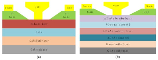
In the late 1970s and early 1980s, the HEMT structure was proposed and developed [17,18]. During this period, a number of research groups around the world proposed the AlGaAs/GaAs crystal structure, collectively known as HEMT. The traditional GaAs HEMT structure profile is shown in Figure 2a [19].

Figure 2. (a)Traditional GaAs HEMT structure profile, (b) GaAs pHEMT structure.
However, there exists a deep donor state trap DX center in the AlGaAs/GaAs heterojunction, which causes device degradation at low temperatures [20]. To solve this problem, Phemt was invented.
In 1986, A. Ketterson first fabricated the AlGaAs/InGaAs/GaAs Phemt structure on a GaAs substrate [21]. The GaAs Phemt structure is shown in Figure 2b.
GaAs Phemt solves the above problems by introducing the AlGaAs isolation layer, which is used to isolate the two-dimensional electron gas (2DEG) layer and doping layer [22]. Compared to HEMT devices, Phemt greatly improves electronic transport characteristics. The electron mobility velocity of GaAs is 5 or 6 times that of Si and has higher drift velocity and better high frequency characteristics [23]. In recent years, Phemt’s cut-off frequency fT
and maximum frequency fMAX reached 360 GHz and 400 GHz, and they are widely used in millimeter-wave frequencies [24]. However, GaAs has high thermal resistance and low breakdown voltage, which limits its application in high voltage and high power. In 2018, Aviv Barabi presented a PA targeting more than 25 Db gain and 27.3 dBm output power between 96 and 98 GHz adopting 0.1 μm GaAs Phemt [25]. In 2020, Ref. [26] proposed a 3-stage CS PA in 65 nm CMOS, achieving 13.4 dBm saturated output power (Psat
) with peak PAE of 11.3% in the 85–101 GHz range. Compared with CMOS process, the GaAs process has the advantage of high output power at higher frequency.
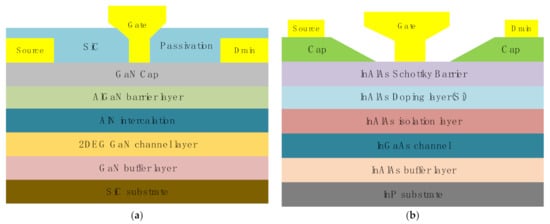
GaN HEMT and GaAs Phemt devices operate on a similar principle and are both high electron mobility transistors operating through 2DEG [27]. However, due to GaN’s special spontaneous polarization, GaN HEMT can also produce 2DEG without doping. The profile of GaN HEMT is shown in Figure 3a.

Figure 3. (a) GaN HEMT structure profile, (b) InP HEMT structure profile.
GaN and GaAs have similar frequency characteristics, but due to the special spontaneous polarization of GaN, the concentration of 2DEG is one order of magnitude higher than that of GaAs [28]. Therefore, GaN has high current density and outputs high power at high frequency. In 2018, M. Roberg presented a GaN MMIC Pas using Qorvo’s QgaN15 released process. The output power of the reported PA is approximately 46.2 dBm at 27.5–29.5 GHz [29]. The substrate selection of GaN is a key problem. GaN devices grown on a SiC substrate can obtain higher performance, but the cost is very high. Therefore, several research groups regard GaN on the Si substrate as a feasible solution for the large-scale market application, and massive commercial products have been designed and manufactured. However, compared with the SiC substrate, the Si substrate has worse electrical and thermal properties [30]. The cost and performance must be considered comprehensively to select a more appropriate scheme. In a word, the GaN process can bring some advantages of III-V technology (III-V compound semiconductor technologies include GaAs, GaN, InP, etc.) and its price is lower than the GaAs technology due to the possibility of integration on the Si substrate.
In the research of high frequency electronic devices, the transistors using InP materials are adopted in HEMT and HBT technology. The InP HEMT device is a vertical device, which has better noise characteristics than the InP HBT device. It is often used to design low-noise amplifiers. Its profile is shown in Figure 3b.The InP HBT device is a transverse device. Compared with InP HEMT, its breakdown voltage is higher, and its power capacity is larger. It is often used to design power amplifiers.
InP HBT is mainly divided into a single heterojunction bipolar transistor (SHBT) and a double heterojunction bipolar transistor (DHBT). On the one hand, the band gap of the InP DHBT collector material is greater than that of the InP SHBT collector material, so its collector has higher voltage resistance, and it is conducive to high power output; on the other hand, the collector material of InP DHBT has high thermal conductivity, so it has better heat dissipation performance and is more suitable for high-current and high-power circuit design.
InP-based technology is the only technology that can provide Pas with >20 dbm output power over 200 GHz [31,32]. DHBT 500 nm and 250 nm technology nodes provide about 330 GHz and 400 GHz fT
respectively, and the latter’s fMAX
is up to 700 Ghz. Compared with traditional CMOS FET, the InP DHBT process has the advantages of large breakdown voltage, small parasitic capacitance and low substrate loss. The main limitation of InP is its cost because it is difficult to purchase and is a very fragile material, which makes its manufacturing and handling extremely dangerous.
With the increase in the operating frequency of Pas, the CMOS process node decreases to several nanometers or tens of nanometers [33]. The reduction in the MOS transistor size will reduce the breakdown voltage threshold of the gate oxide layer, and the power supply voltage will also decrease with the increase in the process nodes. Silicon has low electron mobility and poor high frequency characteristics, which limits the application of silicon technology in the higher frequency band. The lower breakdown voltage also limits the output power of the power amplifier.
However, due to the extremely rich content of silicon in nature, it is easy to purify and grow a single product. The cost of silicon technology is much lower than that of III-V technologies (when mass produced). In addition, the integration of silicon technology is very high, and multi-layer metal layers can make very complex circuits. In 2021, J. Park proposed a 2-stage cascode PA in 60 nm CMOS. The PA achieved 17.1 dBm output power and the PAE remained above 38.2% in the area of 0.16 mm2 [34]. When the performance requirements are not too strict, the silicon process can be realized in a small area, and the cost is very low. Therefore, silicon technology is one of the important processes for making the Ka-band power amplifier.
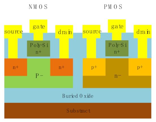
With decades of development, bulk silicon CMOS technology has become more and more mature. However, with the continuous reduction in device feature size, many new problems still appear, such as the short channel effect. SOI (silicon on insulator) technology refers to the process of forming a layer of semiconductor monocrystalline silicon thin film material on the insulating material layer, and then manufacturing integrated circuits on monocrystalline silicon. The main difference between the traditional bulk CMOS process and SOI technology is that SOI CMOS have a buried oxide layer, which separates the device from the substrate [35]. Its profile is shown in Figure 4. In SOI CMOS, each device is surrounded by an oxide layer, which is completely isolated from the surrounding devices and fundamentally eliminates the latch-up effect [36]. At the same time, the buried oxygen layer also increases the thickness of the insulating layer between the interconnect and the substrate, which greatly reduces the parasitic capacitance of the interconnect [37]. Reducing the capacitance is helpful to improve the speed of the circuit and reduce the power consumption of the circuit. IBM 45 nm CMOS SOI technology has been widely used in the development of millimeter-wave power amplifiers [38,39,40]. It provides SOI CMOS transistors with very high fT
and fMAX
(>400 GHz) [41]. The excellent performance of SOI MOSFET makes the SOI CMOS circuit more suitable for working in harsh environments, such as aerospace and high temperature.

Figure 4. SOI CMOS structure profile.
However, SOI CMOS process technology cannot replace bulk silicon CMOS technology, mainly because the SOI CMOS process is not as mature as the bulk silicon CMOS process. The quality of the silicon film of SOI material is not as good as that of bulk silicon material. In addition, the cost of SOI CMOS is higher than that of bulk silicon CMOS.
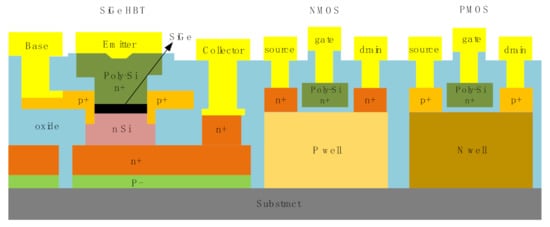
The development of SiGe devices is mainly promoted by IBM and other companies. The BiCMOS process is adopted, which can be used as an alternative to CMOS. BiCMOS technology is a new technology that integrates bipolar transistor (BJT) and field-effect transistors (FET) on the same chip. Compared with CMOS, under the same scale, the performance and cut-off frequency of the SiGe device are greatly improved, and it is better than the silicon-based CMOS device in withstanding voltage and the current processing ability, so it is also suitable for medium power applications. As shown in Figure 5, SiGe BiCMOS combines SiGe HBT applied to the RF circuit and SiGe CMOS applied to digital circuit, combining the digital and analog on one chip. Compared with traditional Si BiCMOS, SiGe BiCMOS is more conducive to integration. In the past 10 years, SiGe BiCMOS technology has been greatly developed, breaking through the technical barriers of 0.35, 0.18 and 0.13 um. The cut-off frequency fT
of SiGe HBT has reached 40~350 GHz, and the maximum operating frequency can almost reach the level of GaAs [42]. It has strong competitiveness and wide application prospects in the RF field.

Figure 5. SiGe BiCMOS structure profile.
In the author’s opinion, GaN and GaAs materials have power advantages for chips with an operating frequency not higher than 100 GHz. If frequency is the primary consideration of the device, the frequency of the power amplifier made of the InP device can be higher than 500 GHz. Of course, for industrial manufacturing, the product cost is also an important factor in the power amplifier design and mass production. Especially for consumer electronics, CMOS is conducive to system-on-chip integration, so it has a cost advantage. In addition, the loss of performance or quality factors of passive components are quite competitive [43].
This entry is adapted from the peer-reviewed paper 10.3390/electronics11060942
This entry is offline, you can click here to edit this entry!
