In the development of hydrogen-based technology, a key challenge is the sustainable production of hydrogen in terms of energy consumption and environmental aspects. However, existing methods mainly rely on fossil fuels due to their cost efficiency, and as such, it is difficult to be completely independent of carbon-based technology. Electrochemical hydrogen production is essential, since it has shown the successful generation of hydrogen gas of high purity. Similarly, the photoelectrochemical (PEC) method is also appealing, as this method exhibits highly active and stable water splitting with the help of solar energy. We discuss the exceptional optical and electrical characteristics of perovskite materials which often dictate PEC performance. We further extend our discussion to the material limit of perovskite under a hydrogen production environment, i.e., that PEC reactions often degrade the contact between the electrode and the electrolyte.
- Metal-organic halide perovskite
- photoelectrochemical reaction
- water splitting
Intrinsic Properties of Perovskite Materials
The general molecular formula of perovskite is ABO3; perovskite materials have a cubic lattice-nested octahedral layered structure. These materials have superior magnetic, ferroelectric, electrical, and optical properties, attracting attention for potential use in optoelectronic devices. At present, many research groups are actively investigating these characteristic properties, and recently, nuclear magnetic resonance (NMR) spectroscopy has been significantly used for analyzing the structure of these perovskite materials [1]. Perovskite materials also have low recombination probability and high carrier lifetimes and diffusion lengths [2][3]. Therefore, metal-organic halide perovskites have been amongst the most interesting subjects in optoelectronic materials research, and are utilized in various fields such as light-emitting diodes, solar cells, lasers, and photodetectors [4][5][6][7].
1.1 crystal structure
The metal-organic halide perovskite has a molecular structure of type ABX3, where A and B are cations (A is larger than B), and X is the anion. The general crystal structure of perovskite is shown in Figure 1a–c [8][9]. Perovskites commonly have unit cells consisting of five atoms in a cubic structure (α phase), where the A cation (methylammonium, CH3NH3+, MA+, or formamidinium, CH(NH2)2+, FA+) is surrounded by twelve X anions (Cl−, Br−, or I−, or a coexistence of several halogens) to form a cuboctahedron, and the B cation (Pb2+, Sn2+, etc.) is located at the octahedral site of X. The B cation–X anion octahedra are joined together to form stable three-dimensional network structures [3][10]. To achieve a cubic structure with a high degree of high symmetry, i.e., an ideal perovskite crystal structure, the radius ratio of A, B, and X should be such that tolerance factor {t = (RA + RB)/ RB + RX)} is close to 1 [11]. For the tolerance factor to approach 1, the A cation must be much larger than the B cation. In metal-organic halide perovskite, the A site must be occupied by a very large atom because the B site is usually occupied with a large atom such as Pb or Sn. Tolerance factors of cubic structures are generally between 0.89 and 1, where a tolerance factor lower than 0.89 could induce a tetragonal (β phase) or orthorhombic (γ phase) structure, whereas higher tolerance factors could induce a two-dimensional (2D) layer structure due to the unstable three-dimensional (3D) B–X bonding [12][13][14]. Actually, the transverse phonon easily displaces the X anion from the B–B intermediate location of the cubic structure [15][16]. The non-perovskite δ phase appears in perovskite materials such as HC(NH2)2PbI3, FAPbI3, CsPbI3, and CsSnI3, which, unlike the β and γ phases, is caused not by B–X–B angle distortion in the α phase, but by the breaking of the B–X bond [17][18][19].

Figure 1. Crystal structure of perovskite materials. (a) A typical perovskite crystal structure. (b) Crystal structure of B cation and X anion (B cation is located at the octahedral site of X anion). (c) Crystal structure of A cation and X anion (A cation is located at the octahedron site of X anion.
1.2 Optical properties
As one of the unique properties of metal-organic halide perovskites, the optical properties of photo-generated charge carriers have been researched. The specific excitonic absorption peaks of the metal-organic halide perovskite could be transited to various absorption spectra, and it changed significantly in visible light through the adjustment of metal atoms and halogens (Figure 2a, b). Converting the metal atom directly changes the M–X bonding, resulting in changes in valence band maximum and conduction band minimum, as the band edge is determined by the metal orbitals of the B site. In fact, in perovskite, the valence band is composed of 5p orbitals of I and the s-antibonding states of Pb 6s. The conduction band is composed of 5s orbital of I and the s-antibonding states of Pb 6p. For example, when the B site is changed from Pb to Sn in MAPbI3, the bandgap changes from 1.57 to 1.17 eV, and therefore, the bandgap between 1.57 eV and 1.17 eV can be controlled by adjusting the ratio of Pb and Sn [20][21]. Additionally, converting the A organic cations changes the length and angle of the M–X–M bonding, which, in turn, changes the bandgap but does not affect the valence band maximum. In fact, MAPbI3 shows a rapid absorption rise at 825 nm (1.5 eV) and has a large absorption coefficient of 1.8 × 104 cm−1. By substituting the methylammonium (MA) cation with formamidinium (FA), the energy bandgap could be lowered to 1.48 eV, which reduces the bandgap by 0.09 eV and allows for additional light absorption [22]. Metal-organic halide perovskites are widely used in the optoelectronics field due to their excellent and wide-ranging absorbance in the visible light range [23]. Furthermore, metal-organic halide perovskites could exhibit amplified spontaneous emission due to the low defect density and slow Auger recombination, even in the presence of electron and hole extinctions [24][25]. The absorption coefficient of perovskite is affected by temperature, tending to decrease at lower temperatures. This is associated with the interaction of excitons and phonons at low temperatures and the phase transition of MAPbI3 at about 160 K (Figure 2c) [26]. Similar to light absorption, the photoluminescence (PL) of metal-organic halide perovskite could be tuned by changing organic cations or anions. In the case of MAPbI3 quantum dot (QD), the PL spectrum could be tuned from 407 to 734 nm by changing the composition of anions (Figure 2d) [27]. Due to its properties to tune the strong PL spectrum, perovskite is utilized in a variety of light-emitting applications including lasers, light-emitting diodes, and optical sensors [21][28][29][30].
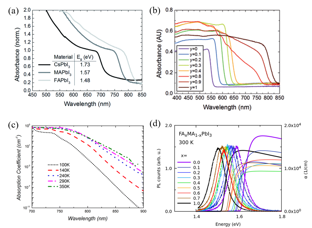
Figure 2. Optical properties of perovskite materials. (a) UV-vis spectra for the APbI3 perovskites formed, where A is either cesium (Cs), methylammonium (MA) or formamidinium (FA). (b) UV-vis absorption spectra FAPbIyBr3-y perovskites. (c) Temperature dependence of the absorption coefficient of methylammonium lead iodide (MAPbI3) extracted from PL spectra. (d) Near-bandgap absorption and photoluminescence spectra at room temperature mixed-organic perovskites [21][22][25][26].
1.3 Electrical properties
A time-dependent photoluminescence (TDPL) measurement was performed to determine the carrier lifetime (τ) of single crystal FAPbI3. As a result, a peak was observed at 820 nm. The two-exponential decay showed fast (τ1 = 32 ns) and slow (τ2 = 484 ns) carrier lifetimes. A short lifetime represents a high trap density on the crystal surface, while a long lifetime represents carrier transporting in bulk with fewer defects. Generally, FAPbI3 has a lower carrier lifetime than single-crystal MAPbI3 [31][32][33]. In the case of carrier mobility, it shows change with the perovskite phase transition. The mobility was measured at 35 cm at room temperature; the mobility tends to decrease with increasing temperature at all three steps. Most experimental values follow the T−3/2 dependency without discontinuity in phase transitions, and show 150 cm2 V−1 s−1 at 80 K. Mobility is relatively high when the temperature is above room temperature or when entering the cubic phase [34][34][35][36][37]. In addition, the change of carrier mobility is shown by the perovskite layer thickness. Zhang et al. [38] characterized the photovoltaic power conversion efficiency (PCE) with different MAPbI3 layer thicknesses to investigate the effect of film thickness on perovskite solar cell devices. The PCE increases as the film thickness approach 300 nm and tends to decrease rapidly in the 300–530 nm range. The PCE has a maximum of about 10.16% at 300 nm thickness and decreases to 5.29% at 530 nm. This allowed us to determine the optimal thickness of the MAPbI3 layer. When thin, pinholes result in low VOC and shunt resistance, while increasing the thickness of the film eliminates this contact, thereby improving VOC. JSC is affected by light-harvesting efficiency(ηlh) and carrier injection efficiency(ηinj). The increase in JSC with increasing thickness up to 300 nm indicates that the increase in the absorber layer thickness results in higher absorption and higher ηlh [39][40][41].
1.4 Properties of Degradation by moisture
The instability of metal-organic halide perovskite in humid environments is the biggest obstacle to its applicability in devices, given its other notable properties. The perovskite film is highly sensitive to the presence of water, which affects the stability of devices in which it is used. In addition, perovskite can degrade at the polar solvent. The degradation of perovskite has been reported due to the highly hygroscopic property of amine salts [42]. Due to the high hygroscopicity of organic compounds, when perovskite is exposed to water, organic compounds detach from the crystal structure, and the perovskite crystallinity is changed. This results in changes in the optical and electrical properties causing variations in the performance of perovskite-based devices [43]. In other words, due to the degradation of perovskite by water, the noteworthy optical and electrical properties of perovskite are lost, and the device performance is degraded. The degradation mechanism due to moisture is shown in Figure 3 [44].
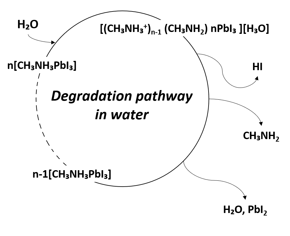
Figure 3. Degradation pathway of metal-organic halide perovskite materials in water.
|
CH₃NH₃PbI₃ (s) → CH₃NH₃PbI (aq) + PbI2 (s) |
(3) |
|
CH₃NH₃PbI (aq) → CH₃NH2 (aq) + HI (aq) |
(4) |
|
4HI (aq) + O2 (g) → 2I2 (s) + 2H2O (l) |
(5) |
|
2HI (aq) → H2 (g) + I2 (s) |
(6) |
In fact, perovskite readily transforms to monohydrate phase MAPbI3∙H2O in moderate humidity (RH < 60%), and to dihydrate phase (MA)4PbI6∙2H2O in high humidity (RH > 80%). This can be explained by the fact that the hydrogen bonding interaction between the lead iodide framework and organic MA+ cations is weakened by hydration. As a result, MA is diffused and detached from PbI6 octahedra, whereby MAPbI3 degrades rapidly. The activation barrier for vacancy-mediated MA+ migration is reduced from 1.18 eV for MAPbI3 to 0.38 eV for water-intercalation, and 1.14 eV for the monohydrated phase. When MAPbI3 is exposed to an aqueous solution, it degrades to PbI2 precipitate, iodide anion, and methylammonium cation [45][46].
Kye et al. [45] identified perovskite degradation in water through a point defect process by density-functional theory (DFT) calculation. Due to the kinetic barrier for I−, ion migration becomes very low when hydrated, and VPbI2 formation occurs spontaneously. In the hydrous compound, the formation of VI and VMA is preferred to the formation of VMAI, so that during the MAPbI3 degradation, the formation of I2 or CH3NH2 or HI is higher than that of MAI (Figure 4a). Unlike bulk MAPbI3, all vacancy defects form deep transition levels through electrostatic interaction with water molecules (Figure 4b).
Several methods have been identified to reduce the degradation of perovskite solar cells (PSC) by water. The first is to add a thin blocking layer like Al2O3 between the perovskite and hole transporting material (HTM) [47][48]. The second is to use moisture blocking HTM. The last method is to use hydrophobic carbon electrode [49][50].
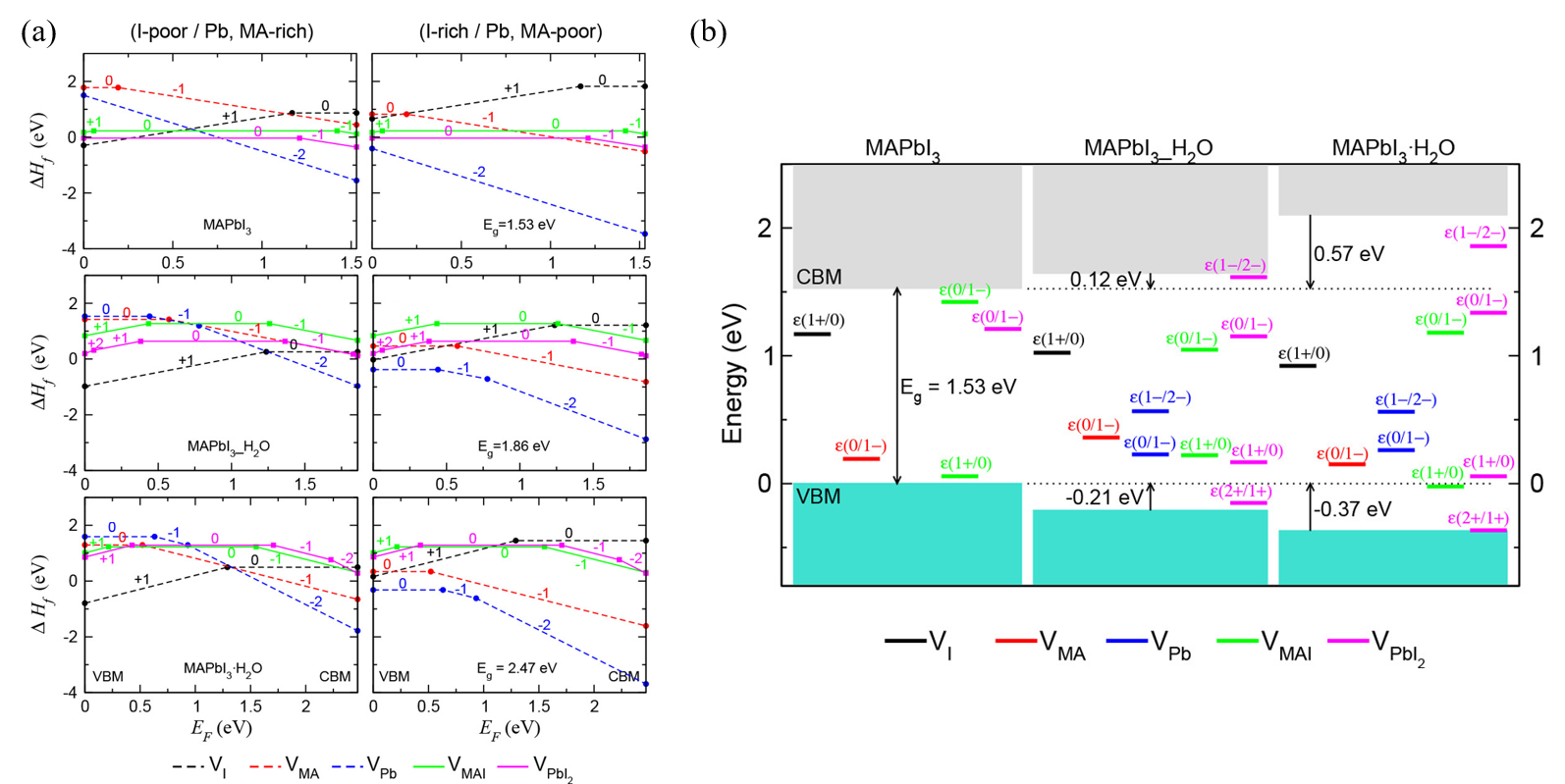
Figure 4. DFT calculation of perovskite’s degradation pathway in water. (a) Formation enthalpies of vacancy point and pair defects as a function of the Fermi energy (EF) under I-poor (Pb-, MA-rich) conditions (left) and I-rich (Pb-, MA-poor) conditions (right). (b) Band alignment and thermodynamic transition levels in MAPbI3, water-intercalated MAPbI3_H2O, and monohydrate MAPbI3·H2O, where deep-lying Pb 5d levels are used as a reference for the VBM and CBM of each phase [45].
Principle of Photoelectrochemical Water Splitting Reaction
The electrochemical reaction is based on the junction of the electrode and the electrolyte. In electrochemical water splitting, a hydrogen evolution reaction (HER) occurs at the cathode, and an oxygen evolution reaction (OER) occurs at the anode. The oxidation and reduction reactions for water splitting are as follows.
|
2H2O + 2e−→H2(g) + 2OH−, Eo = 0.00 V (HER) |
(1) |
|
2OH−→1/2 O2(g) + H2O + 2e−, E = 1.23 V (OER) |
(2) |
The theoretical potential required for electrochemical water splitting is 1.23 V. However, due to the activation energy required for the reaction, more than 1.23 V is required in practice. In other words, the actual response requires a theoretical value of 1.23 V or higher. The additional potential required is called “overpotential”. Researchers are continuously endeavoring to reduce the overpotential [51][52].
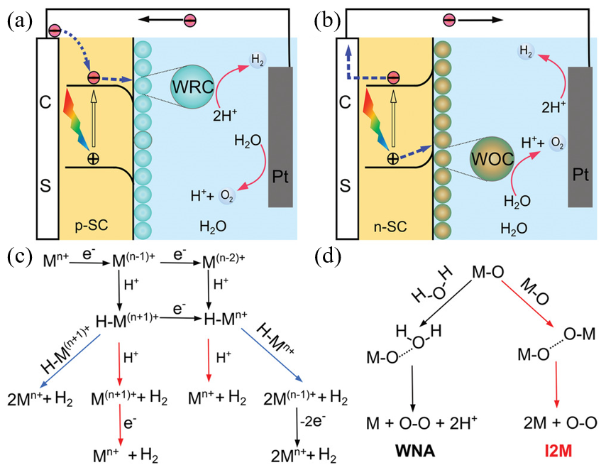
The mechanism by which photoelectrochemical water splitting occurs is shown in Figure 5. Minority carriers generated by semiconductor light absorption are induced into the solution by the electric field at the junction. The electrons and holes generated by the semiconductor are transferred to the molecular catalyst to induce the OER and HER reactions, where, typically, p-type semiconductors are used for water reduction and n-type semiconductors are used for water oxidation. Water reduction is caused by one or two electron steps at the metal center Mn+, which is followed by the reduction of Mn+ and, subsequently, followed by protonation, to give an intermediate hydride. Monometallic and bimetallic pathways occur independently or in parallel, and depend on the catalyst properties, its reduction potential, pKa for deprotonation, and pH. In water oxidation, O–O-forming mechanisms are induced by the interaction between two M–O groups (I2 M) or nucleophilic attack by water (WNA). I2 M mechanisms are achieved by reductive coupling and reductive removal, or by radical coupling through inner/intramolecular pathways. In the WNA mechanism, when the M–O is sufficiently electrophilic, the water molecules attack the M–O to form O–O bonding [53][54][55].
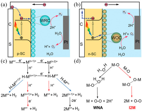
Figure 5. Photoelectrochemical processes involved in (a) water reduction and (b) water oxidation. (c) Proposed mechanistic pathways for H2 generation at a metal center of Mn+. (d) Two mechanistic pathways to form an O–O bond for the molecular catalysts. (ref. [55]).
Mechanism of Perovskite-based PEC Cells
The perovskite photoelectrochemical cell consists of a perovskite light absorption layer, an electron transporting layer, and a hole transporting layer (HTL) to extract the generated electron and hole, and a passivation layer to prevent perovskite degradation in aqueous solution. A simplified working principle of the device may be described as follows: when the light falls on the device, the perovskite layer absorbs the light and generates excitons. The electron and hole pairs (EHPs) are created by the thermal energy, which is diffused and separated through the electron and hole transporting layer, respectively [56]. The performance of the perovskite-based device is influenced by the diffusion length, lifetime, and mobility of the generated carriers. The diffusion length of the perovskite depends on the qualities such as the crystallinity and grain size of the perovskite film, indicating that the diffusion length varies based on the perovskite preparation method. In the case of MAPbI3, as the diffusion length of the hole is longer than that of the electron, mesoporous TiO2 is used to compensate for this short electron diffusion length. Furthermore, performance is improved when the injected charge mobility is fast. Therefore, designing the charge transporting materials and thickness in consideration of the diffusion length and mobility of the charge is one way to improve performance [57][58][59].
The basic function of the electron transporting layer is to enhance the transport of photo-generated electrons through electron-selective contact with the perovskite layer and to prevent hole injection, so as to improve carrier separation and reduce recombination. Generally, TiO2, ZnO, [6,6]-phenyl-C61-butyric acid methyl ester (PCBM), etc. are used as electron transporting materials. Though TiO2 is the most commonly used inorganic electron transporting layer (ETL) material and its electron injection rate is very fast, it has limitations, as recombination occurs due to low electron mobility [60][61][62]. While ZnO has higher electron mobility than TiO2 (Bulk mobility: 205–300 cm2 V−1 s−1), its chemical instability is a drawback [63][64]. PCBM is a conductive polymer material with low photocurrent hysteresis and high short circuit current density. PCBM plays a critical role in improving the quality of the light-absorbing layer by filling the pinholes and vacancies between perovskite grains, resulting in a film with large grains and fewer grain boundaries [65][66][67].
The main function of the hole transporting layer is to improve electron-hole pairs separation by collecting and transporting the generated hole from the perovskite layer. The material used for the hole transporting layer is spiro-OMeTAD, poly (3,4-ethylene dioxythiophene) polystyrene sulfonate (PEDOT:PSS), and CuI. Although Spiro-OMeTAD is one of the best performing HTL materials, its cost can be an impediment, and it is also a small molecule substance which diffuses well into perovskite [68][69]. PEDOT:PSS also exhibits good performance and is a conductive polymer material like PCBM. Alternatively, while CuI has about five times the hole mobility of spiro-OMeTAD and a relatively large particle size, signifying that it does not readily diffuse into the perovskite layer, its shortcomings are that the surface is rough and it is not well bonded with perovskite due to the large particles [70][71].
Perovskite-based device configuration is derived from the dye-sensitized solar cell, and is classified into two types. One of them comprises the transparent conductive substrate coated with the electron transporting material (mesoporous/planar n-type material) under the perovskite layer and hole transporting layer (p-type material) deposited on the perovskite layer. This configuration, which is called n–i–p type, strives for an oxygen evolution reaction. In n–i–p type devices, electron-hole pairs (EHPs) generated in the perovskite layer are transported by the electron transporting material to the transparent conductive oxide (TCO) substrate, and through the hole transporting material, the holes are transported to the metal electrode (Figure 6a). Holes that reach the metal electrode through this mechanism react with oxygen ions to produce oxygen. The other common configuration is inverted compared to the former, and the transparent conductive substrate is coated with the hole transporting material, followed by the perovskite layer and electron transporting layer. This configuration, which is called p–i–n type, strives for a hydrogen evolution reaction. In the p–i–n type perovskite photoelectrochemical cell, a hydrogen evolution reaction occurs by moving electron-hole pairs (EHPs) in a converse mechanism to that of n–i–p type perovskite PEC devices. The EHPs generated in the perovskite layer are transported by the hole transporting material to the TCO substrate, and through the electron transporting material, the electrons are transported to the metal electrode (Figure 6b). The electrons are transported to the metal electrode to produce hydrogen through the reaction with the electrolyte.
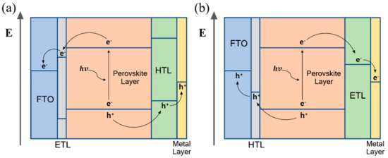
Figure 6. The operating mechanism of perovskite-based photoelectrochemical device (a) n–i–p configuration, (b) p–i–n configuration.
This entry is adapted from the peer-reviewed paper 10.3390/ma13010210
References
- Jovana V. Milić; Jeong‐Hyeok Im; Dominik J. Kubicki; Amita Ummadisingu; Ji‐Youn Seo; Yang Li; Marco A. Ruiz‐Preciado; M. Ibrahim Dar; Shaik M. Zakeeruddin; Lyndon Emsley; et al. Supramolecular Engineering for Formamidinium‐Based Layered 2D Perovskite Solar Cells: Structural Complexity and Dynamics Revealed by Solid‐State NMR Spectroscopy. Advanced Energy Materials 2019, 9, 1900284, 10.1002/aenm.201900284.
- KevinL. Bray; Properties and Applications of Perovskite-Type Oxides.. Chemical Engineering Science 1994, 49, 3337, 10.1016/0009-2509(94)85001-1.
- M. A. Peña; J. L. G. Fierro; Chemical Structures and Performance of Perovskite Oxides. Chemical Reviews 2001, 101, 1981-2018, 10.1021/cr980129f.
- Zhi-Kuang Tan; Reza Saberi Moghaddam; May Ling Lai; Pablo Docampo; Ruben Higler; Felix Deschler; Michael Price; Aditya Sadhanala; Luis M. Pazos; Dan Credgington; et al. Bright light-emitting diodes based on organometal halide perovskite. Nature Nanotechnology 2014, 9, 687-692, 10.1038/nnano.2014.149.
- Zhen Li; Mengjin Yang; Ji-Sang Park; Su-Huai Wei; Joseph J. Berry; Kai Zhu; Stabilizing Perovskite Structures by Tuning Tolerance Factor: Formation of Formamidinium and Cesium Lead Iodide Solid-State Alloys. Chemistry of Materials 2015, 28, 284-292, 10.1021/acs.chemmater.5b04107.
- Kenichiro Tanaka; Takayuki Takahashi; Takuma Ban; Takashi Kondo; Kazuhito Uchida; Noboru Miura; Comparative study on the excitons in lead-halide-based perovskite-type crystals CH3NH3PbBr3 CH3NH3PbI3. Solid State Communications 2003, 127, 619-623, 10.1016/s0038-1098(03)00566-0.
- Kewei Wu; Ashok Bera; Chun Ma; Yuanmin Du; Yang Yang; Liang Li; Tom Wu; Temperature-dependent excitonic photoluminescence of hybrid organometal halide perovskite films. Physical Chemistry Chemical Physics 2014, 16, 22476-22481, 10.1039/c4cp03573a.
- In Chung; Jung-Hwan Song; Jino Im; John Androulakis; Christos D. Malliakas; Hao Li; Arthur J. Freeman; John T. Kenney; Mercouri G. Kanatzidis; ChemInform Abstract: CsSnI3: Semiconductor or Metal? High Electrical Conductivity and Strong Near-Infrared Photoluminescence from a Single Material. High Hole Mobility and Phase-Transitions.. ChemInform 2012, 43, 8579-8587, 10.1002/chin.201237007.
- Adrian P. Goodey; Sarah M. Eichfeld; Kok-Keong Lew; Joan M. Redwing; Thomas E. Mallouk; Silicon Nanowire Array Photoelectrochemical Cells. Journal of the American Chemical Society 2007, 129, 12344-12345, 10.1021/ja073125d.
- Giles Eperon; Samuel D. Stranks; Christopher Menelaou; Michael B. Johnston; Laura Herz; Henry J. Snaith; Formamidinium lead trihalide: a broadly tunable perovskite for efficient planar heterojunction solar cells. Energy & Environmental Science 2014, 7, 982, 10.1039/c3ee43822h.
- Feng Zhang; Haizheng Zhong; Cheng Chen; Xian-Gang Wu; Xiangmin Hu; Hailong Huang; Junbo Han; Bingsuo Zou; Yuping Dong; Brightly Luminescent and Color-Tunable Colloidal CH3NH3PbX3 (X = Br, I, Cl) Quantum Dots: Potential Alternatives for Display Technology. ACS Nano 2015, 9, 4533-4542, 10.1021/acsnano.5b01154.
- Chog Barugkin; Jinjin Cong; The Duong; Shakir Rahman; Hieu T. Nguyen; Daniel Macdonald; Thomas P. White; Kylie R. Catchpole; Ultralow Absorption Coefficient and Temperature Dependence of Radiative Recombination of CH3NH3PbI3 Perovskite from Photoluminescence. The Journal of Physical Chemistry Letters 2015, 6, 767-772, 10.1021/acs.jpclett.5b00044.
- Maria Isabel Alonso; Bethan Charles; Adrián Francisco-López; Miquel Garriga; Mark T. Weller; Alejandro R. Goñi; Spectroscopic ellipsometry study of FAxMA1−xPbI3 hybrid perovskite single crystals. Journal of Vacuum Science & Technology B 2019, 37, 062901, 10.1116/1.5121604.
- Ashwith Chilvery; Sanjib Das; Padmaja Guggilla; Christina Brantley; Anderson Sunda-Meya; A perspective on the recent progress in solution-processed methods for highly efficient perovskite solar cells. Science and Technology of Advanced Materials 2016, 17, 650-658, 10.1080/14686996.2016.1226120.
- Martin A. Green; Anita Ho-Baillie; Henry J. Snaith; The emergence of perovskite solar cells. Nature Photonics 2014, 8, 506-514, 10.1038/nphoton.2014.134.
- David B. Mitzi; Synthesis, Structure, and Properties of Organic-Inorganic Perovskites and Related Materials. Progress in Inorganic Chemistry 2007, 48, 1-121, 10.1002/9780470166499.ch1.
- Gregor Kieslich; Shijing Sun; Anthony K. Cheetham; An extended Tolerance Factor approach for organic–inorganic perovskites. Chemical Science 2015, 6, 3430-3433, 10.1039/c5sc00961h.
- W. Travis; E. N. K. Glover; H. Bronstein; D. O. Scanlon; R. G. Palgrave; On the application of the tolerance factor to inorganic and hybrid halide perovskites: a revised system† †Electronic supplementary information (ESI) available: Lists of metal–anion bond lengths, ABX3 compounds. See DOI: 10.1039/c5sc04845a. Chemical Science 2016, 7, 4548-4556, 10.1039/c5sc04845a.
- Ian M. Reaney; Enrico L. Colla; Nava Setter; Dielectric and Structural Characteristics of Ba- and Sr-based Complex Perovskites as a Function of Tolerance Factor. Japanese Journal of Applied Physics 1994, 33, 3984-3990, 10.1143/jjap.33.3984.
- Teck Ming Koh; Kunwu Fu; Yanan Fang; Shi Chen; T. C. Sum; Nripan Mathews; Subodh G. Mhaisalkar; Pablo P. Boix; Tom Baikie; Formamidinium-Containing Metal-Halide: An Alternative Material for Near-IR Absorption Perovskite Solar Cells. The Journal of Physical Chemistry C 2013, 118, 16458-16462, 10.1021/jp411112k.
- Constantinos C. Stoumpos; Christos D. Malliakas; Mercouri G. Kanatzidis; Semiconducting Tin and Lead Iodide Perovskites with Organic Cations: Phase Transitions, High Mobilities, and Near-Infrared Photoluminescent Properties. Inorganic Chemistry 2013, 52, 9019-9038, 10.1021/ic401215x.
- James M. Ball; Michael M. Lee; Andrew Hey; Henry J. Snaith; Low-temperature processed meso-superstructured to thin-film perovskite solar cells. Energy & Environmental Science 2013, 6, 1739, 10.1039/c3ee40810h.
- James M. Ball; Michael M. Lee; Andrew Hey; Henry J. Snaith; Low-temperature processed meso-superstructured to thin-film perovskite solar cells. Energy & Environmental Science 2013, 6, 1739, 10.1039/c3ee40810h.
- Nobuaki Kitazawa; Y. Watanabe; Y. Nakamura; Optical properties of CH3NH3PbX3 (X = halogen) and their mixed-halide crystals. Journal of Materials Science 2002, 37, 3585-3587, 10.1023/a:1016584519829.
- Fengrui Hu; Huichao Zhang; Chun Sun; Chunyang Yin; Bihu Lv; Chunfeng Zhang; William W. Yu; Xiaoyong Wang; Yu Zhang; Min Xiao; et al. Superior Optical Properties of Perovskite Nanocrystals as Single Photon Emitters. ACS Nano 2015, 9, 12410-12416, 10.1021/acsnano.5b05769.
- Valerio D’Innocenzo; Giulia Grancini; Marcelo J. P. Alcocer; Ajay Ram Srimath Kandada; Samuel D. Stranks; Michael M. Lee; Guglielmo Lanzani; Henry J. Snaith; Annamaria Petrozza; Excitons versus free charges in organo-lead tri-halide perovskites. Nature Communications 2014, 5, 3586, 10.1038/ncomms4586.
- Lung-Chien Chen; Jia-Ren Wu; Zhong-Liang Tseng; Cheng-Chiang Chen; Sheng Hsiung Chang; Jun-Kai Huang; King-Lien Lee; Hsin Ming Cheng; Annealing Effect on (FAPbI3)1−x(MAPbBr3)x Perovskite Films in Inverted-Type Perovskite Solar Cells. Materials 2016, 9, 747, 10.3390/ma9090747.
- Valerio D’Innocenzo; Ajay Ram Srimath Kandada; Michele De Bastiani; Marina Gandini; Annamaria Petrozza; Tuning the Light Emission Properties by Band Gap Engineering in Hybrid Lead Halide Perovskite. Journal of the American Chemical Society 2014, 136, 17730-17733, 10.1021/ja511198f.
- Qingfeng Dong; Yanjun Fang; Yuchuan Shao; Padhraic Mulligan; Jie Qiu; Lei Cao; Jinsong Huang; Electron-hole diffusion lengths > 175 μm in solution-grown CH3NH3PbI3single crystals. Science 2015, 347, 967-970, 10.1126/science.aaa5760.
- QiFeng Han; Sang‐Hoon Bae; Pengyu Sun; Yao‐Tsung Hsieh; Yang (Michael) Yang; You Seung Rim; Hongxiang Zhao; Qi Chen; Wangzhou Shi; Gang Li; et al. Single Crystal Formamidinium Lead Iodide (FAPbI 3 ): Insight into the Structural, Optical, and Electrical Properties. Advanced Materials 2016, 28, 2253-2258, 10.1002/adma.201505002.
- Dong Shi; V. Adinolfi; Riccardo Comin; M. Yuan; Erkki Alarousu; A. Buin; Y. Chen; S. Hoogland; A. Rothenberger; K. Katsiev; et al. Low trap-state density and long carrier diffusion in organolead trihalide perovskite single crystals. Science 2015, 347, 519-522, 10.1126/science.aaa2725.
- Dong Shi; V. Adinolfi; Riccardo Comin; M. Yuan; Erkki Alarousu; A. Buin; Y. Chen; S. Hoogland; A. Rothenberger; K. Katsiev; et al. Low trap-state density and long carrier diffusion in organolead trihalide perovskite single crystals. Science 2015, 347, 519-522, 10.1126/science.aaa2725.
- 10. Galkowski, K.; Mitioglu, A.; Miyata, A.; Plochocka, P.; Portugall, O.; Eperon, G.E.; Wang, J.T.-W.; Stergiopoulos, T.; Stranks, S.D.; Snaith, H.J.; et al. Determination of the Exciton Binding Energy and Effective Masses for Methylammonium and Formamidinium Lead Tri-Halide Perovskite Semiconductors. Energy Environ. Sci. 2016, 9, 962-970, 10.1039/C5EE03435C.
- Rebecca L. Milot; Giles E. Eperon; Henry J. Snaith; Michael B. Johnston; Laura M. Herz; Temperature-Dependent Charge-Carrier Dynamics in CH3NH3PbI3Perovskite Thin Films. Advanced Functional Materials 2015, 25, 6218-6227, 10.1002/adfm.201502340.
- Hikaru Oga; Akinori Saeki; Yuhei Ogomi; Shuzi Hayase; Shu Seki; Correction to Improved Understanding of the Electronic and Energetic Landscapes of Perovskite Solar Cells: High Local Charge Carrier Mobility, Reduced Recombination, and Extremely Shallow Traps. Journal of the American Chemical Society 2014, 136, 16948-16948, 10.1021/ja511140k.
- Christian Wehrenfennig; Giles E Eperon; Michael B Johnston; Henry J Snaith; Laura M Herz; High charge carrier mobilities and lifetimes in organolead trihalide perovskites.. Advanced Materials 2014, 26, 1584-1589, .
- Carlito S. Ponseca; Tom J. Savenije; Mohamed Abdellah; Kaibo Zheng; Arkady Yartsev; Tobjörn Pascher; Tobias C. B. Harlang; Pavel Chábera; Tõnu Pullerits; Andrey Stepanov; et al. Organometal Halide Perovskite Solar Cell Materials Rationalized: Ultrafast Charge Generation, High and Microsecond-Long Balanced Mobilities, and Slow Recombination. Journal of the American Chemical Society 2014, 136, 5189-5192, 10.1021/ja412583t.
- Bo Zhang; Ming-Jia Zhang; Shu-Ping Pang; Chang-Shui Huang; Zhong-Min Zhou; Ng Wang; Ning Wang; Guang-Lei Cui; Ning Wang And; Carrier Transport in CH3NH3PbI3Films with Different Thickness for Perovskite Solar Cells. Advanced Materials Interfaces 2016, 3, 1600327, 10.1002/admi.201600327.
- Hui-Seon Kim; Jin-Wook Lee; Natalia Yantara; Pablo P. Boix; Sneha A. Kulkarni; Subodh Mhaisalkar; Michael Grätzel; Nam-Gyu Park; High Efficiency Solid-State Sensitized Solar Cell-Based on Submicrometer Rutile TiO2 Nanorod and CH3NH3PbI3 Perovskite Sensitizer. Nano Letters 2013, 13, 2412-2417, 10.1021/nl400286w.
- Juan-Pablo Correa-Baena; Miguel Anaya; Gabriel Lozano; Wolfgang Tress; Konrad Domanski; Michael Saliba; Taisuke Matsui; Tor Jesper Jacobsson; Mauricio E. Calvo; Antonio Abate; et al. Unbroken Perovskite: Interplay of Morphology, Electro-optical Properties, and Ionic Movement. Advanced Materials 2016, 28, 5031-5037, 10.1002/adma.201600624.
- Zhicai He; Chengmei Zhong; Xun Huang; Wai-Yeung Wong; HongBin Wu; Liwei Chen; Shijian Su; Yong Cao; Simultaneous Enhancement of Open-Circuit Voltage, Short-Circuit Current Density, and Fill Factor in Polymer Solar Cells. Advanced Materials 2011, 23, 4636-4643, 10.1002/adma.201103006.
- Belen Suarez; Victoria Gonzalez-Pedro; Teresa S. Ripolles; Rafael Sánchez Sánchez; Luis Otero; Ivan Mora-Sero; Recombination Study of Combined Halides (Cl, Br, I) Perovskite Solar Cells. The Journal of Physical Chemistry Letters 2014, 5, 1628-1635, 10.1021/jz5006797.
- Jeffrey A. Christians; Pierre A. Miranda Herrera; Prashant V. Kamat; Transformation of the Excited State and Photovoltaic Efficiency of CH3NH3PbI3Perovskite upon Controlled Exposure to Humidified Air. Journal of the American Chemical Society 2015, 137, 1530-1538, 10.1021/ja511132a.
- 91. Leijtens, T.; Eperon, G.E.; Noel, N.K.; Habisreutinger, S.N.; Petrozza, A.; Snaith, H.J.; Stability of Metal Halide Perovskite Solar Cells. Adv. Energy Mater. 2015, 5, 1500963, 10.1002/aenm.201500963.
- Yun-Hyok Kye; Chol-Jun Yu; Un-Gi Jong; Yue Chen; Aron Walsh; Critical Role of Water in Defect Aggregation and Chemical Degradation of Perovskite Solar Cells. The Journal of Physical Chemistry Letters 2018, 9, 2196-2201, 10.1021/acs.jpclett.8b00406.
- Sunghak Park; Woo Je Chang; Chan Woo Lee; Sangbaek Park; Hyo-Yong Ahn; Ki Tae Nam; Photocatalytic hydrogen generation from hydriodic acid using methylammonium lead iodide in dynamic equilibrium with aqueous solution. Nature Energy 2016, 2, 16185, 10.1038/nenergy.2016.185.
- Simone Guarnera; Antonio Abate; Wei Zhang; Jamie M. Foster; Giles Richardson; Annamaria Petrozza; Henry J. Snaith; Improving the Long-Term Stability of Perovskite Solar Cells with a Porous Al2O3 Buffer Layer. The Journal of Physical Chemistry Letters 2015, 6, 432-437, 10.1021/jz502703p.
- Xu Dong; Xiang Fang; Minghang Lv; Bencai Lin; Shuai Zhang; Jianning Ding; Ningyi Yuan; Improvement of the humidity stability of organic–inorganic perovskite solar cells using ultrathin Al2O3layers prepared by atomic layer deposition. Journal of Materials Chemistry A 2015, 3, 5360-5367, 10.1039/c4ta06128d.
- Jian Liu; Yongzhen Wu; Chuanjiang Qin; Xudong Yang; Takeshi Yasuda; Ashraful Islam; Kun Zhang; Wenqin Peng; Wei Chen; Liyuan Han; et al. A dopant-free hole-transporting material for efficient and stable perovskite solar cells. Energy & Environmental Science 2014, 7, 2963-2967, 10.1039/c4ee01589d.
- Anyi Mei; Xiong Li; Linfeng Liu; Zhiliang Ku; Tongfa Liu; Yaoguang Rong; M. Xu; Min Hu; Jiangzhao Chen; Ying Yang; et al. A hole-conductor-free, fully printable mesoscopic perovskite solar cell with high stability. Science 2014, 345, 295-298, 10.1126/science.1254763.
- Uk Sim; Hui-Yun Jeong; Tae-Youl Yang; Ki Tae Nam; Nanostructural dependence of hydrogen production in silicon photocathodes. Journal of Materials Chemistry A 2013, 1, 5414, 10.1039/c3ta00048f.
- Yongwen Tan; Hao Wang; Pan Liu; Yuhao Shen; Chun Cheng; Akihiko Hirata; Takeshi Fujita; Zheng Tang; Mingwei Chen; Versatile nanoporous bimetallic phosphides towards electrochemical water splitting. Energy & Environmental Science 2016, 9, 2257-2261, 10.1039/c6ee01109h.
- Serena Berardi; Samuel Drouet; Laia Francás; Carolina Gimbert-Suriñach; Miguel Guttentag; Craig Richmond; Thibaut Stoll; Antoni Llobet; Molecular artificial photosynthesis. Chemical Society Reviews 2014, 43, 7501-7519, 10.1039/c3cs60405e.
- Arianna Savini; Paola Belanzoni; Gianfranco Bellachioma; Cristiano Zuccaccia; Daniele Zuccaccia; Alceo Macchioni; Activity and degradation pathways of pentamethyl-cyclopentadienyl-iridium catalysts for water oxidation. Green Chemistry 2011, 13, 3360, 10.1039/c1gc15899f.
- Fujun Niu; Degao Wang; Fei Li; Yanming Liu; Shaohua Shen; Thomas J. Meyer; Hybrid Photoelectrochemical Water Splitting Systems: From Interface Design to System Assembly. Advanced Energy Materials 2019, 1900399, 1-24, 10.1002/aenm.201900399.
- Pablo P. Boix; Kazuteru Nonomura; Nripan Mathews; Subodh G. Mhaisalkar; Current progress and future perspectives for organic/inorganic perovskite solar cells. Materials Today 2014, 17, 16-23, 10.1016/j.mattod.2013.12.002.
- Baicheng Weng; Corey R. Grice; Jie Ge; Tilak Poudel; Xunming Deng; Yanfa Yan; Barium Bismuth Niobate Double Perovskite/Tungsten Oxide Nanosheet Photoanode for High-Performance Photoelectrochemical Water Splitting. Advanced Energy Materials 2017, 8, 1701655, 10.1002/aenm.201701655.
- Tze Chien Sum; Nripan Mathews; Advancements in perovskite solar cells: photophysics behind the photovoltaics. Energy & Environmental Science 2014, 7, 2518-2534, 10.1039/c4ee00673a.
- Rui Liu; Zhi Zheng; Joshua Spurgeon; Xiaogang Yang; Enhanced photoelectrochemical water-splitting performance of semiconductors by surface passivation layers. Energy & Environmental Science 2014, 7, 2504-2517, 10.1039/c4ee00450g.
- Tomas Leijtens; Giles E. Eperon; Sandeep Pathak; Antonio Abate; Michael M. Lee; Henry J. Snaith; Overcoming ultraviolet light instability of sensitized TiO2 with meso-superstructured organometal tri-halide perovskite solar cells. Nature Communications 2013, 4, 2885, 10.1038/ncomms3885.
- Gerrit Boschloo; Donald Fitzmaurice; Spectroelectrochemical Investigation of Surface States in Nanostructured TiO2Electrodes. The Journal of Physical Chemistry B 1999, 103, 2228-2231, 10.1021/jp984414e.
- Jongmin Choi; Seulki Song; Maximilian T. Hörantner; Henry J. Snaith; Taiho Park; Well-Defined Nanostructured, Single-Crystalline TiO2 Electron Transport Layer for Efficient Planar Perovskite Solar Cells. ACS Nano 2016, 10, 6029-6036, 10.1021/acsnano.6b01575.
- Yanming Sun; Jung Hwa Seo; Christopher J. Takacs; Jason Seifter; Alan J. Heeger; Inverted Polymer Solar Cells Integrated with a Low-Temperature-Annealed Sol-Gel-Derived ZnO Film as an Electron Transport Layer. Advanced Materials 2011, 23, 1679-1683, 10.1002/adma.201004301.
- Shuyan Shao; Kaibo Zheng; Tõnu Pullerits; Fengling Zhang; Enhanced Performance of Inverted Polymer Solar Cells by Using Poly(ethylene oxide)-Modified ZnO as an Electron Transport Layer. ACS Applied Materials & Interfaces 2013, 5, 380-385, 10.1021/am302408w.
- Guichuan Xing; Nripan Mathews; Shuangyong Sun; Swee Sien Lim; Yeng Ming Lam; Michael Grätzel; Subodh Mhaisalkar; Tze Chien Sum; Long-Range Balanced Electron- and Hole-Transport Lengths in Organic-Inorganic CH3NH3PbI3. Science 2013, 342, 344-347, 10.1126/science.1243167.
- George Kakavelakis; Temur Maksudov; Dimitrios Konios; Ioannis Paradisanos; George Kioseoglou; Emmanuel Stratakis; Emmanuel Kymakis; Efficient and Highly Air Stable Planar Inverted Perovskite Solar Cells with Reduced Graphene Oxide Doped PCBM Electron Transporting Layer. Advanced Energy Materials 2016, 7, 1602120, 10.1002/aenm.201602120.
- Yang Bai; Hui Yu; Zonglong Zhu; Kui Jiang; Teng Zhang; Ni Zhao; Shihe Yang; He Yan; High performance inverted structure perovskite solar cells based on a PCBM:polystyrene blend electron transport layer. Journal of Materials Chemistry A 2015, 3, 9098-9102, 10.1039/C4TA05309E.
- Francisco Fabregat-Santiago; Juan Bisquert; Le Cevey; Peter Chen; Mingkui Wang; Shaik M. Zakeeruddin; Michael Grätzel; Electron Transport and Recombination in Solid-State Dye Solar Cell with Spiro-OMeTAD as Hole Conductor. Journal of the American Chemical Society 2009, 131, 558-562, 10.1021/ja805850q.
- H. J. Snaith; M. Gratzel; Electron and Hole Transport through Mesoporous TiO2 Infiltrated with Spiro-MeOTAD. Advanced Materials 2007, 19, 3643-3647, 10.1002/adma.200602085.
- Hui Luo; Xuanhuai Lin; Xian Hou; Likun Pan; Sumei Huang; Xiaohong Chen; Efficient and Air-Stable Planar Perovskite Solar Cells Formed on Graphene-Oxide-Modified PEDOT:PSS Hole Transport Layer. Nano-Micro Letters 2017, 9, 39, 10.1007/s40820-017-0140-x.
- Weibo Yan; Yunlong Li; Yu Li; Senyun Ye; Zhiwei Liu; Shufeng Wang; Zuqiang Bian; Chunhui Huang; Stable high-performance hybrid perovskite solar cells with ultrathin polythiophene as hole-transporting layer. Nano Research 2015, 8, 2474-2480, 10.1007/s12274-015-0755-5.

