Germanium (Ge) ion implantation into silicon waveguides will induce lattice defects in the silicon, which can eventually change the crystal silicon into amorphous silicon and increase the refractive index from 3.48 to 3.96. A subsequent annealing process, either by using an external laser or integrated thermal heaters can partially or completely remove those lattice defects and gradually change the amorphous silicon back into the crystalline form and, therefore, reduce the material’s refractive index. In addition, Ge ion implantation and annealing are also demonstrated to enable post-fabrication trimming of ring resonators and Mach–Zehnder interferometers and to implement nonvolatile programmable photonic circuits.
1. Introduction
Silicon photonics is currently a commercially established and yet fast-growing technology for communication systems. It has also started to play a significant role in many other applications, including chemical and biomedical sensing, LiDAR application in driving assistance systems, and in applications for building quantum networks. The integration with III–V light source materials such as indium phosphide through bonding has also been reported to solve the lack of intrinsic light emission within the silicon platform [
1,
2,
3,
4,
5,
6,
7,
8,
9].
To monitor the status of fabrication processes and characterise the performance of photonic circuits after production, wafer-scale testing is an essential technology in a semiconductor production line [
10,
11]. However, testing the silicon photonics devices optically at wafer scales is nontrivial. Various techniques can be used to couple the optical signal from optical fibres to photonic chips, such as prism coupling, butt coupling, end-fire coupling, and grating coupling [
12,
13,
14,
15]. Among them, grating couplers provide an effective coupling technique that can couple between integrated waveguides and the out-of-plane fibres at the wafer scale without dicing the photonic chips [
16,
17]. However, grating couplers are normally only used as the input/output for the whole photonic circuit. Therefore, apart from measuring the performance of the entire circuit during wafer-scale testing, it is not possible to test any subsystems or individual devices on the photonic chips. Once a problem within the circuits, such as a fabrication error, occurs, early identification and analysis can bring huge cost savings. Therefore, it is desirable to routinely test some key sensitive subsystems or individual devices on the photonic chips, at a wafer scale. Erasable grating couplers and directional couplers are, therefore, proposed for such applications, based on germanium (Ge) ion implantation and annealing technologies [
18,
19].
With current semiconductor fabrication technology, the uniformity of the fabrication processes for some silicon photonics devices, such as ring resonators and Mach–Zehnder interferometers (MZIs), exhibits variability. The optical phase error induced by the variation in waveguide dimensions across the chip will significantly change the device performance. This is one of the major factors affecting the yield of final silicon photonic modules in production [
20,
21]. For example, the resonant wavelength and Q factor of ring resonators will be affected by variations in the fabrication process [
22,
23]. The transmission of MZI mainly depends on the phase difference between the two arms, and this will also suffer from the variations in the fabrication process [
24,
25].
Silicon photonic modulators and filters have benefited from the resonance properties of ring resonators. However, this structure is extremely susceptible to fabrication variations [
26]. Several methods have been investigated to tune the resonant wavelength of optical ring resonators. Electron beam and laser irradiation are two techniques that have been used for trimming, with each utilising a different process to realise a refractive index change [
27]. Inducing strain and compaction into an oxide cladding by e-beam can change the effective index of the optical mode in the devices [
28,
29]. The polymethyl methacrylate cladding allows the resonant wavelength of ring resonators to be trimmed after irradiation by ultraviolet light [
30]. Post-fabrication trimming can also be realised by introducing photosensitive materials onto the waveguide surface and subsequently exposing them to lasers [
31]. The optical properties of the waveguide can also be shifted by depositing and partial etching of a thin SiN film on top of devices [
32]. Laser-induced lattice damage can also change the refractive index of silicon waveguides and can provide a shift in resonant wavelength [
33]. Herein demonstrated that Ge ion implantation and annealing can be applied for post-fabrication trimming [
34,
35,
36,
37], with some unique advantages over other techniques, such as a large change in refractive index change and easy implementation.
In addition to the applications of wafer-scale testing and post-fabrication device trimming, herein also implemented a proof of principle of nonvolatile programmable photonic circuits with the Ge implantation technology [
38]. Based on the refractive index change associated with Ge ion implantation and annealing mentioned above, the flow of an optical signal within the photonic circuit can be switched or rerouted using erasable directional couplers or trimmable MZIs. Such devices were used as the basic building blocks for large-scale programmable photonics circuits. After fine-tuning the transmission, the working states of the directional couplers or MZIs are fixed and do not need a continuous electrical power supply to retain the operating point [
34]. This will greatly reduce the power consumption, compared with more traditional programmable photonic circuits, implemented with MZI arrays controlled by integrated thermal heaters [
39].
2. Ion Implantation and Annealing
2.1. Ge Ion Implantation
Ion implantation is a widely used fabrication process to achieve impurity doping in a solid target [
40]. Typically, in the CMOS industry, ions of elements from groups III and V are implanted to change the free carrier concentration. The process to alter the charge density present in the sample via doping is different from the ion implantation process used in this study to change the refractive index of the silicon waveguide via crystal damage. For crystalline silicon waveguides, lattice disorder can be induced during the implantation process. Therefore, the effective index of propagating mode in optical devices can be altered through this process via a damage-induced change in the refractive index. During the implantation process, the ions are accelerated in an electric field and injected into the sample, causing lattice damage in the crystalline silicon. The alteration in the refractive index is attributed directly to this lattice damage [
41,
42]. Therefore, a variety of implanted species can be utilised to cause lattice damage.
In this project, Ge was chosen as the implanted ion in the ion implantation process to create amorphous sections in a crystalline silicon waveguide. Firstly, Ge is a group IV element, which means that the free carrier concentration of the silicon waveguide will not be changed. Secondly, it is a CMOS-compatible element, and compared with carbon and silicon, Ge has a higher relative mass and can cause greater lattice damage than other group IV elements for the same implanted dose [
41,
43]. Consequently, amorphisation can be achieved for a lower dose than for lighter ions. Ion implantation is also a temperature-dependent process. Low ion implantation temperature can reduce the required ion implantation dose and implant time [
42]. However, it also increases the utilisation time of the implantation equipment and production costs because self-heating via the ion beam must be avoided. The lattice disorder in silicon crystal has been reported with a very mild temperature dependency below 323 K [
44]. Therefore, room temperature can be used to reduce fabrication costs.
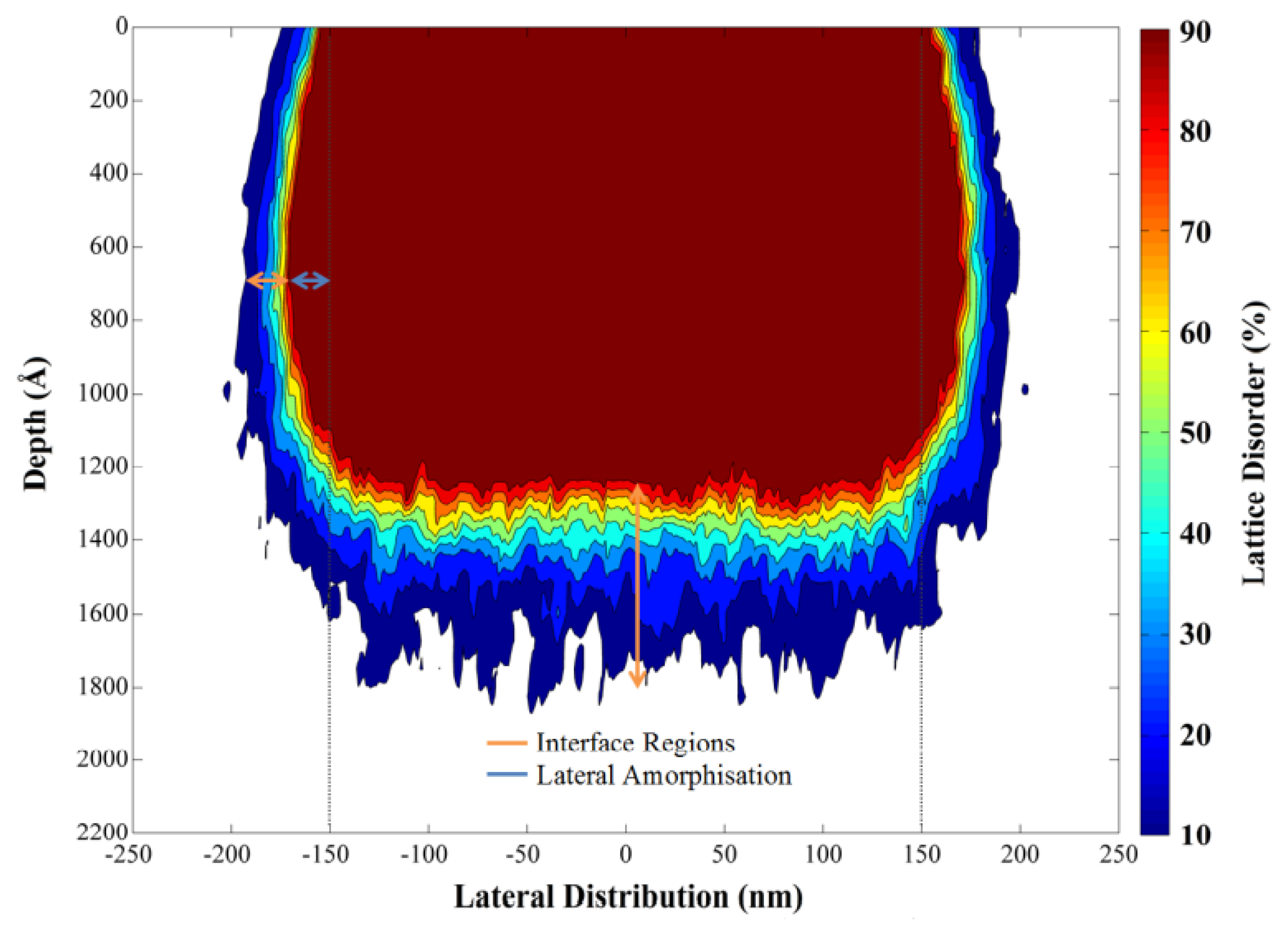
Figure 1 shows the lattice damage profile in a 220 nm thick silicon waveguide [
45]. The King and King 3D software packages were used to simulate the damage profile of silicon waveguides after Ge ion implantation [
46,
47,
48]. The energy and implantation dose in this simulation are 100 keV and 1 × 10
15 ions/cm
2, respectively. The real part of the refractive index of the implanted silicon waveguide regions was increased by approximately 0.5 due to 80% lattice disorder or more, which was taken to be the definition of amorphisation. The induced lattice defects in silicon will also result in a small increase (0.04) of the imaginary part of the refractive index [
49].
3. Applications
The ion implantation technique has been widely reported for modification and doping of materials. The performance of devices can, therefore, be improved after this treatment [
60,
61,
62,
63,
64]. In previous experiments, Ge ion implantation was used to induce lattice damage into crystalline silicon waveguides, and the real part of the refractive index can be increased to approximately 3.96. The implantation process will not generate free carriers in silicon waveguides because, similar to silicon, Ge is a group IV material. The transmission of silicon optical devices can be shifted after the implantation process. This alteration of the performance of optical devices is larger than the typical variation brought about by fabrication errors, therefore allowing for correction or ‘trimming’ of such devices. The annealing process, also widely reported, is the mechanism utilised in removing the lattice defects created by implantation [
65,
66,
67,
68]. Herein used the annealing technique to tune the performance of implanted optical devices for different applications, including wafer-scale testing, post-fabrication trimming, and programmable photonic circuits.
3.1. Wafer-Scale Testing
The traditional testing methods, such as butt coupling, are not suitable for large-scale comprehensive testing. They offer limited opportunities for accessing intermediate testing points in photonic circuits for monitoring individual optical devices within a photonic circuit. One possible solution is to use another device, such as an MZI or directional coupler, to tap a small portion of the optical signal from the testing point in a photonic circuit for monitoring and testing purposes. However, these couplers are not removable and will induce permanent optical loss throughout the operational life of photonic circuits [
59,
69].
On the other hand, our erasable grating couplers and directional couplers were demonstrated to enable flexible comprehensive wafer-scale testing for large-scale integrated photonic circuits without inducing additional loss during subsequent operation of the photonic circuits. The optical signal used for monitoring can be coupled in/out through implanted devices, which can be erased after testing. After the annealing process, the measured residual insertion loss is typically the order of −25 dB for the erasable grating couplers and −18 dB for the erasable directional couplers [
18,
19].
The implanted sections of these devices can be annealed by laser or electrical heaters, with the latter being a more feasible choice for commercial silicon photonic chips with high volume production and large-scale integration, as thermal heaters can be activated even in packaged devices. Tapers with a length of at least 700 μm are required for each erasable grating coupler, to minimise residual loss after annealing and to facilitate straightforward alignment within a commercial wafer prober, whereas erasable directional couplers can be much smaller [
50]. A smaller insertion loss should be potentially achieved if a shorter implanted waveguide is used. Furthermore, there is typically no requirement to launch 90% of an optical signal for testing purposes.
3.2. Post-Fabrication Trimming of Optical Devices
Post-fabrication trimming techniques were investigated to fine-tune the optical phase in waveguide-based devices. In this study, the refractive index of the silicon crystalline waveguide was controlled by introducing implanted sections and annealing technologies. The effective index of a propagating mode and the working performance of devices, including MZIs, ring resonators, and directional couplers could, therefore, be trimmed.
For ring resonators, fabrication tolerances will influence the resonant wavelength, the accuracy of which is essential for applications such as sensing and modulation. In our study, the effective index change of the propagating mode in the ring waveguide depends on the length of the induced implantation section. This induced shift can also be controlled by annealing methods such as laser and integrated thermal heating. Our research also successfully demonstrated post-fabrication trimming of the critical coupling condition for racetrack resonators. To achieve this, the same technique was used to implant the slab layer between and bus waveguide and the ring waveguide. Then, the coupling efficiency could be trimmed through partial annealing of implanted section.
Herein also studied post-fabrication trimming of MZIs using similar techniques. Implanted sections were created in the two arms of MZIs. Then, an annealing process could gradually anneal the implanted waveguide sections and trim the operating point, hence the transmission performance. One example application is for optical modulation, where MZIs can offer the highest modulation efficiency working at the quadrature point.
3.3. Programmable Photonic Circuits
Based on the mature fabrication and integration technologies, photonic circuits can support complex applications. Programmable photonic circuits with application flexibility can be designed and developed to realise a variety of functions with the same chip when programmed in different ways. These circuits are built with waveguide meshes, phase shifters, and tuneable couplers, which can be programmed by software [
39]. The flow of light in the programmable PICs can be electrically manipulated to realise different circuit functionality from the same chip. Conventional programmable circuits use an electrical signal to control integrated heaters to induce thermo-optic effects in thermal phase shifters. However, hundreds of heaters are typically required for such a system, which has also brought new issues into programmable photonics circuits, such as high power consumption, heat dissipation, and crosstalk between each phase shifter.
The erasable and tuneable optical devices investigated in this study can be used to fabricate nonvolatile actuators in programmable photonics circuits. By introducing a section of an implanted waveguide and then controlling annealing, the routing of an optical signal in an implanted MZI or directional coupler can be tuned. There are also other techniques proposed for building nonvolatile programmable circuits, such as phase-change materials [
70,
71] and mechanically latched MEMS [
72,
73]. However, our proposed programmable photonic circuits based on ion implantation and annealing techniques are more CMOS compatible.
4. Conclusions
Herein used Ge ion implantation and annealing technologies to realise erasable and trimmable silicon optical devices, including erasable grating couplers, erasable directional couplers, tuneable MZIs, and ring resonators. The applications of these devices were also discussed.
Erasable grating couplers and directional couplers were demonstrated as flexible testing points used for wafer-scale testing of photonic integrated circuits, which facilitates comprehensive circuit testing. These testing points can then be erased permanently after testing, with negligible residual insertion loss. Our proposed technology was also used in the post-fabrication trimming of silicon photonic devices with many unique advantages. For trimming of ring resonators, a large trimming range, up to 10 nm (across the entire free-spectral range) of 10 µm rings, was achieved. Table 1 illustrates a comparison of the current trimming methods of ring resonators.
Table 1. Comparison of current trimming of ring resonators.
| |
Ref. [29] |
Ref. [30] |
Refs. [74,75] |
Ref. [36] |
| Methods |
E-beam |
UV light |
Sb2Se3 |
Ion implantation and annealing |
CMOS compatibility
of materials |
Yes |
No |
No |
Yes |
| Throughput (minutes/device) |
Low |
Low |
Low |
High |
| (>17) |
(>10) |
(<1) |
(<1) |
| Effective index change |
0.06 |
<0.1 |
0.017 |
0.19 |
For trimming of MZIs, a trimming accuracy of 0.078 rad and a trimming range of 1.2π were achieved with active feedback control. These trimmable and tuneable devices, such as MZIs and directional couplers, were also demonstrated for rerouting the optical signals of a photonic circuit after fabrication. This enabled us to design a multipurpose photonic integrated circuit with the capability to be programmed for various specific applications after fabrication or packaging. This one-time programmable photonic circuit can potentially reduce the overall production costs, with an increase in production volume, and can speed up the development or prototyping cycles for new photonic circuits.
This entry is adapted from the peer-reviewed paper 10.3390/mi13020291