Atomic layer deposition (ALD) of high-κ dielectrics on two-dimensional (2D) materials (including graphene and transition metal dichalcogenides) still represents a challenge due to the lack of out-of-plane bonds on the pristine surfaces of 2D materials, thus making the nucleation process highly disadvantaged. The typical methods to promote the nucleation (i.e., the predeposition of seed layers or the surface activation via chemical treatments) certainly improve the ALD growth but can affect, to some extent, the electronic properties of 2D materials and the interface with high-κ dielectrics. Hence, direct ALD on 2D materials without seed and functionalization layers remains highly desirable. In this context, a crucial role can be played by the interaction with the substrate supporting the 2D membrane. In particular, metallic substrates such as copper or gold have been found to enhance the ALD nucleation of Al2O3 and HfO2 both on monolayer (1 L) graphene and MoS2. Similarly, uniform ALD growth of Al2O3 on the surface of 1 L epitaxial graphene (EG) on SiC (0001) has been ascribed to the peculiar EG/SiC interface properties.
1. Introduction
Two-dimensional (2D) materials such as semi-metallic graphene and the semiconducting transition metal dicalchogenides (TMDs) have been the object of intensive research investigations in the last 15 years due to their wide range of potential applications in electronics, optoelectronics, and sensing. As an example, the excellent carrier mobility (10
3–10
5 cm
2/Vs) [
1] and micrometer electron mean free path [
2] of graphene have been exploited in the demonstration of high-frequency (100–300 GHz) transistors [
3,
4], for which the low on/off current ratio (due to the lack of an energy bandgap) represents a minor issue. On the other hand, semiconducting TMDs (including MoS
2, WS
2, MoSe
2, and WSe
2) are currently regarded as the most suitable channel materials for ultra-thin body field effect transistors to be employed in next-generation logic or switching applications [
5,
6]. As an example, transistors with high on/off current ratios (10
6–10
8) and low subthreshold swings (SS ≈ 70 meV/decade) [
7,
8] have been fabricated using monolayer (1 L) MoS
2 (with a direct bandgap of 1.8 eV) or multilayer MoS
2 (with an indirect bandgap of 1.2 eV) [
9,
10].
Practical implementation of electronic devices based on 2D materials requires their combination with high-κ dielectrics, such as Al
2O
3, HfO
2, and ZrO
2. In the case of top-gated field effect transistors with graphene or MoS
2 channels, high-κ gate insulators are necessary for efficient electrostatic control of the lateral source-to-drain current while minimizing the gate leakage phenomena [
11,
12,
13]. Furthermore, the encapsulation of the monolayer or multilayers of MoS
2 with high-κ dielectrics has been demonstrated to be highly beneficial in the improvement of the field effect mobility up to 200–500 cm
2 V
−1s
−1 due to the efficient reduction of charged impurity scattering [
7,
8,
14]. Obviously, with the scaling down process which invests the electronic field, most of these applications require high-κ dielectrics in the form of uniform and ultra-thin layers. Aside from conventional field effect transistor structures, novel device concepts and architectures also require the integration of high-quality and ultra-thin insulators on the surfaces of 2D materials [
15,
16]. As an example, the recently investigated graphene-base hot electron transistors (GBHETs) for THz electronics require the integration of an ultra-thin insulator on graphene working as a base collector tunnel barrier for vertical transport [
17,
18,
19]. Furthermore, graphene sensors may involve high-κ deposition on graphene as a functional layer toward specific chemical and biological molecules [
20].
2. Atomic Layer Deposition on 2D Materials
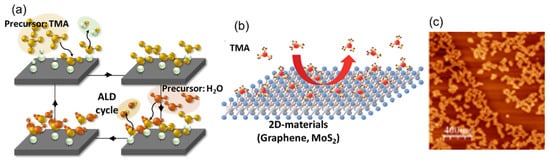
The ALD is the most suitable deposition technique for the growth of ultra-thin and conformal dielectric layers on a substrate. The key strength of ALD is related to its peculiar deposition mechanism. It is based on sequential and self-limited chemical reactions between the properly selected chemical precursors and the active sites of the substrate surface, which results in the so-called layer-by-layer growth mode (see
Figure 1a). This characteristic principle of growth allows for obtaining uniform, conformal, and pinhole-free depositions with angstrom-level control of the thickness in a large area [
31]. However, ALD implementation on a pristine surface of graphene and other 2D materials is a difficult task due to the lack of dangling bonds working as active sites or functional groups for the adsorption of ALD precursors (as depicted in
Figure 1b). The main consequence of this feature is a lack of deposition or the formation of inhomogeneous films (e.g., see the image of ALD-Al
2O
3 on the pristine MoS
2 surface in
Figure 1c).
Figure 1. (
a) Schematic of a typical cycle in ALD growth. (
b) Schematic diagram showing the adsorption and desorption processes of a TMA precursor during the ALD deposition of Al
2O
3 on the 2D materials [
32]. (
c) AFM image of the ALD-Al
2O
3 layer deposited on a pristine MoS
2 surface [
33].
2.1. Methods to Promote ALD Growth on 2D Materials
To date, a wide variety of processes has been reported to promote ALD nucleation on 2D layered materials, which finally results in the deposition of uniform dielectric layers. Table 1 reports a selection of the literature results for different types of 2D materials, with the indication of the used surface activation for ALD, the deposited high-κ insulator, its thickness and uniformity, and eventual damage introduced in the 2D material by the ALD process.
Table 1. ALD deposition of high-κ dielectrics on 2D materials.
| Ref |
2D Material |
ALD Process |
| ALD Activation |
TALD (°C) |
High-κ Type |
Uniformity |
2D Damage |
| |
Seed layer deposition |
|
| [34] |
CVD-graphene on SiO2 |
3,4,9,10-perylene tetracarboxylic acid (PTCA) |
100 °C |
Al2O3, ~2 nm |
High |
Not |
| [35] |
CVD-graphene on SiO2 |
Poly(4-vinylphenol) (PVP) |
------ |
Al2O3, 20 nm |
High |
Not |
| [36] |
CVD-MoS2 and CVD-WS2 |
Perylene bisimide |
80 °C |
Al2O3, ~3 nm |
High |
Not |
| [37] |
Exfoliated graphene |
Evaporated Al |
250 °C |
Al2O3, ~3 nm |
High for seed layer > 1.2 nm |
Not |
| [38,39] |
CVD-MoS2 |
Al |
150 °C |
ZrO2, ~15 nm |
High |
Not |
| [40] |
MoS2 by sulfurization of Mo |
SiO2 nanoparticles |
300 °C |
Al2O3, 5.7 nm
HfO2, 2.8 nm |
High |
Not |
| [41] |
Exfoliated graphene |
Seed layer of H2O-assisted dielectric at low temperature (100 °C) |
100 °C |
Al2O3, ~11 nm |
High |
Not |
| [42] |
Transferred CVD-graphene on SiO2 |
Seed layer of H2O-assisted dielectric at low temperature (100 °C) |
250 °C |
Al2O3, ~22 nm |
High |
Not |
| [43] |
Exfoliated MoS2 |
Seed layer of H2O-assisted dielectric at low temperature (80 °C) |
180°C |
Al2O3, <10 nm |
High |
Not |
| [44] |
Exfoliated WS2 |
Evaporated Al |
95 °C |
HfO2, ~20 nm |
High |
Not |
| |
|
Chemical
functionalization |
|
|
|
|
| [45] |
Exfoliated graphene |
NO2 |
250 °C |
Al2O3, ~12 nm |
High |
Current and mobility degradation |
| [46] |
Exfoliated graphene |
O3 (25–200 °C) |
200 °C |
Al2O3, ~15 nm |
High |
Significant defect amount during O3 treatment at 200 °C |
| [33] |
Exfoliated MoS2 |
O3 (30°) |
200 °C |
Al2O3, ~5 nm |
High |
Not |
| [47,48] |
HOPG |
O3 (25°) |
200 °C |
Al2O3, ~10 nm |
High |
Damage to 2D crystal |
| [49] |
Exfoliated MoSe2, WSe2 |
UV-O3 |
200 °C |
HfO2, ~4 nm |
High on MoSe2
Low on WSe2 |
Partial etching of the 2D layers |
| [50] |
Exfoliated MoS2 |
O2-plasma |
250 °C |
Al2O3, ~10 nm
HfO2, ~10 nm |
High |
MoS2 oxidation |
| [51] |
Transferred CVD-graphene |
O2-plasma |
100 °C |
Al2O3, ~10 nm |
High |
Significant amount of defects |
| [52] |
Exfoliated graphene |
N2-plasma |
------ |
Al2O3, ~28 nm |
High |
Significant amount of defects and reduced conductivity |
| |
|
ALD parameter
tuning |
|
|
|
|
| [53] |
Exfoliated graphene |
Low-temperature ALD process |
80–150 °C |
Al2O3 |
High (98%) at 80 °C |
Not |
| [32] |
Exfoliated MoS2, WS2, WSe2, h-BN |
Low-temperature ALD process |
150 °C |
Al2O3, 1, 10 nm |
Variable as the 2D polarizability (WSe2 < WS2 < MoS2 < h-BN) |
Not |
| [54] |
Exfoliated HOPG and MoS2 |
Low-temperature ALD process |
50 °C |
Al2O3, few nm |
High |
Not |
| [53] |
CVD graphene on Cu |
Long or multiple precursor pulses |
200 °C |
Al2O3, few nm |
Variable |
Not |
From the historical point of view, most of these approaches have been developed for graphene [
35,
37,
55,
56], and many of them have been adapted to other layered materials, such as TMDs [
36]. These processes can be grouped into two categories:
- (i)
-
Predeposition of a seed-layer;
- (ii)
-
Chemical pre-functionalization.
The seed layers can be of both an organic nature, such as self-assembled monolayers (SAM) [
34,
57] or spin-coated polymers layers [
35,
36,
55], and an inorganic nature, such as sputtered or evaporated metal or metal oxide films [
37,
38,
39,
56] or SiO
2 nanoparticles [
40]. They can be pre-deposited “ex situ” (i.e., outside the ALD reactor chamber) and also “in situ” (i.e., within the reactor), like in the case of low temperature H
2O-assisted dielectric seed layer growth on the surface of graphene [
41,
42].
The seed layer approach proved to be an efficient and widely used method to promote the subsequent ALD growth process on graphene and TMDs. Typically, the spin-coating, self-assembling, and physical deposition methods (e.g., evaporation) used to deposit seed layers result in limited damage to the 2D membranes. However, from the electrical point of view, poor interface quality between the seed layer and 2D materials can result in a high-density interface or near-interface traps, ultimately compromising the performances of the final device. On the other hand, the metal seed layer deposition has been found to be beneficial for protecting the structural and electrical properties of the 2D material from the following ALD process. In particular, recent reports on the ALD deposition of ZrO
2 on MoS
2 [
38,
39] demonstrated that the Al seed layer reduces the oxidation effect of the 2D material by the co-reactant (H
2O, O
3) during the ALD process, mainly for the O
3-based method. Moreover, the introduction of a seed layer limits the minimum achievable thickness of the high-κ film, and this can represent a serious concern for the downscaling of 2D material-based transistors.
Chemical pretreatments of a 2D material surface, such as exposure to NO
2 [
45], O
3 [
33,
46,
47,
48] or O
2-plasma [
50,
51], and N
2-plasma [
52], introduce functional groups or dangling bonds, enabling the ALD nucleation and growth of high-κ dielectrics. These approaches allow, in principle, the growth of ultra-thin insulating films, but at the same time, they can introduce defects in the 2D layer, degrading its electronic properties.
Aside from the seeding layer and chemical pretreatments, the ALD process conditions (e.g., the deposition temperature and the pulse and purge times) can play a key role in achieving uniform coverage of a 2D material’s surface. ALD depositions of Al
2O
3 or HfO
2 are typically carried out in a temperature window from 200 to 300 °C, which ensures the optimal reaction of the precursors. However, lower deposition temperatures allow higher physisorption of the precursors on the graphene or TMD surface, improving ALD nucleation [
32,
41,
53]. As an example, Aria et al. [
53] demonstrated improved coverage and uniformity of deposited films on graphene within a temperature window of 80–100 °C for both Al
2O
3 and HfO
2 materials. In particular, optimized ALD coverage (up to 98%) was demonstrated using prolonged pulse times (>2 s) [
53].
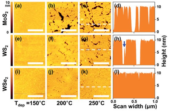
Recently, Park et al. [
32] reported a systematic study on the thermal ALD of Al
2O
3 on the surface of multilayers of TMDs (MoS
2, WS
2, and WSe
2) using different deposition temperatures (see
Figure 2). Inhomogeneous Al
2O
3 layers (with a large density of pinholes) were obtained using the conventional temperatures of 200–250 °C, whereas uniform coverage was observed when lowering T
dep to 150 °C. Furthermore, at the same deposition temperature, better uniformity of the deposited Al
2O
3 (~10 nm) films was observed on WSe
2 and on WS
2 than on MoS
2. This was ascribed to the larger polarizability of the W-and Se-based TMDs, giving rise to a higher adsorption energy of the TMA precursor due to electrostatic interaction.
Figure 2. AFM images and height line profiles of ALD Al
2O
3 films deposited on (
a–
d) MoS
2, (
e–
h) WS
2, and (
i–
l) WSe
2 multilayer samples at different temperatures (150, 200, and 250 °C). Images adapted with permission from [
32], copyright the Royal Society of Chemistry, 2017.
A two-step ALD process with early low-temperature (80 °C) deposition of an ultra-thin AlO
x layer and a following deposition at a higher temperature (180 °C) was also recently employed to obtain a homogeneous Al
2O
3 film with a <10 nm total thickness on MoS
2 [
43]. The low temperature, however, can be responsible for the degradation of the dielectric quality due to the reduced reactivity of the ALD precursor. In these conditions, the insulating films are generally characterized by a lower density and, consequently, by a lower dielectric constant [
58].
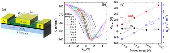
2.2. Electrical Behavior and Interface Quality of High-κ Dielectrics by ALD on 2D Materials
The quality of grown high-κ dielectrics and of their interface with the 2D material strongly influences the electrical performances of the final devices. The seed layer deposition, typically carried out ex situ, can introduce impurities and particles, which act as charge traps compromising the reliability of the high-κ dielectrics subsequently grown by ALD. Fallahazad et al. explained that the HfO
2 deposited on graphene by the evaporated Al seed layer presents a relatively low permittivity (ε = 5.5) and a low-quality interface, which is characterized by impurities and defects responsible for mobility degradation [
37,
59]. Alternatively, a method based on the in situ deposition of a metal oxide H
2O-assisted seed layer has been proposed [
41,
42]. This approach involves the physical adsorption (by Van Der Walls interactions) of a continuous layer of H
2O molecules, which acts as a site of nucleation for a seed layer of high-κ dielectrics at a low temperature (100 °C), followed by conventional deposition at 200–250°C. Fisichella et al. [
42] demonstrated that this approach ensures the optimal electrical features of the deposited dielectric on graphene, with a favorable permittivity (ε = 7.45) and breakdown field (E
BD = 7.4 MV/cm). On the other hand, significant charge trapping at the Al
2O
3/graphene interface has been observed during the operation of top-gated field effect transistors (
Figure 3a). In particular, the density of negative trapped charges up to ~4 × 10
12 cm
−2 was evaluated by capacitance voltage (C-V
TG) measurements when increasing the forward and backward gate bias sweeps (
Figure 3b,c).
Figure 3. (
a) Schematic of a top-gated graphene transistor with an ALD Al
2O
3 gate dielectric. (
b) Capacitance voltage (C-V
TG) measurements performed by sweeping V
TG from negative to positive values and back using a progressively increasing sweep range. (
c) Dirac point position (left axis) as a function of the bias sweep range for the forward and backward sweep and the evaluated density N
ot of the trapped negative charges by near-interface oxide traps (right axis). Images adapted with permission from [
42], copyright American Chemical Society, 2017.
Additionally, high-κ layers grown on 2D materials pre-functionalized by reactive gas species are subjected to charge trapping phenomena both at the interface and inside the dielectrics. As an example, the HfO
2 top gate dielectric grown on a MoS
2 surface after UV-O
3 treatment [
60] shows significant charge trapping, which can be ascribed to impurities and defects generated during the reactive gas exposure. Additionally, O
2-plasma pretreatments have been shown to have an effect on the interfacial properties and, consequently, the performance of the dielectric [
51,
52]. As an example, Zhou et al. [
61] demonstrated that remote O
2-plasma is effective for the ALD growth of Al
2O
3 on graphene, but on the other hand, they found the formation of a defective interfacial layer, resulting in a low breakdown field for the oxide (1.2 MV/cm). As previously discussed, the temperature used during the ALD process plays an important role in the uniformity of the dielectric coverage. In particular, as demonstrated in [
32,
53,
54], growth temperatures lower than 150 °C allow for achieving better uniformity, but at the same time, they result in a significant increase of trapping phenomena and, consequently, a degradation of the passivation degree [
60,
62].
This entry is adapted from the peer-reviewed paper 10.3390/app112211052