3. SPR-Optical Fiber-Based Biosensors
Localized surface plasmon resonance (LSPR) and propagating surface plasmon polaritons (SPPs) are two categories of SPR [
64]. When the size of a metallic nanostructure is smaller than the incident wavelength of light, LSPR occurs, resulting in collective but non-propagating oscillations of the surface electrons in the metallic nanostructure [
65]. The LSPR is considerably affected by the RI of the surrounding medium, making colorimetric plasmonic sensors possible [
66,
67]. The incident EM field is also concentrated around the nanostructure by LSPR. Plasmon-enhanced fluorescence (PEF) [
68,
69], surface-enhanced Raman scattering (SERS) [
70,
71], and surface-enhanced infrared absorption spectroscopy (SEIAS) [
72,
73] are all examples of how the local EM field can affect optical effects like fluorescence, Raman scattering, and infrared absorption. The LSPR-related EM field stretches into the ambient medium (usually 30 nm) and deteriorates exponentially for a dipole.
SPPs, in distinction to LSPR, are charge oscillations circulating on the surface of thin metal films. SPP cannot be excited by free-space radiations; as an alternative, resonance excitation requires momentum matching, for instance, by periodicity in a nanostructure. The RI of the ambient medium modulates SPP, which then transduces the sensor’s signal. In PEF and SERS, SPP can also be used to modulate radiation. The evanescent EM field of SPP decomposes with a longer length (usually 200 nm) than that of LSPR, permitting the SPP to be modulated by modification at a distance greater than that of LSPR. For label-free biomolecule identification, SPP modes were utilized in sensing applications. Since SPP propagated hundreds of μm along the surface, it varied from LSPR for sensing. This had a unique benefit in that the incident laser could prevent physical contact with the sample under observation. This prevented interference from heavy background noise as well as disruption to the sample from the high-energy laser [
74].
SPR-based optical fibers operate on the theory of the guided EM wave [
75]. The biggest portion of the EM-wave propagates through the core of the optical fiber, but a minor fraction of it extends from the cladding as an evanescent field, which collides with the plasmonic metal surface, and excites the free electrons [
76]. When the frequency of the incident photon and the free electrons are complemented, the electrons begin to vibrate, and an SP wave is formed at the metal-dielectric boundary. At the resonance state, a sharp loss peak occurs, which is highly responsive to the RI of the ambient medium. SPR sensors based on optical fibers were first commercialized utilizing silica optical fibers (SOFs), then polymer optical fibers (POFs). These devices did not need expensive optical apparatus and could be used to create a dense miniaturized device with remote sensing capabilities. Temperature [
77], pressure [
78,
79], environmental monitoring [
80,
81], food safety [
80,
82], and biomedical applications [
83,
84,
85], among others, all benefited from SPR-based optical sensing in recent years. An interesting review on plasmonic fiber optic biochemical sensors was recently published in [
86], which addressed the recent developments in optical fiber-based, label-free recognition devices based on SPR effects.
For both labeled and label-free approaches, the use of optical-fiber devices as sensors provided several advantages such as size, cost, light path manipulation; nevertheless, those benefits were better reflected in label-free solutions because they offered total cost-saving and accessibility factors. Fiber-optic sensors, either as a hand-held probe or as a set of distantly controlled devices along a fiber-optic cable, might be placed into the media to be sensed, such as environmental monitoring applications [
87]. In applications like pharmaceutical science, where many experiments must be conducted simultaneously, fiber-based diagnostics were not viable with bulk optic laboratory equipment like microplate array systems. Nevertheless, there appeared to be some promising applications where the fiber sensors’ low cost and accessibility might guide to general adoption, for instance, testing for viral or bacterial diseases [
88], testing for toxins in food handling plants, and examining the water quality in urban water supply structures or the atmosphere containing toxicogenic activities, and resource mining processes.
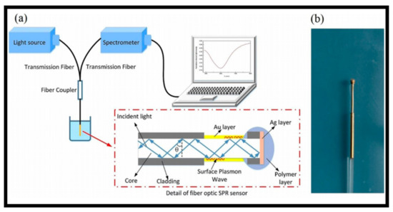
Various plasmonic sensors based on fiber-optics have lately been depicted based on the transmission probe, where noble metals were mounted on the etched cladding section, for instance, single-mode fibers (SMFs) [
89], multi-mode fibers (MMFs) [
90], wagon wheel fibers [
91], U-shaped fibers [
92,
93], D-shaped fibers [
94], and Bragg grating fibers [
95], among others [
96,
97]. Biochemical reactions usually result in small RI changes in the ambient medium, and SPR-optic fiber devices are extremely vulnerable to these minor RI variations. As a result, these sensors became common in a variety of biosensing applications. An SPR-based optical fiber biomedical sensor for the recognition of CRP in serum was proposed [
98,
99]. a illustrates a schematic of an SPR-optic fiber-based biosensors. When incident light passed through the fiber core with an incident angle larger than the critical angle, the evanescent field produced by the absolute reflection of the incident light revealed through the metal film at the same time. Strong light absorption happened as the parallel part of the incident light wave vector matched that of the SP wave. As a consequence, the output signal showed an SPR dip at a certain wavelength, defined as the resonance wavelength. The photo of the fabricated SPR sensor is shown in b. An SPR-optic fiber DNA biosensor was proposed in 2013 for the selection of DNA aptamers against the main peanut allergen protein, Ara h 1, which provided an alienation constant of 353 ± 82 nM [
100]. In 2015, researchers demonstrated an extremely sensitive, label-free, and selective SPR-optic fiber-based glucose measuring device. It had a sensitivity of 1.514 nm (mg/mL)
−1 and could detect concentrations ranging from 0.1 to 2.5 mg/mL [
101]. An SPR-optic fiber-based biochemical sensor for evaluating infliximab concentrations in the serum of inflammatory bowel illness patients was recently demonstrated, which provided a DL of 0.3 ng/mL [
102].
Figure 8. Surface plasmon resonance (SPR)-based fiber optic sensing technique: (
a) graphic illustration of the experimental arrangement. Reprinted from ref. [
99]; (
b) picture of the manufactured fiber optic SPR sensor. Reprinted from ref. [
99].
In 1978, the photonic crystal fiber (PCF) concept was proposed for the first time. It was proposed that a fiber core be clad with Bragg grating, which is like one-dimension (1D) [
103]. The first PCF was reported in 1996 at the Optical Fiber Conference (OFC) [
104], and it was composed of a 2D-PC with an air core. PCFs have a core and cladding that are identical to traditional optical fibers, but PCFs have a periodic air-hole in the cladding region that controls light propagation. Changing the geometry of air holes and the number of rings can be used to control the light propagation [
105]. In [
106], the first fiber-based plasmonic phenomenon was demonstrated by substituting graphene for the metal film and using thermal chemical vapor deposition (CVD) to produce a thin layer of graphene. An improvement in the sensing capability of SPR sensors with a graphene layer on top of Au/Ag was also demonstratable as compared to corresponding SPR sensors without the graphene layer [
107,
108,
109]. The use of Au as an active plasmonic medium, as well as the selective penetration of the PCF core with a high RI to achieve the reconciliation of positive and negative index effects, was investigated [
110]. D-shaped PCF sparked a lot of interest in SPR sensing due to its ease of production and utilization. The top surface of the fiber cladding was tailored to make it smooth, like how the metal layer and sample were mounted on top of the flat fragment in a D-shape. The metal layer in D-shape PCF could be placed close to the core, promoting close contact with the sample and improving system efficiency. Many D-shaped PCF sensors were developed to date for a variety of applications [
111,
112,
113,
114,
115].
Sensing with PCF SPR is a promising and successful technology. These sensors, on the other hand, are still in the early stages of device production technology. Mainly, the findings in the studies used a proof-of-concept approach, as well as theoretical and computational models. Due to fabrication challenges, the usage of proven theoretical models for sensor application was inadequate. Even though a few experimental procedures were published in the literature, their implementations are limited [
116,
117]. As a result, the empirical performances of the modeled sensors remain unexplored. Future research must concentrate on proving proof-of-concept for real PCF SPR sensor processing and analyte recognition for a wide variety of chemical and biological samples. One future advancement path for the PCF SPR sensors was transportable and instant lab-on-chip analyses for point-of-care diagnostics. The aim should be to switch existing fluorescence detecting with label-free PCF SPR detecting, enhancing the capability to detect a variety of analytes, reduce test expenditures, and conserve time by lowering sample formulation time. Unlike fluorescent sensors, the PCF SPR could be engineered to be redundant for purposes that need constant monitoring. As a result, PCF SPR device configurations should be made straightforwardly and cost-effectively.
A brief explanation concerning the metals employed in fiber SPR and LSPR technologies was discussed. Using well-recognized technologies like electroless deposition [
118], electroplating [
118], or sputtering [
119], thin noble metal layers could be effectively placed on optical fibers. The last of these is most frequently used, and it delivers exceptionally high-quality metal thin films. A 5 nm to 10 nm chromium or titanium buffer layer is frequently inserted between the optical fiber surface and gold layer to enable adhesion. An alternative is to thermally anneal the gold coating, which adjusts its morphology and increases its durability [
120]. It is crucial to remember that obtaining exceptionally uniform metal layers at the thickness needed for optimal SPR excitation (~50 nm) is difficult, and consequently, rugosity or fragments can form instead of smooth layers. Since the effective complex permittivity of the metal layers differed from that of the bulk values, this impacted the SPR properties (which were often used in the design of the sensors) [
121]. The utilization of non-metal layers for plasmonic applications, for example, some forms of semiconductors and oxides, has been significant; current progress on the materials side, as discussed recently [
122], still has to be investigated in fiber-based structures, although they exemplified promising research directions. An interesting review of alternative plasmonic materials beyond gold and silver was presented in [
123].
Microstructured optical fibers (MOFs) are described by a sequence of air holes that run along the length of the fiber [
124,
125,
126]. The geometry, size, and relative location of the air holes define the optical properties of this type of fiber. MOFs with high evanescent fields in the air holes can be built and manufactured by varying these parameters. The use of MOF in biochip applications was demonstrated for the first time in 2006 [
127]. An optic-fluidic coupler chip made of PMMA polymer and fabricated with a CO
2 laser contained a 16 mm long fragment of MOF. The developed chip configuration allowed continuous liquid flow control and instantaneous optical characterization via the MOF. The MOF was functionalized to catch a particular single-stranded DNA string when inserted into the chip by immobilizing a sensing layer on the microstructured internal surfaces of the fiber. The sensing layer comprised a DNA string that was paired to the target DNA string, permitting extremely selective DNA hybridization. The evanescent wave sensing theory was used to detect the captured DNA optically. The presented method permitted the analysis of sample volumes as small as 300 nL and the production of miniaturized transportable devices due to the tiny chip size [
127].
4. Metal-Insulator-Metal WG-Based Biosensors
Over the past few years, metal-insulator-metal (MIM) WG configuration has been widely studied due to its appropriateness for conducting SPP waves. SPPs are optical waves that travel along with a dielectric-metal boundary, making them interesting for several purposes [
128,
129,
130]. SPPs are strictly constrained to dielectric-metal interfaces penetrating ~10 nm into metal (identified as skin depth) and usually more than 100 nm into dielectrics (depending on the wavelength). These WG structures can be combined with different shapes of air cavities to create a compact and dense RR configuration, which can be used in several applications [
131,
132,
133,
134], out of which biochemical sensing, for example, the solution concentration and pH value, which can be evaluated through RI variations is the most widely studied topic. Compared to the other optical sensors, these structures have superior parameters of sensitivity and precision as well as much smaller dimensions. Several attempts were made to improve the size and shape of the resonator cavity, which could lead to better sensitivity and transmission, which in turn determined the quality factor (Q-factor) and figure of merit (FOM) of the sensor.
Recently, we presented several RI plasmonic sensor designs based on SPP waves to effectively use them in biomedical applications [
17,
37,
135,
136,
137,
138,
139,
140,
141,
142]. There were several other biomedical applications, such as photothermal therapy [
143,
144], blood group detection [
145,
146], glucose sensing [
147,
148], cancer cells [
147], bacillus bacteria [
147] that were also studied based on MIM WG configuration. a–f shows unique sensor designs proposed by different researchers for RI sensing applications [
17,
140,
149,
150,
151,
152]. These sensors exhibit outstanding sensing performance, which incorporates high sensitivity (S), high-quality factor (Q-factor), and noteworthy figures of merit (FOM). The sensitivity (S) can be expressed as S = ∆λ/∆n, where ∆λ is the change in λ
res, and ∆n is the variance of the ambient RI. A noteworthy factor in a wavelength filter is the ability to have elevated wavelength selectivity, which signifies a high-quality factor (Q-factor). The Q-factor can be donated as Q = λ
res/FWHM, where FWHM is the full width at half-maximum of the transmittance spectrum. Likewise, FOM is determined as S/FWHM. A compact plasmonic coupled device based on a MIM WG has a single resonance cavity, as well as a clear and broadband tunable spectrum for sensing applications. As a result, optimizing the sensor configuration for the best performance is a critical problem in designing a plasmonic MIM WG RI sensor [
153,
154].
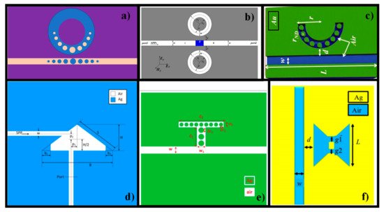
Figure 9. Recently proposed metal-insulator-metal (MIM) WG plasmonic sensors for biochemical applications: (
a) RR coupled to a MIM WG containing tapered defects. Adapted from ref. [
150]; (
b) tunable plasmonic band-pass filter with dual side-coupled circular RRs. Reprinted from ref. [
149]; (
c) nanodots arranged MIM semi-RR cavity for biochemical sensing applications. Reprinted with permission from ref. [
17]; (
d) multiple Fano-like MIM plasmonic arrangement established on triangular resonator for refractive index (RI) sensing. Reprinted from ref. [
151]; (
e) MIM WG-coupled T-shape cavity with metal nanorod defects. Reprinted from ref. [
152]; (
f) plasmonic Bow-Tie configuration. Reprinted from ref. [
140].
The expansion of analytical and numerical simulation software, for instance, COMSOL and Lumerical, which are commercially available, offered a better chance of understanding the optical characteristics of plasmonic sensor structures. Several systems, such as E-beam and ion beam lithography, could be used to fabricate nanostructures for plasmonic sensors, allowing for the lucrative fabrication of plasmonic devices over sizable regions. Furthermore, wet chemical etching or vapor deposition methods might be used to simply manufacture metal nanoparticles. Nevertheless, the objective of this paper was not to go over these processes in-depth. As a substitute, we recommended a few review papers providing detailed knowledge on this important topic [
155,
156]. Two recent reports on the development of plasmonic sensors established on MIM WGs were provided [
157,
158] for the readers interested in obtaining detailed knowledge on their working mechanism, suitable materials, fabrication process, and applications.
5. Metasurfaces for Biosensing
Veselago anticipated the development of synthetic materials by manipulating their permittivity and permeability in 1968 [
159]. This was finally discovered by the works of Pendry et al. [
160] and Smith et al. [
161], which made Veselago’s hypothesis come true and revolutionized our perception of electromagnetics. These so-called metamaterials are artificial composite nanostructures with special characteristics for manipulating light and display a variety of stimulating novel optical effects and functions that natural materials cannot accomplish [
162,
163,
164,
165]. Metasurfaces (MSs) are structures that take advantage of the miniature footprint of metamaterials. They are fairly straightforward to produce and have a reduced size than traditional optical elements. They are made up of optical elements decorated on a surface with subwavelength sizes that form the wavefront of light to present an anticipated optical phase spatial profile which has directed to the invention of ultrathin optical elements with different capabilities that outperform their bulkier rivals [
165,
166]. Additionally, this new optical phenomenon demonstrates the EM spectrum spanning from visible to terahertz (THz) frequencies [
167]. These MS-based flat systems constitute a new type of miniature, flat, and lightweight optical elements. Intensive research was conducted to employ MSs for biomedical applications [
168,
169,
170].
All-dielectric asymmetric MSs, which are made up of groups of meta-atoms with broken in-plane inversion symmetry, have recently been discovered to have high-quality resonances resulting from the exciting physics of bound states in the continuum [
171]. Dielectric MSs and hyperspectral imagining were merged in an intriguing approach to creating an ultrasensitive label-free analytical platform [
169]. This method could collect high-throughput digital sensing data at an extraordinary level of fewer than 3 molecules/μm
2 by using smart data-processing tools and could collect the spatially solved spectra from millions of image pixels. This unique sensor architecture allowed spectral data extraction from a single image without the use of spectrometers, concreting the path for compact analytical applications. The potentials of dielectric MSs to analyze biological entities and atomic-layer thick 2D structures over wide areas were extended thanks to a fruitful amalgamation of nanophotonics and imaging optics. Spectral data recovery from a single image, devoid of applying spectrometers, supported by this exceptional sensor layout was demonstrated, paving the way for transportable diagnostic applications. Dielectric MSs could now analyze biological units and atom-layer thick 2D materials over wide areas thanks to a fusion of nanophotonics and imaging optics. A new category of RI sensor established on all-dielectric gradient MS was proposed and analyzed. A unique approach of optical data processing, which was established on intensity distribution over several diffraction orders, was proposed. The intensity of 4450%/RIU and the phase sensitivity of 1200
o/RIU were demonstrated [
172]. The sensor design based on gradient MS is demonstrated in a,b [
172].
Figure 10. (a) The design of sensor-based on gradient metasurface (MS). Reprinted with permission from ref. [
172]; (
b) possible optical sensing scheme. Reprinted with permission from ref. [
172].
Endoscopic optical imaging with high resolution is a well-known technique in biological imaging for analyzing inner organs. Optical coherence tomography (OCT) is an imaging procedure that can acquire tissue microstructures at millimeter depths in the tissues and has been employed for clinical diagnosis in head and neck cancer, cardiovascular disorders, and dermatology. OCT detects changes in the sample’s RI using a low-coherence light interferometry setup and, thus, provides morphological details. A medical endoscopic optical imaging system established on OCT with a metalens was developed [
173]. It discussed the problems of spherical and chromatic aberration, all of which were unacceptable. There were some other notable works on MSs based flat optics [
174,
175,
176] and endoscopic optical imaging [
177,
178]. MS biosensors were also used to identify cancer biomarkers, such as breast, liver, and oral cancer. For the recognition of breast cancer biomarkers, an optofluidic MS biosensor was created [
179]. Another example was the assessment of biomarkers for liver cancer [
180]. The apoptosis of oral cancer cells was analyzed using an electromagnetically induced transparency (EIT) like MS [
181].
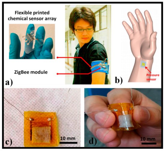
Wearable sensor technology is a critical connection to personalized medicine in the future. It is important to acquire a full picture of human health; however, tracking several analytes within the body at the same time is difficult. The researchers depicted a wearable plasmonic-electronic sensor with universal molecular identification capability [
182]. Since the practical task of preserving the plasmonic activities of the fragile nanostructures under different distortions was resolved, a compliant plasmonic MS with SERS-activity was established as the basic sensing module in a wearable device. The proposed sensor, when used in conjunction with a versatile electronic sweat removal system, could noninvasively extract and fingerprint analytes within the body established on their spectral SERS spectra. The variety of trace-amount drugs within the body was effectively tracked, and an individual’s drug metabolic profile was obtained as a proof-of-concept illustration. By offering a universal, responsive molecular examining means to evaluate human health, the sensor filled a void in wearable sensing technology [
182]. An attractive design of a wearable electronic nose for armpit odor testing was suggested in [
183] by utilizing an economical chemical sensor array incorporated in a ZigBee wireless communication network. a describes the model of the fabricated wearable e-nose. The mask kept the sensor surface from rubbing but permitted the free passage of the air and odors. The body odor could be easily gathered from the armpit area using this sensor. The sensor resistance as a function of the displayed VOCs and their concentrations were used to verify the odor data. The system used ZigBee technology to transmit data from the sensor to the computer, which is well known as a low-cost wireless network communication [
183]. In [
184], a wearable and adaptable pressure sensor design was proposed, which was critical for the continuous monitoring of a person’s health. It showed an excellent performance with the accord of numerous qualities, containing high sensitivity for a broad pressure range and an ultralow energy intake level of 10
−6 W. Furthermore, pressure sensors might be incorporated onto robots as artificial skins, allowing them to feel pressure and the dispersal of pressure through the synthetic skin. The sensor was attached to the artery vessel at the wrist, as shown in b, to reveal their potential of detecting human vital physiological signals [
184]. The optical images of the assembled unit are revealed in c,d, and the pressure provided excellent versatility. After being decorated with single-walled nanotubes, the sheet resistance of paper sheets decreased to about12.6 kΩ, which was adequately conductive to be used as an active layer in a pressure sensor [
184].
Figure 11. (a) Model of a wearable e-nose established on the adaptable inkjet-printed chemical sensor array incorporated in ZigBee wireless network. Reprinted from ref. [
183]; (
b) pressure sensor was attached to a human wrist for heart pulse detection. Reprinted from ref. [
184]; (
c) photograph of a manufactured pressure sensing device connected with Al wires. Reprinted from ref. [
184]; (
d) photograph of a bent pressure sensing device. Reprinted from ref. [
184].
6. Photonic Crystals-Based Biosensors
Biomarkers have been detected using sensitive biosensing technologies such as SPR, electrochemical biosensors, and, more newly, inverse opal photonic crystal (PhCs) biosensors [
185,
186,
187]. The invention of PhCs in 1987 by Yablonovitch [
188] and John [
189] sparked a lot of interest. EM waves propagated inside the PhC, and disruptive interference occurred for certain wavelengths, resulting in a photonic bandgap (PBG), which was close to the energy bandgap of electron waves in a semiconductor. It might be possible to control light propagation due to the likelihood of producing PBG. Light bending [
190,
191,
192], optical diode [
193], negative refraction [
194], and self-collimation [
195] were only a few of the notable applications of PhCs. Currently, PhCs biosensors were employed to identify a wide range of biological analytes selectively and sensitively, including DNA, cells, bacteria, proteins, and antibodies. This allowed for improved sensing efficiency concerning limit-of-detection (LOD) [
196].
Various studies in PhC bioassays and their usage in bio-systems have been published to date, with an emphasis on the physical and optical activity of PhCs [
197,
198]. In [
199], a detailed description and understandings of the inverse opal bio-sensing procedures for detecting biological factors such as viruses, proteins, and DNA were presented. Photonic Bragg diffraction planes could be formed in inverse opal structures with periodic arrays because of high and low dielectric zones. The photonic band’s optical properties contributed to their use in bio-sensing systems. By binding biomarkers to pore surfaces or flowing liquids through inverse opal pores, the detection process in inverse opal configurations was associated with a shift in RI in the pores and voids of inverse opal films. These variations preceded the blue/red shift in PBG in reflected wavelength spectra and color modifications in inverse opal thin-films [
200]. The porous structure of the inverse opal created a large surface area for small molecule recognition. The optical properties of the exceedingly ordered inverse opal were supposed to be fine. Optical investigations revealed that different pore sizes in inverse opal resulted in different reflection or transmission spectra [
201,
202].
Due to their potency in portable point-of-care-testing tools and color metrics for graphical biosensor applications, inverse opal label-free materials are appealing and appropriate sensing systems for the recognition of proteins. Inverse opals may be used to diagnose biological particles without the use of advanced research tools because of their intuitive structural color [
203]. The detection of alpha-fetoprotein (AFP), a liver cancer biomarker, was proposed using a photoelectrochemical biosensor founded on ZnO inverse opal with a LOD of 0.01 ng/mL. ZnO inverse opal and quantum dots were used on the photoelectrochemical electrode surface in this analysis [
204]. In another study, an inverse opal biosensor based on inverse opal-Ag
2S NPs was proposed for the detection of AFP [
205]. The ZnO inverse opal/Ag
2S composite resulted in the production of long-wavelength light absorption. The LOD for AFP detection was 8 pg/mL, which was nearly 1.5 times higher than the former process. This outcome was due to better photo-generated electron conduction in ZnO inverse opal/Ag
2S structures due to the successful matching of energy levels among the transmission bands of Ag
2S and ZnO inverse opal [
205]. Apart from the TiO
2 based inverse opal, IOH nonporous arrangements could be employed in label-free and selective recognition of the IgG antibodies [
206]. With increasing IgG concentration, the color of the IOH structure shifted from green to orange, which could be seen with the naked eye, as well as a 50 nm bandgap shift in absorbance spectra.
Utilizing self-assembled Au nanoparticles conjugated with biotinylated anti-gp120 polyclonal antibodies to particularly capture and identify HIV, a nanoplasmonic-based platform was designed [
207]. Via impedance spectroscopy of viral lysate samples, an electrical sensing process was established to identify captured HIV-1 on magnetic beads coupled with anti-gp120 antibodies [
208]. PhC biosensors, for example, use dielectric permittivity variations at the interface of a transducer substrate and a liquid media to provide a fast and precise optical recognition procedure for biomolecules, cells, and viruses [
209]. In this case, optical detection using PhC biosensors for instantaneous monitoring of virus infection can be more valuable than laborious pathogen-specific molecular recognition methods such as polymerase chain reaction (PCR) and enzyme-linked immunosorbent assay (ELISA). The unharmed virus particles in actual test samples were detected using instant and responsive viral PhC sensing procedures that did not involve labeling or multiple chemical alteration methods. By immobilizing antibodies on the periodic arrangements of the PhC surface, a reflectometric 2D PhC biosensor was developed for the recognition of the influenza virus in human saliva with a LOD of 1 ng/mL [
210].
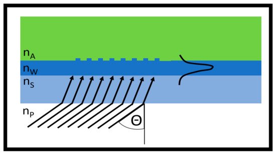
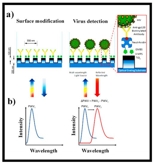
Early discovery of the virus applying non-invasive, high-sensitivity, and innovative bio-sensing methods was highly successful in keeping the individual safe from viral infections [
211]. As shown in a, the periodic composition of dielectric material on a PhC sensor caused the formation of an optical resonance at a specific wavelength, at which EM standing waves spread into the liquid media in contact with the PhC surface. The PhC nanostructures were created by replica molding of a low index polymer, which was then covered with a high index TiO
2 dielectric layer to form a periodic surface structure. When lit up with a paralleled broadband light at a normal incidence angle, the PhC configuration reflected only a small resonant band of light with practically 100% efficacy, whereas all other wavelengths were transmitted. When biological samples like proteins, viruses, or cells connected to the PhC, the peak wavelength value (PWV) of the reflected resonant continuum moved to a greater value, as shown in b.
Figure 12. Schematic of PhC-based virus recognition platform. (
a) The bottom surface of PhC biosensor microplate wells is made up of a nanostructured subwavelength grating that is covered with TiO
2. Reprinted from ref. [
211]; (
b) binding occurrences inside the immediate proximity of the sensing area alter the bulk RI; therefore, the peak wavelength value (PWV) of the reflected light is changed. The swing in the peak wavelength (DPWV) is in direct proportion to the attachment of molecules and/or bioagents onto the biosensing surface Reprinted from ref. [
211].
7. Photonic Biosensing with Thin Metal Films
Sample handling, biological detection and amplification, transduction, and electronic signal processing are all areas where thin films are used in biosensor systems [
212,
213]. Several planar microelectrochemical chips on Si or glass substrates with thin-film electrodes of various shapes and arrangements have been developed and utilized in voltammetric and potentiometric sensors. Bilayer lipid membranes (BLMs) are thin-film materials that are flexible and can be used in biosensors [
214,
215]. The use of thin-film electrodes to develop BLMs on a planar chip revealed new possibilities to produce miniaturized biosensors along with basic research into the electrical and mechanical properties of biological membranes. It was 30 years ago that the first effort to build BLMs was made [
216]. However, the solvent was held in the structure of the membranes, and the results cannot be replicated. Methods for making solvent-free lipid membranes were also presented, but their main downside was that these films were extremely brittle and susceptible to collapse when subjected to mechanical or electrical shock [
217]. The literature documented methods to enhance the constancy of these lipid films, such as interconnected membrane bubbles in organic solvents without a substrate aperture or the so-called monolayer technique [
218].
Biosensors of the current generation are analytical lightweight instruments made of thin films. The main benefits of these biosensors are their sensitivity, accuracy, rapid response time, accessibility, and small cost. All these characteristics are closely linked to the thickness of the films used in the sensor fabrication [
219]. The interaction of the biological analyte with the surface-modified thin film is the key basis for a biosensor’s detection principle. The thin film functions as a physiochemical-optical, mechanical, magnetic, and electrical transducer, converting the signal produced by the biological analyte recognition into another observable signal [
220]. SPR spectroscopy is a well-known analytical method for quantifying molecular interactions at an interface without using labels. The technique works by identifying slight variations in RI of a dielectric medium in contact with a thin metal film on the nanometer scale. Gold (Au) has historically been used as the metal layer because of its elevated plasmonic activity and chemical inertness. Further, metals such as chromium (Cr), copper (Cu), and aluminum (Al), on the other hand, are receiving more attention as plasmonic materials. Al has a higher electron density and a higher negative permittivity than Ag or Au, making it remarkably interesting [
221]. Al is plasmonically active from the UV to the near IR regions due to this attribute, which causes plasmonic resonance over a broad wavelength range [
222]. Al is also attractive for industrial applications because of its abundant supply, low cost, and ease of incorporation into manufacturing processes like CMOS.
In [
223], SPR biosensing with Al thin-films was demonstrated employing the traditional Kretschmann structure that had formerly been overshadowed by Au films [
224]. In both bulk and surface samples, Al films displayed excellent sensitivity efficiency in both classifications. In comparison to Au, the Al/Al
2O
3 layer had a significant effect on controlling nonspecific binding in blood serum. When used for SPR imaging research, Al film had a higher sensitivity and a broader working range than Au films, according to further characterization. The Al thin-film, when combined with its cost and processing advantages, can become an extremely beneficial plasmonic substrate for a large range of biosensing functions in SPR formations. In [
225], the cholesterol sensors comprising of a blend of cholesterol oxidase (ChOx) and zinc oxide (ZnO) nanoparticles were cultivated on ITO/glass substrates by thermal evaporation technique, and their sensing attributes are analyzed in air.
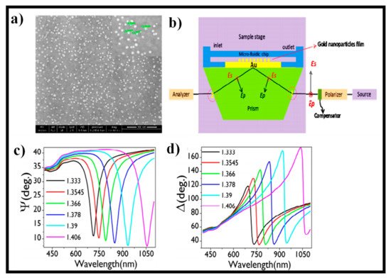
In [
226], an ellipsometry study on gold nanoparticles (AuNPs) coated on Au thin film was demonstrated for biosensing applications. The SPR dip could be tuned from the visible to near-IR merely altering the AuNP concentration. a reveals the SEM photograph of the distribution of the AuNPs on the gold surface after a 1-min treatment of the amine-functionalized gold substrate. These samples were placed on the dove prism using a microfluidic flow cell to comprehend the optical properties of different AuNPs’ distribution immobilized on the Au substrate in water. b depicts the architecture of the experimental setup in the TIR arrangement. With this system, the optical response of various samples was measured using ellipsometry signals (Ψ, Δ). Bulk sensitivity tests were performed to calibrate the SPR unit based on ellipsometric signals (Ψ and Δ) and by infusing glycerol-water mixtures of different concentrations with different RI values onto the sensing surface via the microfluidic flow cell as indicated in c,d. A refractometer was utilized to measure the RI values of various glycerol-water mixtures.
Figure 13. (
a) Distribution of AuNPs on the Au surface after 1-min treatment of amine-functionalized Au substrate. Reprinted from ref. [
226]; (
b) graphical illustration of the experimental setup with optical components showing the polarization of the incident and reflected light within the prism for a sample attached perpendicular to the sample stage. Reprinted from ref. [
226]; (
c,
d) spectral response of the ellipsometric parameters Ψ, Δ for glycerol-water mixtures having different refractive indices introduced on 30 min treated AuNPs-coated Au substrate. Reprinted from ref. [
226].
8. Fiber Bragg Grating Biosensors
Researchers have so far investigated fiber grating sensors, some of which are now commercially available. Fiber Bragg grating (FBG), long-period grating (LPG), chirped fiber grating (CFG), tilted fiber Bragg grating (TFBG), etched fiber Bragg grating (EFBG), and sampled fiber grating (SFG) are the different kinds of fiber gratings, with FBG being the most common in sensor design [
227,
228]. FBGs may be photo imprinted onto fibers, and the resulting FBG sensors are usually strain and temperature-sensitive. High sensitivity, multiplexing capability, compact size, multi-modal sensing ability, tolerance to EM intervention, and low production cost are all advantages of optical fiber grating-based sensors. Owing to their label-free design of quantifying RI, optical grating sensors such as LPG, EFBG, and TFBG sensors are becoming more common in the development of chemo- and biosensors [
229]. Some of these FBG biosensor configurations have been tested in the hopes of improving thrombin biosensors [
230,
231]. Thrombin is involved in both normal and abnormal coagulation, and its normal concentration ranges from nanomolar to low micromolar during blood coagulation [
232]. Thrombin levels can rise when tumor cells cause blood coagulation both extra- and intravascularly. Thrombin is implicated in a variety of diseases, including atherosclerosis, thromboembolic disease, cancer, and inflammatory disease, so finding it in the blood is crucial for both study and clinical applications [
233]. Because of its clinical significance, there has been a lot of research into detecting thrombin, with the bulk of it focusing on aptamers.
An FBG sensor, on the other hand, cannot conduct RI-based sensing because the optical field is limited to the fiber core [
234]. For this purpose, the evanescent field must interact with the ambient medium, which can be accomplished by polishing [
85], etching [
235], or tapering the fiber [
236]. The wavelength response of the Bragg grating, which is determined by the bulk RI, will appear when the FBG is immersed in a sample liquid. In [
237], hydrofluoric acid (HF) was used to etch the fiber cladding at the Bragg grating points, which amplified the light-matter interaction. For RI bulk sensing, a thinned FBG sensor was presented [
238]. The experiment used glycerin solutions with well-recognized RIs to assess sensor sensitivity. A highly sensitive etched-core FBG sensor was proposed, which detected any external RI change by measuring the shift in λ
Bragg. The sensitivity value was 1394 nm/RIU when the fiber core was reduced to a diameter of 3.4 μm, and the RI of the surrounding area was like that of the fiber core [
239]. Higher-order modes yielded higher sensitivity in detection when the RI of the surrounding was less than that of the fiber core, e.g., the second-order mode yielded a sensitivity of 404 nm/RIU compared to the fundamental mode’s sensitivity of 171 nm/RIU. Finally, the FBG sensor was used to detect DNA molecule hybridization. The hybridization of target DNA molecules was observed, and a wavelength shift of 73 pm, equivalent to a RI change of 2.5 × 10
−3, was measured. The in-situ monitoring of bioprocesses was possible with this FBG sensor [
239].
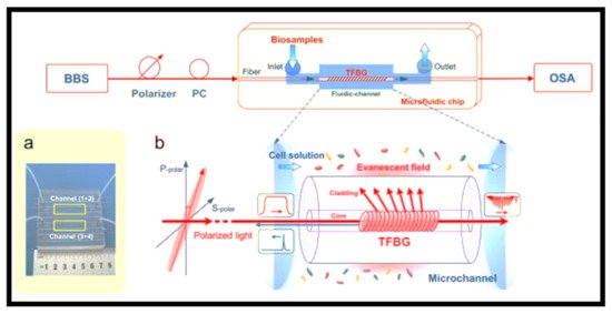
FBG biosensors can be employed as a cost-effective and comparatively simple-to-realize option to well-established biosensor platforms for superior sensitivity biological sample measurements in situ or probably in vivo [
240]. A fiber biosensor employs an in-fiber 12
° tilted Bragg grating to stimulate a robust evanescent field on the sensor’s surface over a wide range of outer medium RIs. Human acute leukemia cells with different intercellular densities and RIs ranging from 1.3342–1.3344 were unambiguously distinguished in situ by utilizing the differential transmission continuum between orthogonal polarizations. An amplitude deviation sensitivity, wavelength variation sensitivity and LOD were 1.8 × 10
4 dB/RIU, 180 nm/RIU, and LOD of 2 × 10
−5 RIU were obtained, respectively. A microfluidic chip that allows the measurement of nL-volumes of biosamples was used to precisely monitor the detection process, as shown in a [
240]. The proposed in-fiber polarimetric biosensor was an appealing solution for rapid, sub-μL dose highly sensitive detection of analytes at low concentrations in medicine, chemical, and environmental monitoring. b shows a graphical representation of a TFBG biosensor probed with tunable linearly polarized light [
240].
Figure 14. Polarimetric tilted fiber Bragg grating (TFBG) sensing system: (
a) micro-fluidic chip for biosample measurements. Reprinted with permission from ref. [
240]; (
b) schematic diagram of polarimetric TFBG biosensor interrogated with tunable linearly polarized light. Reprinted with permission from ref. [
240].