The field of flexible electronics is undergoing an exponential evolution due to the demand of the industry for wearable devices, wireless communication devices and networks, healthcare sensing devices and the technology around the Internet of Things (IoT) framework. E-textiles are attracting attention within the healthcare areas, amongst others, for providing the possibility of developing continuous patient monitoring solutions and customized devices to accommodate each patient’s specific needs.
- textile materials
- flexible resonator
- textile resonator
- wearable device
- washing analysis
- bending analysis
- embroidered resonator
1. Principle of Operation and Classification of Microwave Resonators
1.1. Principle of Operation of Microwave Resonators
1.1.1. Resonance Frequency and Quality Factor: A Brief Description


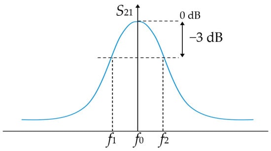


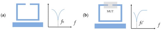
1.1.2. Frequency Variation as a Sensing Principle
1.2. Classification and Configurations of Resonators
1.2.1. Types of Resonators
- ○
-
Lumped-element resonator and quasilumped-element resonator, which resonate accordingly to the aforementioned Equation (1).
- ○
-
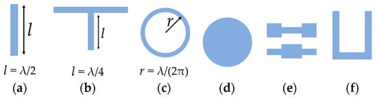
Distributed line resonators, which resonate at a frequency, f, that is a function of the fundamental resonance frequency, f0.
-
Quarter-wavelength (λ/4) resonator (f ≈ (2n − 1) f0 for n = 2, 3, …) with shunt series or shunt parallel resonance.
-
Half-wavelength (λ/2) resonator (f ≈ nf0 for n = 2, 3, …).
-
Ring resonator, whose resonance frequency is a function of the ring radius, r (2πr = λ, f ≈ nf0 for n = 2, 3, …).
-
And others: stepped impedance resonator (SIR), hairpin resonator, etc.
-
- ○
-
Patch resonators, which can be shaped into numerous geometries such as circular or triangular.
-
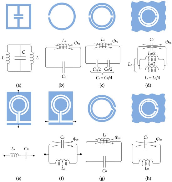
Electric-LC (ELC);
-
Ring resonators:
- ○
-
Split-ring resonator (SRR);
- ○
-
Complementary split-ring resonator (CSRR);
- ○
-
Open split-ring resonator (OSRR);
- ○
-
Open complementary split-ring resonator (OCSRR);
- ○
-
Spiral resonator (SR);
- ○
-
Complementary spiral resonator (CSR).
2. Materials and Methods in Flexible Electronics
-
Optical properties: low birefringence and clear substrates are a must for displays.
-
Surface roughness: asperities impact on the electrical function.
-
Thermal and thermomechanical properties: the substrate’s working temperature must support the maximum fabrication process temperature.
-
Chemical properties: avoid contaminants release.
-
Mechanical properties: an elevate elastic modulus is necessary to grant the substrate’s bending and stretching.
-
Electrical and magnetic properties: substrate must either conduct or insulate as per the designs’ requirements.
| Layer | Applications | Materials |
|---|---|---|
| Substrate Materials | Polymers | PVA, PET, PI, PU, PE |
| Flexible and stretchable | PEN, PDMS | |
| Eco-friendly and biodegradable | Paper, chitin, silk, gelatin | |
| Electrode Materials | Soft metals | Galinstan alloy, metal nanoparticles and nanowires |
| Conductive nanomaterials | Carbon materials: graphene, carbon nanotube | |
| Conductive polymers | PEDOT: PSS, PANI | |
| Hybris materials | Carbon/metal, polymer/metal | |
| Functional Materials | Cluster materials | Molecules, polymers, biomass |
| Low-dimensional and nanomaterials | Nanoparticles and Quantum dots Nanowires, nanotubes and nanoribbons Graphene, transmission metal dichalcogenides and mXenes |
|
| Organic–inorganic hybrid materials | Nanomaterials/polymers |
2.1. Conventional Substrates
| Property | Metal Foil | Plastic Film | Thin Glass |
|---|---|---|---|
| Thickness, t | Stainless steel 430 100 μm |
PEN, PI 100 μm |
Glass 1737 100 μm |
| Flexibility | At t < 125 μm | High | At t < 100 μm |
| Young’s modulus, E | Stainless steel 430 200 gPa |
PEN, PI 5 gPa |
Glass 1737 70 gPa |
| Optical transmission visible | Opaque | PEN and PET semitransparent (optical transmittance >85%) | Semitransparent (optical transmittance >90%) |
| Resistance to process chemicals | High (Stainless steel) |
Poor for PC, PES, PAR, PCO | Resistance to most of them |
| Dimensional stability | High | Lower than glass | High |
| Temperature tability | High | Lower than glass | High |
| Temperature tolerance | ≤1000 °C | ≈200 °C | ≤600 °C |
| Thermal conductivity | Stainless steel 430 16 W/m°C |
PEN, PI 0.1–0.2 W/m°C |
Glass 1737 1 W/m°C |
| Electrical conductivity | Conductive Insulation requires insulating layer coating | Insulator (Except ICPs) |
Insulator |
| CTE 1 | Low (<20 ppm/°C) (Stainless steel 430, 304) | Low (<20 ppm/°C) (PET, PEN, PI) | Low (≈4 × 10⁻⁶ ppm/°C) |
| Surface roughness | ≈1 μm | ≈10 μm | ≤1 μm |
| Durability | High | Lower than metal | Lower than metal |
| Permeability against oxygen and water | Impermeable | Easily permeated by oxygen and water | Impermeable |
| Roll-to-toll processable | Yes | Likely | Not likely |
2.2. E-Textiles
2.2.1. Key Properties of Textiles in Electronics


where the Q-factor results of the reciprocal relation of losses are shown in Equation (10): space wave (Qrad) losses, conduction ohmic (Qc) losses, surface waves (Qs) losses and dielectric (Qd) losses.

2.2.2. Textile Substrates
| Ref. | Fabric | εr | tanδ | Frequency (GHz) |
|---|---|---|---|---|
| [25][26] | Felt | 1.22–1.38 | 0.0160–0.0230 | 2.45 |
| [25] | Cordura® | 1.90 | 0.0098 | 2.45 |
| [25] | Cotton 1 | 1.60 1 | 0.0400 1 | 2.45 |
| [25] | 100% Polyester | 1.90 | 0.0045 | 2.45 |
| [27] | Viscose | 1.64 | 0.0160 | 2.45 |
| [25] | Lycra | 1.68 | 0.0080 | 2.45 |
| [25] | Quartzel® Fabric | 1.95 | 0.0004 | 2.45 |
| [25] | Cordura/Lycra® | 1.50 | 0.0093 | 2.45 |
| [25] | Tween | 1.69 | 0.0084 | 2.45 |
| [25] | Panama | 2.12 | 0.0500 | 2.45 |
| [25][27] | Jeans | 1.62–1.70 | 0.0180–0.0250 | 2.45 |
| [25] | Moleskin | 1.45 | 0.0500 | 2.45 |
| [27] | Fleece | 1.20 | 0.0040 | 2.40 |
| [27] | Felt | 1.36 | 0.0160 | 2.40 |
| [27] | Silk | 1.20 | 0.0250 | 2.40 |
| [27] | Leather | 2.95 | 0.1600 | 2.40 |
| [27] | Neoprene rubber | 5.20 | 0.0250 | 2.40 |
| [27] | Cotton | 1.54 | 0.058 | 2.40 |
| [27] | Polystyrene foam | 1.02 | 0.00009 | 2.40 |
| [27] | Velcro | 1.34 | 0.0060 | 2.40 & 5.00 |
| [27] | Denim | 1.80 | 0.0700 | 2.40 & 5.00 |
| [27] | Tween | 1.69 | 0.0084 | 2.60–3.95 |
| [27] | Silk | 1.75 | 0.0120 | 2.60–3.95 |
| [26] | Polyester plain weave | 3.20–3.66 | 0.018–0.0320 | 1.00 |
| [26] | Flax | 4.22–6.20 | 0.0370–0.058 | 1.00 |
| [26] | Jute | 2.99–4.95 | 0.0310–0.0470 | 1.00 |
| [26] | Hemp | 4.08–4.77 | 0.0280–0.0520 | 1.00 |
| [26] | Wool | 4.11–5.70 | 0.0280–0.0520 | 1.00 |
| [28] | 100% Nylon 6.6 | 2.82–2.78 | 0.0268–0.0283 | 9.80 |
| [28] | Denim | 1.70 | 0.085 | 2.22–2.59 |
2.2.3. Conductive Fibers and Yarns
| Fiber Category | Material | Properties |
|---|---|---|
| Metal fibers | Stainless steel Silver Copper Aluminum Nickel Many alloys |
High conductivity (≈105 S/cm) High mechanical and thermal strength Heat and corrosion resistant Anti-static properties Electromagnetic shielding |
| Carbon fibers | Polyacrylonitrile (PAN) Pitch Viscose Carbon black Graphene |
High conductivity (≈104 S/cm) High mechanical strength Large specific surface area Low mass density Excellent mechanical properties Abrasion and wear resistance Anti-static properties are possible also |
| Conducting polymers |
Polyaniline (PANI) Polypyrrole (pPy) Polystyrene sulfonate (PEDOT: PSS) Polythiophene (PT) |
Excellent flexibility Low conductivity (the non-ionic polymers only) Poor mechanical properties Good electronic properties: high areal capacitance and areal energy density |
-
Metallic filament yarns (metallic or metallized yarns);
-
Conductive hybrid yarns;
-
Conductive composite yarns or metal composite embroidery yarns (MCEYs);
- ▪
-
Core spun yarns;
- ▪
-
Commingled yarns;
- ▪
-
Blended spun yarns;
-
Bi/multi-component spun yarns;
-
-
Inherently conductive polymer yarns (ICP);
-
Laminated/coated conductive yarns;
-
New conductive material and nanomaterial yarns.
| Yarn Category | Applications |
|---|---|
| Metallic | Fabric-based circuits Core of composite yarns Heating fabrics Antimicrobial textiles Antipiercing gloves Anti0static |
| Conductive composite (MCEYs) | Antistatic and electromagnetic shielding Antibacterial Strain sensor |
| ICP yarns | Electromagnetic shielding Simple circuit Supercapacitor |
| Plated, laminated and coated | Supercapacitor Strain sensor |
| New conductive and nanomaterial | Microelectrode Antibacterial Antimicrobial textiles |
2.3. Manufacturing Techniques
2.3.1. Etching
2.3.2. Soldering and Welding
-
Resistance welding: This requires two metallic parts to be joined by applying an electrical current through them.
-
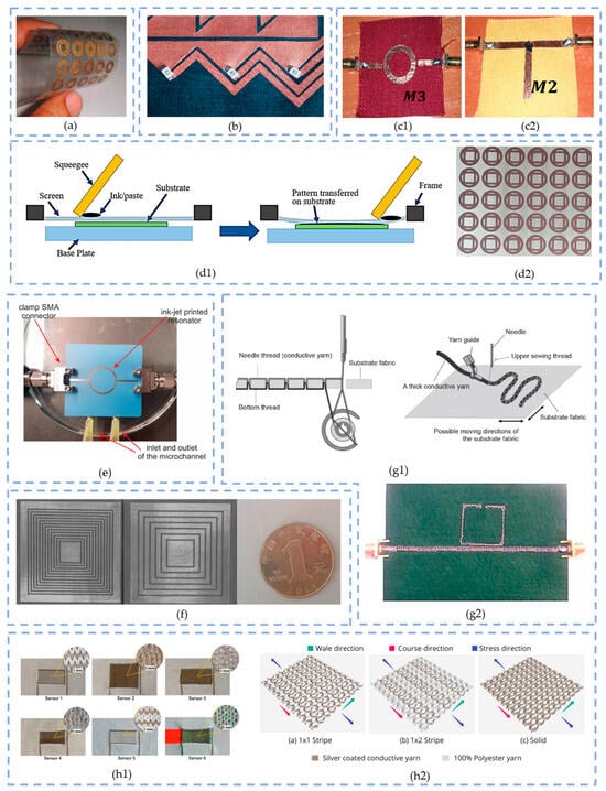
Ultrasonic welding: The ultrasonic acoustic vibrations with frequencies between 20 and 40 kHz generate heat and pressure that end up welding the two parts [42]. This is the most popular welding process with applications in multiple areas such as automotive, aerospace and health. An example is [43], where rotating ultrasonic welding technology is employed to integrate highly conductive ribbons into textile-based conductive tracks.
-
Radio-frequency (RF) welding: The RF absorbing polymer tape is positioned in the middle of the two fabric pieces, which melts by submitting to RF energy. This technique is of interest for non-weldable fabric materials.
2.3.3. Adhesive Conductive Foil
2.3.4. Printing Technologies
-
Conventional printing: These are printing technologies that require a master (printing plate), which is basically the tool that enables the ink transfer to the printing substrate. The conventional printing processes are outlined below:
-
Screen printing;
-
Letterpress/flexography;
-
Lithography/offset;
-
Gravure printing.
-
-
Non-impact printing: These are masterless printing technologies (also known as ‘non-contact printing’ processes). These technologies employ laser to transmit the information to the intermediate carrier that will afterwards transfer it to the final substrate. The non-impact printing processes are outlined below:
-
Electrophotography;
-
Inkjet printing;
-
Ionography;
-
Magnetography;
-
Thermography;
-
Photography.
-
2.3.5. Three-Dimensional (3D) Printing
-
Fused Filament Fabrication (FFF) or Fused Deposition Modeling (FDM);
-
Stereolithography (SLS);
-
Digital Light Processing (DLP);
-
Material Jetting (MJ).
2.3.6. Embroidery
2.3.7. Weaving and Knitting
-
Lightweight;
-
Portability;
-
Skin comfort;
-
Durability;
-
Deformation resistance (woven fabrics);
-
Elasticity and stretchability, air permeability, thermal retention (knitted fabrics).
2.3.8. Comparison of Wearable Electronics Integration Techniques
| Technique | Advantages | Limitations |
|---|---|---|
| Wet Etching | Controllable etching rate Complex designs High resolution |
Chemical contamination Depends on orientation Undercutting Not for small batch production Influenced by temperature and concentration of etchant High costs |
| Soldering and Welding | Low contact resistance Easy manufacture Efficient mass production Low cost Compatible with standard electronics processes Ultrasonic welding: not contaminant, biocompatible |
Mechanically fragile Requires reinforcing when bending or stretching (not flexible at all) Requires high temperature Limited materials |
| Adhesive Conductive Foil | Low cost In-house made Flexible Good for prototyping Low curing temperatures Environmentally friendly |
Disengages easily Low accuracy Not suitable for complex designs Fragile, easy to break Poor resolution High contact resistance |
| Inkjet Printing | No printed form is needed Ideal for prototyping High-quality prints Small losses |
Limited colors Elevated cost of inks Poor print quality Slow print |
| Screen Printing | Price competing Good ink processability Efficient mass production Applicable to a final product Very flexible and stretchable Ideal for simple design |
Printed form is required Long set up time Limited layer thickness Not efficient for prototyping or small batch production Huge waste of water Not possible in-house |
| 3D Printing | In-house made Fully digital Fast fabrication Flexibility in materials Complex shapes and structures Adaptable density Lightweight |
Difficult scalability High cost of AM manufactured material per weight Inconsistent quality Lossy materials Thermal instability Bending difficulties Poor resolution |
| Embroidery | 2D and 3D structures Freedom of fibers orientation Good for prototyping Reduced waste Stable textile structures Very flexible and stretchable Precise and digitized (CAD) Variety of materials Scalability, mass production |
Low precision in complex designs Difficult to automate Requires sealing to avert electrical shorting Slow process Performance impacted when bending or washing |
| Weaving and Knitting | Highly automated Stable textile structures Robust textile structures |
Requires sealing to avert electrical shorting Fragile, easy to break Limited choice of yarns Performance impacted when bending or washing |
This entry is adapted from the peer-reviewed paper 10.3390/s23229103
References
- Hong, J.; Lancaster, M.J. Microstrip Filters for RF/Microwave Applications, 1st ed.; Wiley: Hoboken, NJ, USA, 2001.
- Pozar, D.M. Microwave Engineering, 4th ed.; John Wiley & Sons, Inc.: Hoboken, NJ, USA, 2012.
- Deng, Y.; Mengxia, Y.; Shi, Z. Design of Compact Dual-Mode Dual-Band Bandpass Filter for WLAN Communication System. Available online: https://link.springer.com/chapter/10.1007/978-3-642-21765-4_98 (accessed on 16 October 2023).
- Mason, W.P.; Sykes, R.A. The use of coaxial and balanced transmission lines in filters and wide-band transformers for high radio frequencies. Bell Syst. Tech. J. 1937, 16, 275–302.
- Baena, J.D.; Bonache, J.; Martin, F.; Sillero, R.M.; Falcone, F.; Lopetegi, T.; Laso, M.A.G.; Garcia-Garcia, J.; Gil, I.; Portillo, M.F.; et al. Equivalent-circuit models for split-ring resonators and complementary split-ring resonators coupled to planar transmission lines. IEEE Trans. Microw. Theory Tech. 2005, 53, 1451–1461.
- Crabb, R.L.; Treble, F.C. Thin Silicon Solar Cells for Large Flexible Arrays. Nature 1967, 213, 1223–1224.
- Cheng, I.-C.; Wagner, S. Overview of Flexible Electronics Technology. In Flexible Electronics; Wong, W.S., Salleo, A., Eds.; Electronic Materials: Science & Technology; Springer: Boston, MA, USA, 2009; Volume 11, pp. 1–28.
- Zhou, Z.; Zhang, H.; Liu, J.; Huang, W. Flexible electronics from intrinsically soft materials. Giant 2021, 6, 100051.
- Thin Silicon Solar Cells for Large Flexible Arrays|Nature. Available online: https://www.nature.com/articles/2131223a0 (accessed on 16 October 2023).
- Overview of Flexible Electronics Technology|SpringerLink. Available online: https://link.springer.com/chapter/10.1007/978-0-387-74363-9_1 (accessed on 16 October 2023).
- Cochrane, C.; Hertleer, C.; Schwarz-Pfeiffer, A. 2-Smart textiles in health: An overview. In Smart Textiles and Their Applications; Koncar, V., Ed.; Woodhead Publishing Series in Textiles; Woodhead Publishing: Oxford, UK, 2016; pp. 9–32.
- ISO/TR 23383:2020; Textiles and Textile Products—Smart (Intelligent) Textiles—Definitions, Categorisation, Applications and Standardization Needs. ISO: Vernier, Switzerland, 2020.
- Abolade, J.O.; Konditi, D.B.O.; Dharmadhikary, V.M. Comparative study of textile material characterization techniques for wearable antennas. Results Mater. 2021, 9, 100168.
- Rhines, F.N. Microstructure-property relationships in materials. Metall. Trans. A 1977, 8, 127–133.
- GB 9994-2008 English PDF (GB9994-2008). Available online: https://www.chinesestandard.net/PDF/English.aspx/GB9994-2008 (accessed on 16 October 2023).
- Xie, Y.; Hill, C.A.S.; Jalaludin, Z.; Curling, S.F.; Anandjiwala, R.D.; Norton, A.J.; Newman, G. The dynamic water vapour sorption behaviour of natural fibres and kinetic analysis using the parallel exponential kinetics model. J. Mater. Sci. 2011, 46, 479–489.
- Beckman, I.; Lozano, C.; Freeman, E.; Riveros, G. Fiber Selection for Reinforced Additive Manufacturing. Polymers 2021, 13, 2231.
- Iqbal, M.; Sohail, M.; Ahmed, A.; Ahmed, K.; Moiz, A.; Ahmed, K. Textile Environmental Conditioning: Effect of Relative Humidity Variation on the Tensile Properties of Different Fabrics. J. Anal. Sci. Methods Instrum. 2012, 2, 92–97.
- Fernández, D.P.; Mulev, Y.; Goodwin, A.R.H.; Sengers, J.M.H.L. A Database for the Static Dielectric Constant of Water and Steam. J. Phys. Chem. Ref. Data 1995, 24, 33–70.
- Hertleer, C.; Van Laere, A.; Rogier, H.; Van Langenhove, L. Influence of Relative Humidity on Textile Antenna Performance. Text. Res. J. 2010, 80, 177–183.
- Maryniak, W.; Uehara, T.; Noras, M. Surface Resistivity and Surface Resistance Measurements Using a Concentric Ring Probe Technique. Trek Appl. Note 2003, 1005, 1–4.
- Sharaf, S.M. Chapter 7-Smart conductive textile. In Advances in Functional and Protective Textiles; ul-Islam, S., Butola, B.S., Eds.; The Textile Institute Book Series; Woodhead Publishing: Oxford, UK, 2020; pp. 141–167.
- Salvado, R.; Loss, C.; Gonçalves, R.; Pinho, P. Textile Materials for the Design of Wearable Antennas: A Survey. Sensors 2012, 12, 15841–15857.
- Bal, K.; Kothari, V. Measurement of Dielectric Properties of Textile Materials and Their Applications. June 2009. Available online: https://www.semanticscholar.org/paper/Measurement-of-dielectric-properties-of-textile-and-Bal-Kothari/c44cd84315748899af88b2e504e34f05f9294644 (accessed on 16 October 2023).
- Singh, V. A Review of Textile Materials for Wearable Antenna. Nal Microw. Eng. Technol. 2014, 1, 7–14.
- Yamada, Y. Dielectric Properties of Textile Materials: Analytical Approximations and Experimental Measurements—A Review. Textiles 2022, 2, 50–80.
- Tsolis, A.; Whittow, W.G.; Alexandridis, A.A.; Vardaxoglou, J.C. Embroidery and Related Manufacturing Techniques for Wearable Antennas: Challenges and Opportunities. Electronics 2014, 3, 314–338.
- Loss, C.; Gonçalves, R.; Pinho, P.; Salvado, R. A Review of Methods for the Electromagnetic Characterization of Textile Materials for the Development of Wearable Antennas. In Wireless Power Transmission for Sustainable Electronics; John Wiley & Sons, Ltd.: Hoboken, NJ, USA, 2020; pp. 27–56.
- Thomas, L. 7-Woven structures and their impact on the function and performance of smart clothing. In Smart Clothes and Wearable Technology; McCann, J., Bryson, D., Eds.; Woodhead Publishing Series in Textiles; Woodhead Publishing: Oxford, UK, 2009; pp. 131–155.
- Hersh, S.P.; Montgomery, D.J. Electrical Resistance Measurements on Fibers and Fiber Assemblies. Text. Res. J. 1952, 22, 805–818.
- Zhang, Y.; Wang, H.; Lu, H.; Li, S.; Zhang, Y. Electronic fibers and textiles: Recent progress and perspective. iScience 2021, 24, 102716.
- Li, X.; Chen, S.; Peng, Y.; Zheng, Z.; Li, J.; Zhong, F. Materials, Preparation Strategies, and Wearable Sensor Applications of Conductive Fibers: A Review. Sensors 2022, 22, 3028.
- Tyler, D.J. Joining of wearable electronic components. In Joining Textiles; Elsevier: Amsterdam, The Netherlands, 2013; pp. 507–535.
- McKnight, M.; Agcayazi, T.; Ghosh, T.; Bozkurt, A. Fiber-Based Sensors. In Wearable Technology in Medicine and Health Care; Elsevier: Amsterdam, The Netherlands, 2018; pp. 153–171.
- Ismar, E.; Tao, X.; Rault, F.; Dassonville, F.; Cochrane, C. Towards Embroidered Circuit Board from Conductive Yarns for E-Textiles. IEEE Access 2020, 8, 155329–155336.
- Raji, R.K.; Miao, X.; Boakye, A. Electrical Conductivity in Textile Fibers and Yarns—Review. AATCC J. Res. 2017, 4, 8–21.
- Mann, R.P.; Nayak, A.P.; Islam, M.S.; Logeeswaran, V.J.; Bormashenko, E.; Wilson, K.A.; Vollmer, F. Wet Etching. In Encyclopedia of Nanotechnology; Bhushan, B., Ed.; Springer: Dordrecht, The Netherlands, 2012; pp. 2829–2830.
- Stanley, J.; Hunt, J.A.; Kunovski, P.; Wei, Y. A review of connectors and joining technologies for electronic textiles. Eng. Rep. 2022, 4, e12491.
- Simegnaw, A.A.; Malengier, B.; Rotich, G.; Tadesse, M.G.; Van Langenhove, L. Review on the Integration of Microelectronics for E-Textile. Materials 2021, 14, 5113.
- Molla, M.T.I.; Goodman, S.; Schleif, N.; Berglund, M.E.; Zacharias, C.; Compton, C.; Dunne, L.E. Surface-mount manufacturing for e-textile circuits. In Proceedings of the 2017 ACM International Symposium on Wearable Computers, Maui, HI, USA, 11–15 September 2017; Association for Computing Machinery: New York, NY, USA, 2017; pp. 18–25.
- Locher, I.; Sefar, A.G. 10-Joining technologies for smart textiles. In Multidisciplinary Know-How for Smart-Textiles Developers; Kirstein, T., Ed.; Woodhead Publishing Series in Textiles; Woodhead Publishing: Oxford, UK, 2013; pp. 285–305.
- Micus, S.; Rostami, S.G.; Haupt, M.; Gresser, G.T.; Meghrazi, M.A.; Eskandarian, L. Integrating Electronics to Textiles by Ultrasonic Welding for Cable-Driven Applications for Smart Textiles. Materials 2021, 14, 5735.
- Dils, C.; Hohner, S.; Schneider-Ramelow, M. Use of Rotary Ultrasonic Plastic Welding as a Continuous Interconnection Technology for Large-Area e-Textiles. Textiles 2023, 3, 66–87.
- Caizzone, S.; Buchner, G.; Elmarissi, W. Miniaturized Dielectric Resonator Antenna Array for GNSS Applications. Int. J. Antennas Propag. 2016, 2016, 2564087.
- Andò, B.; Baglio, S.; Bulsara, A.; Emery, T.; Marletta, V.; Pistorio, A. Low-Cost Inkjet Printing Technology for the Rapid Prototyping of Transducers. Sensors 2017, 17, 748.
- Roy, P.S.; Guha, M.; Roy, C.S. Wide band rectangular wearable microstrip ring antenna with textile substrate and its performance after washing. J. Phys. Conf. Ser. 2020, 1706, 012072.
- Kipphan, H. (Ed.) Handbook of Print Media: Technologies and Production Methods; Springer: Berlin/Heidelberg, Germany, 2001.
- Wiklund, J.; Karakoç, A.; Palko, T.; Yiğitler, H.; Ruttik, K.; Jäntti, R.; Paltakari, J. A Review on Printed Electronics: Fabrication Methods, Inks, Substrates, Applications and Environmental Impacts. J. Manuf. Mater. Process. 2021, 5, 89.
- Huebner, G. Comparing Inkjet with Other Printing Processes and Mainly Screen Printing. In Handbook of Industrial Inkjet Printing; Zapka, W., Ed.; Wiley: Hoboken, NJ, USA, 2017; pp. 7–22.
- Tu, H.; Hu, J.; Ding, X. Measurement of the Conductivity of Screen Printing Films at Microwave Frequency Employing Resonant Method. J. Electron. Mater. 2021, 50, 521–527.
- Kazani, I.; Declercq, F.; Scarpello, M.L.; Hertleer, C.; Rogier, H.; Ginste, D.V.; Mey, G.D.; Guxho, G.; Langenhove, L.V. Performance Study of Screen-Printed Textile Antennas after Repeated Washing. Autex Res. J. 2014, 14, 47–54.
- Xiao, G.G.; Zhang, Z.; Lang, S.; Tao, Y. Screen printing RF antennas. In Proceedings of the 2016 17th International Symposium on Antenna Technology and Applied Electromagnetics (ANTEM), Montreal, QC, Canada, 10–13 July 2016; pp. 1–2.
- Hasni, U.; Piper, M.E.; Lundquist, J.; Topsakal, E. Screen-Printed Fabric Antennas for Wearable Applications. IEEE Open J. Antennas Propag. 2021, 2, 591–598.
- Machiels, J.; Appeltans, R.; Bauer, D.K.; Segers, E.; Henckens, Z.; Van Rompaey, W.; Adons, D.; Peeters, R.; Geiβler, M.; Kuehnoel, K.; et al. Screen Printed Antennas on Fiber-Based Substrates for Sustainable HF RFID Assisted E-Fulfilment Smart Packaging. Materials 2021, 14, 5500.
- Ruiz-Gonzalez, A.; Kempson, H.; Haseloff, J. A Simple Reversed Iontophoresis-Based Sensor to Enable In Vivo Multiplexed Measurement of Plant Biomarkers Using Screen-Printed Electrodes. Sensors 2023, 23, 780.
- Inam, A.K.M.S.; Costa Angeli, M.A.; Shkodra, B.; Douaki, A.; Avancini, E.; Magagnin, L.; Petti, L.; Lugli, P. Flexible Screen-Printed Electrochemical Sensors Functionalized with Electrodeposited Copper for Nitrate Detection in Water. ACS Omega 2021, 6, 33523–33532.
- Honeychurch, K.C.; Hart, J.P. Screen-printed electrochemical sensors for monitoring metal pollutants. TrAC Trends Anal. Chem. 2003, 22, 456–469.
- Ibanez Labiano, I.; Arslan, D.; Ozden Yenigun, E.; Asadi, A.; Cebeci, H.; Alomainy, A. Screen Printing Carbon Nanotubes Textiles Antennas for Smart Wearables. Sensors 2021, 21, 4934.
- Pan, K.; Fan, Y.; Leng, T.; Li, J.; Xin, Z.; Zhang, J.; Hao, L.; Gallop, J.; Novoselov, K.S.; Hu, Z. Sustainable production of highly conductive multilayer graphene ink for wireless connectivity and IoT applications. Nat. Commun. 2018, 9, 5197.
- Ivanov, A. A Printed Electroluminescent Matrix Display: Implementation Details and Technical Solutions. In Proceedings of the 2018 IMAPS Nordic Conference on Microelectronics Packaging (NordPac), Oulu, Finland, 12–14 June 2018; IEEE: Piscataway, NJ, USA, 2018; pp. 86–94.
- Jasińska, L.; Szostak, K.; Kiliszkiewicz, M.; Słobodzian, P.; Malecha, K. Ink-jet printed ring resonator with integrated Microfluidic components. Circuit World 2020, 46, 301–306.
- Kiatkamjornwong, S.; Putthimai, P.; Noguchi, H. Comparison of textile print quality between inkjet and screen printings. Surf. Coat. Int. Part B Coat. Trans. 2005, 88, 25–34.
- Kirtania, S.G.; Elger, A.W.; Hasan, M.R.; Wisniewska, A.; Sekhar, K.; Karacolak, T.; Sekhar, P.K. Flexible Antennas: A Review. Micromachines 2020, 11, 847.
- Chietera, F.P.; Colella, R.; Catarinucci, L. Dielectric Resonators Antennas Potential Unleashed by 3D Printing Technology: A Practical Application in the IoT Framework. Electronics 2021, 11, 64.
- Kronberger, R.; Grunwald, S.; Wienstroer, V.; Tsatsos, V. New Low-Cost FDM Technology for Printing Antennas. In Proceedings of the 2020 International Symposium on Antennas and Propagation (ISAP), Osaka, Japan, 25–28 January 2021; IEEE: Piscataway, NJ, USA, 2021; pp. 571–572.
- Colella, R.; Catarinucci, L.; Michel, A.; Nepa, P. Design of a 3D-printed circularly polarized antenna for portable UHF RFID readers. In Proceedings of the 2017 IEEE International Conference on RFID Technology & Application (RFID-TA), Warsaw, Poland, 20–22 September 2017; pp. 225–228.
- Rizwan, M.; Khan, M.W.A.; Sydänheimo, L.; Virkki, J.; Ukkonen, L. Flexible and Stretchable Brush-Painted Wearable Antenna on a Three-Dimensional (3-D) Printed Substrate. IEEE Antennas Wirel. Propag. Lett. 2017, 16, 3108–3112.
- Lin, T.-H.; Bahr, R.; Tentzeris, M.M.; Raj, P.M.; Sundaram, V.; Tummala, R. Novel 3D-/Inkjet-Printed Flexible On-package Antennas, Packaging Structures, and Modules for Broadband 5G Applications. In Proceedings of the 2018 IEEE 68th Electronic Components and Technology Conference (ECTC), San Diego, CA, USA, 29 May–1 June 2018; IEEE: Piscataway, NJ, USA, 2018; pp. 214–220.
- Hamzah, H.; Lees, J.; Porch, A. Split ring resonator with optimised sensitivity for microfluidic sensing. Sens. Actuators Phys. 2018, 276, 1–10.
- Salim, A.; Ghosh, S.; Lim, S. Low-Cost and Lightweight 3D-Printed Split-Ring Resonator for Chemical Sensing Applications. Sensors 2018, 18, 3049.
- Javidmehr, S.; Maunder, A.M.; Daneshmand, M.; De Zanche, N. Toward Automated Manufacturing of RF Coils: Microstrip Resonators for 4.7 T Using 3D-Printed Dielectrics and Conductors. Appl. Magn. Reson. 2019, 50, 663–675.
- Zhang, S. Three-dimensional printed millimetre wave dielectric resonator reflectarray. IET Microw. Antennas Propag. 2017, 11, 2005–2009.
- Mecnika, V.; Hoerr, M.; Krievins, I.; Jockenhoevel, S.; Gries, T. Technical Embroidery for Smart Textiles: Review. Mater. Sci. Text. Cloth. Technol. 2014, 9, 56–63.
- Eichhoff, J.; Hehl, A.; Jockenhoevel, S.; Gries, T. 7-Textile fabrication technologies for embedding electronic functions into fibres, yarns and fabrics. In Multidisciplinary Know-How for Smart-Textiles Developers; Kirstein, T., Ed.; Woodhead Publishing Series in Textiles; Woodhead Publishing: Oxford, UK, 2013; pp. 191–226.
- Mattheij, P.; Gliesche, K.; Feltin, D. Tailored Fiber Placement-Mechanical Properties and Applications. J. Reinf. Plast. Compos. 1998, 17, 774–786.
- Roh, J.-S. Conductive Yarn Embroidered Circuits for System on Textiles. In Wearable Technologies; Ortiz, J.H., Ed.; InTech: London, UK, 2018.
- Rumon, M.A.A.; Cay, G.; Ravichandran, V.; Altekreeti, A.; Gitelson-Kahn, A.; Constant, N.; Solanki, D.; Mankodiya, K. Textile Knitted Stretch Sensors for Wearable Health Monitoring: Design and Performance Evaluation. Biosensors 2022, 13, 34.
- Ragi, P.M.; Umadevi, K.S.; Nees, P.; Jose, J.; Keerthy, M.V.; Joseph, V.P. Flexible split-ring resonator metamaterial structure at microwave frequencies. Microw. Opt. Technol. Lett. 2012, 54, 1415–1416.
- Jilani, S.; Falade, O.; Wildsmith, T.; Reip, P.; Alomainy, A. A 60-GHz Ultra-Thin and Flexible Metasurface for Frequency-Selective Wireless Applications. Appl. Sci. 2019, 9, 945.
- Ma, Z.; Jiang, Y. High-Density 3D Printable Chipless RFID Tag with Structure of Passive Slot Rings. Sensors 2019, 19, 2535.
- Moradi, B.; Fernández-García, R.; Gil, I. Effect of smart textile metamaterials on electromagnetic performance for wireless body area network systems. Text. Res. J. 2019, 89, 2892–2899.