Your browser does not fully support modern features. Please upgrade for a smoother experience.
Please note this is an old version of this entry, which may differ significantly from the current revision.
Subjects:
Engineering, Electrical & Electronic
Power switching semiconductors are indispensable elements in inverters and converters used in power grids/systems, automobiles, data centers, and renewable energy for reliability towards a more intelligent control system.
- junction temperature
- electroluminescence
- FBG
- IGBT
- SiC
- MOSFET
1. Introduction
Power switching semiconductors are indispensable elements in inverters and converters used in power grids/systems, automobiles, data centers, and renewable energy for reliability towards a more intelligent control system. While conventional switching devices applications are limited due to low switching speed and massive size, power switching semiconductors exhibit fast switching that can meet the load requirements and operating frequency of today’s technology [1,2]. Nowadays, over 1000 gigawatts of renewable energy incorporated into the power grids is controlled by power-switching semiconductors [3]. Additionally, power electronic converters and switches, which contain semiconductor devices, are utilized to regulate almost 60% of the supplied electrical energy consumed in industrialized countries [4]. Nevertheless, during power and thermal cycling, one of the most common failures is the wear-out caused by thermal stress on these power-switching semiconductor devices due to variations in their junction temperature [5,6,7,8]. Hence, real-time temperature sensing of circuits, including these devices, is of paramount importance. Recently, composite power switching devices such as IGBT- and Silicon Carbide (SiC)-based MOSFETs have gathered attention due to their improved performance characteristics (higher frequency operation, current handling capacity, and switching speed) than the conventional MOSFETs and bipolar junction transistors (BJT) [9].
Under normal operating conditions, the temperature of the semiconductor power switching devices rise above the ambient around the junction and other parts of the circuit. Furthermore, these devices are subjected to repetitive heat pulses due to high-frequency switching, which leads to the junction temperature variations as a result of the power losses [10]. This high junction temperature variations could be excessive and hamper the performance of the device due to overloading and abrupt changes in the input and output power of the circuit [3]. Although there is a relationship between the performance of an electronic component and its range of operating temperature, it has been well established in the literature that the susceptibility of an electronic assembly to fail increases exponentially with the junction temperature [11]. As such, this may lead to devastating effects of shutting down the power grid/system. Hence, several techniques have been proposed in the literature to measure the junction temperature of these critical power switching semiconductor devices. These techniques can be broadly classified as electrical-, physical-, and optical-based as illustrated in Figure 1.

Figure 1. Classification of junction temperature sensing techniques for power switching semiconductor devices.
The electrical-based technique uses electrical devices or electrical parameters for temperature measurement. Typical electrical devices include thermal-sensitive electrical devices (TSED) that employ additional electronic components such as resistors, diodes, and externally designed electrical circuits for measurement. Although this method provides excellent spatial resolution, it requires high costs and adds to the system’s complexity [10]. The temperature-sensitive electrical parameters (TSEP), such as the gate threshold voltage, saturation current, and short circuit current, are also suitable for online junction temperature sensing, but incur power loss to the system and thus are not suitable for measurement when the device is in operation. Another disadvantage of TSEP is that the device’s temperature distribution cannot be obtained since this measurement provides a point temperature value of the chip [12,13].
On the other hand, physical techniques include a thermistor and thermocouple (TC) that measure temperature differences, which are external to the system. Their techniques are simple to implement with excellent spatial resolution; however, the slow response in the measurement, especially in high-frequency circuits, remains the constraint for its deployment. In addition, this approach is practically difficult since the temperature measurement requires direct probe contact with the semiconductor device; thus, disassembling power circuits is unavoidable [14,15].
Recently, optical-based sensing (OBS) techniques have taken center stage as a viable non-invasive electromagnetic interference (EMI) immune junction temperature sensing technology, as highlighted in Table 1, and have been implemented for thermal monitoring in power grid systems and industrial plants operation [16]. OBS techniques include IRC, TSOP, and FBG approaches for junction temperature measurements. Infrared imaging using IRC is the early optical-based technique for capturing surface temperature distribution. In addition, IRC is still serving as a secondary measuring tool in most applications where other techniques are used for validation, thanks to its ability to quickly map the temperature distribution of a target surface from a distance [17]. The discovery of luminescence characteristics of semiconductors in forward bias in the 1990s was the primary drive behind the exploitation of TSOP for semiconductor switching devices. This method involves setting this device in an operation region where photons are emitted based on the magnitude of junction temperature and current [18]. Recently, the advent of optical fiber sensing revolutionized thermal monitoring techniques in aerospace and power transmission systems applications. They exhibit less weight and space, with a thickness of a few tenths of a micrometer, and as such can be easily embedded in power electronic circuits. State-of-the-art FBG is an optical fiber with an inscribed grating at a particular Bragg wavelength, which reflects light at this designated wavelength. A change in temperature over the grating region, typically associated with power switching semiconductor devices, alters the reflected Bragg wavelength utilized as a monitoring parameter to characterize the thermal behavior of the circuits [19,20].
Table 1. Comparison of junction temperature sensing techniques for power switching semiconductor devices.
| Characteristics | Optical | Electrical | Physical |
|---|---|---|---|
| Measurand | Light Signal | Electrical Parameters | Physical Quantities |
| EMI Immunity | Yes | No | Yes |
| Physical Contact | Maybe | Yes | Yes |
| Invasive | No | Yes | Yes |
| Accuracy | High | Moderate | High |
| Complexity | No | Maybe | No |
| In-situ Sensing | Yes | Yes | No |
| Response Time | Moderate | Fast | Poor |
| Cost | Low | High | Low |
2. Power Semiconductor Devices
This section discusses the basic operational features, internal structure, and thermal behavior of power switching semiconductor devices. Typical semiconductor devices in power electronics include; thyristors, Silicon (Si)-controlled rectifiers (SCR), IGBT, and SiC MOSFET. While Si MOSFET operates at a high frequency and a low power range, Si IGBT is used in high power and low power to moderate frequency applications [22,23,24]. Recently, composite SiC MOSFET has been shown to exhibit low switching loss compared to Si MOSFET, combining the features and benefits of both Si IGBT and Si MOSFET, thus strengthening the potential of SiC MOSFET for high-frequency and high-power applications [25,26,27,28]. A comparison of all three popular semiconductor devices in terms of operating power and frequency of operation is shown in Figure 2. Moreover, the fact that Si IGBTs and SiC MOSFETs are the most frequently used power-switching semiconductor devices in several applications such as data centers, automotive systems, and power grids/systems, this review exclusively concentrates on both of these devices while illustrating their schematic diagram in Figure 3.
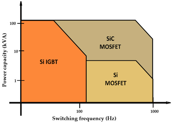
Figure 2. Comparison of the operating power and frequency for Si and SiC transistors (IGBT and MOSFET).
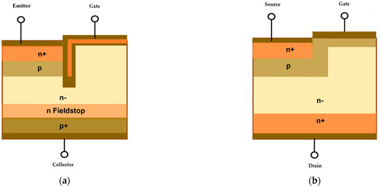
Figure 3. Schematic diagrams for; (a) Si IGBT and (b) SiC MOSFET.
One of the fundamental lifecycle evaluation factors of power switching semiconductor devices is their junction temperature and its fluctuation, since this affects their lifetime, which may cause device failure [29]. Junction temperature refers to the mean surface temperature on the SiC MOSFET chip or the absolute maximum temperature of the emitter metallization on the Si IGBT chip. It is influenced by several factors. For instance, in a multilayer IGBT module that handles a wide range of input supplies, any random input voltage fluctuation causes the module to repeatedly hold up the thermal cycle’s shock for an extended period. Thus, junction temperature also fluctuates during this thermal cycle, giving rise to alternating thermal stress. Similarly, for SiC MOSFET, thermal stress influences the junction temperature variation due to high switching frequency [30]. In general, when there is a degradation in electron mobility, a further increase in power generation will also increase the junction temperature of these devices due to power dissipation. On the other hand, the aging of the solder layer can also contribute to an increase in thermal resistance, which in turn raises the junction temperature of the power switching semiconductor chips [31,32]. The internal structure of these semiconductor devices and the comparison are discussed in the subsequent paragraph.
Considering Figure 3a, the trench gate structure of Si IGBT that runs through the n+-emitter and p-base regions facilitates an increase in the channel density and eliminates the usual channel voltage drop inherent to junction MOSFETs. Moreover, the IGBT chip thickness is reduced by introducing an “n-fieldstop” layer that lowers the static and dynamic losses. Conversely, the conventional planar structure of SiC MOSFET, illustrated in Figure 3b, has the n+ substrate region in contact with the drain electrode at the bottom of the device instead of the collector. In contrast to the structure of the IGBT, the emitter is replaced with the source electrode, while the gate electrode remains separated at the top by the interlayer insulator without a trench. Like Si IGBT, the channel of SiC MOSFET is located in the p region, between the n+ source and the n-layer. Although both devices’ structure is similar to the MOS-gated structure, there is no parasitic body diode in Si IGBT, and thus it requires an antiparallel Si p-i-n freewheeling diode for practical applications [33,34].
From the electrothermal behavior viewpoint, both devices are conducting to the top or bottom surface of the die when there is a current flow. This causes variation in the temperature distribution within the device, and thermal modeling of these devices under the same current and voltage rating has shown that the junction temperature and the temperature swing of IGBT are higher than that of SiC MOSFET, since the on-state resistance of the IGBT is independent of junction temperature [35]. Meanwhile, in case of short circuit failure, the junction temperature rises faster in SiC MOSFET than in IGBT, which results in a lower short circuit holding time. This is because the heat generation rate in SiC is three times higher than the conduction rate, when compared to Si IGBTs. Hence, during a short circuit, junction temperature will be dominated by the heat generation rate [36], suggesting that the magnitude of the junction temperature for both devices depends on their operation state. The structure of both devices is similar to traditional MOSFET, and since both are Si-based semiconductors, they are suitable for the TSOP junction temperature sensing approach. Moreover, since FBG could be bonded on SiC and IGBT devices while IRC can detect temperature distribution on their respective surfaces, both allow measurement of device junction temperature, thus making the OBS technique an attractive technology.
This entry is adapted from the peer-reviewed paper 10.3390/mi14081636
This entry is offline, you can click here to edit this entry!