Solid oxide fuel cells (SOFCs) are amongst the most widely used renewable alternative energy systems with near-zero carbon emission, high efficiency, and environment-friendly features. However, the high operating temperature of SOFCs is still considered a major challenge due to several issues regarding the materials’ corrosion, unwanted reactions between layers, etc. Thus, low-temperature SOFCs (LT-SOFCs) have gained significant interest during the past decades. Despite the numerous advantages of LT-SOFCs, material selection for each layer is of great importance as the common materials have not shown a desirable performance so far. In addition to the selection of the materials, fabrication techniques have a great influence on the properties of the SOFCs. As SOFCs with thinner layers showed lower polarisation resistance, especially in the electrolyte layer, different thin-film fabrication methods have been employed, and their effect on the overall performance of SOFCs has been evaluated.
- solid oxide fuel cells
- low-temperature SOFCs
- materials selection
- thin film
1. Introduction
Fuel cells are electrochemical devices that convert chemical energy into electricity with low emissions [1]. Since fuel cells do not have the limitations of internal combustion engines (Carnot cycle), they can generate electricity with higher efficiency [2]. In addition, the progressive increase in utilising hydrogen as a clean energy carrier has caused a great interest in developing more efficient fuel cells as a prospective power source by both research and manufacturing communities. In this regard, fuel cells have already shown great potential in providing electricity for rural areas with no or limited access to the public grid, removing the huge cost of wiring and electricity transfer to these areas [3][4].
According to the choice of fuel and electrolyte, fuel cells are categorised into six major groups: (1) alkaline fuel cell (AFC) [5], (2) phosphoric acid fuel cell (PAFC) [6], (3) solid oxide fuel cell (SOFC) [7], (4) molten carbonate fuel cell (MCFC) [8], (5) proton exchange membrane fuel cell (PEMFC) [9], and (6) direct methanol fuel cell (DMFC) [10]. SOFCs show promising properties compared to other types. SOFCs are among the most promising fuel cells in providing efficient electric power generation and substantial environmental benefits in case of a high level of fuel flexibility. It is this fuel flexibility that has made it possible to operate SOFCs on today’s conventional hydrocarbon fuels, such as methane, methanol, and ethanol [11]. It should be mentioned that anode, cathode, and electrolyte materials differ from one fuel cell technology to another. For example, polybenzimidazole (PBI) and Nafion are the most common membrane materials in PEMFCs, yttria-stabilised zirconia (YSZ), gadolinium-doped ceria (GDC), and lanthanum strontium gallium magnesium oxide (LSGM) are the most common electrolyte materials in SOFCs, molten potassium and lithium carbonate are the most common electrolyte materials in MCFCs, etc. Several anode and cathode materials can also be mentioned for each fuel cell technology, including Ni/GDC, LSCF, lithium metatitanate, porous Ni, and Pt [9][12][13]. Nonetheless, further development is required to overcome some existing limitations surrounding common fuel cell technologies. Reducing cost, improving durability, and further optimising performance have been the focus of most fuel cell research at the individual cell level, stack level, and general system level [14].
2. Ceramic Processing Techniques
2.1. Thin-Film Fabrication Methods
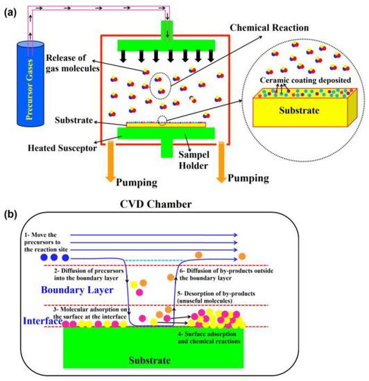
2.1.1. Chemical Vapour Deposition (CVD) Process
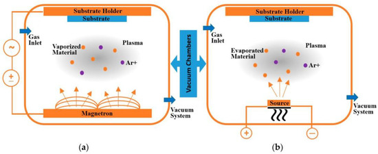
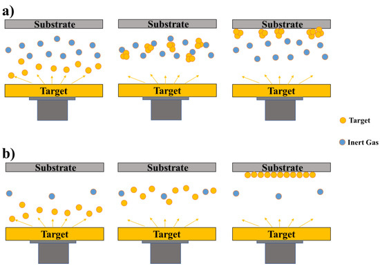
2.1.2. Physical Vapour Deposition (PVD) Process
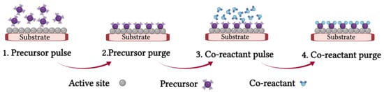
2.1.3. Atomic Layer Deposition (ALD) Process
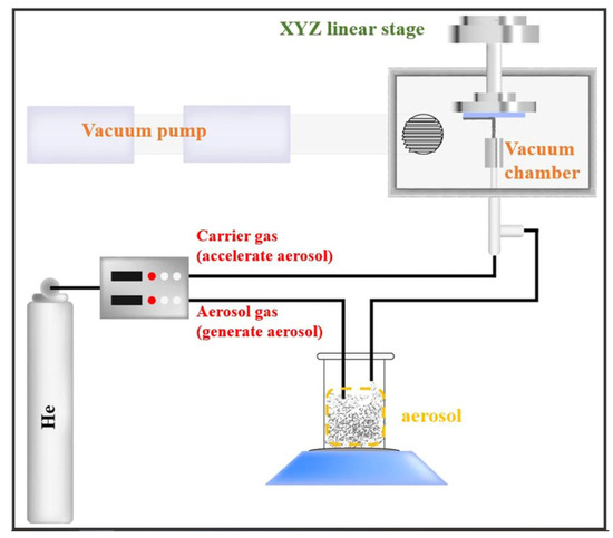
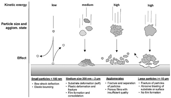
2.1.4. Aerosol Deposition (AD) Process
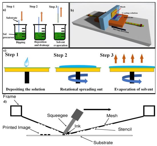
2.1.5. Dip Coating Process
2.1.6. Tape Casting Process
2.1.7. Spin Coating Process
2.1.8. Screen Printing Process
2.2. Other Fabrication Methods
2.2.1. Solid-State Reaction
2.2.2. Sol–Gel Process
2.2.3. Coprecipitation Process
2.2.4. Glycine Nitrate Process (Combustion)
This entry is adapted from the peer-reviewed paper 10.3390/cryst13071008
References
- Ilbas, M.; Kumuk, B. Numerical Modelling of a Cathode-Supported Solid Oxide Fuel Cell (SOFC) in Comparison with an Electrolyte-Supported Model. J. Energy Inst. 2019, 92, 682–692.
- Li, R.; Peng, L.; Wang, X.; Yang, J.; Yan, D.; Pu, J.; Chi, B.; Li, J. Investigating the Performance of Glass/Al2O3 Composite Seals in Planar Solid Oxide Fuel Cells. Compos. Part B Eng. 2020, 192, 107984.
- Baldi, F.; Wang, L.; Pérez-fortes, M.; Maréchal, F. A Cogeneration System Based on Solid Oxide and Proton Exchange Membrane Fuel Cells With Hybrid Storage for Off-Grid Applications. Front. Energy Res. 2019, 6, 139.
- Vostakola, M.F.; Salamatinia, B.; Horri, B.A. A Review on Recent Progress in the Integrated Green Hydrogen Production Processes. Energies 2022, 15, 1209.
- Wang, J.; Zhang, X.; Li, Y.; Liu, P.; Chen, X.; Zhang, P.; Wang, Z.; Liu, X. Sweet Drinks as Fuels for an Alkaline Fuel Cell with Nonprecious Catalysts. Energies 2021, 14, 206.
- Abderezzak, B. Introduction to Hydrogen Technology. In Introduction to Transfer Phenomena in PEM Fuel Cell; ISTE Press-Elsevier: London, UK, 2018; pp. 1–51.
- Study, A.F.; Hu, H.; Zou, J.; Shan, L.; Jiang, X.; Ni, Y.; Li, X.; Qian, X. Conductivities in Yttrium-Doped Barium Zirconate: A First-Principles Study. Crystals 2023, 13, 401.
- Recirculation, G.; Bian, J.; Duan, L.; Yang, Y. Simulation and Economic Investigation of CO2 Separation from Gas Turbine Exhaust Gas by Molten Carbonate Fuel Cell with Exhaust Gas Recirculation and Selective Exhaust Gas Recirculation. Energies 2023, 16, 3511.
- Hooshyari, K.; Amini Horri, B.; Abdoli, H.; Fallah Vostakola, M.; Kakavand, P.; Salarizadeh, P. A Review of Recent Developments and Advanced Applications of High-Temperature Polymer Electrolyte Membranes for PEM Fuel Cells. Energies 2021, 14, 5440.
- Rabissi, C.; Zago, M.; Bresciani, F.; Gazdzicki, P.; Casalegno, A. A Novel Accelerated Stress Test for a Representative Enhancement of Cathode Degradation in Direct Methanol Fuel Cells. Energies 2023, 16, 3226.
- Weber, A. Fuel Flexibility of Solid Oxide Fuel Cells. Fuel Cells 2021, 21, 440–452.
- Ng, K.H.; Rahman, H.A.; Somalu, M.R. Review: Enhancement of Composite Anode Materials for Low-Temperature Solid Oxide Fuels. Int. J. Hydrogen Energy 2019, 44, 30692–30704.
- Das, S.; Dutta, K.; Nessim, G.D.; Kader, M.A. Introduction to Direct Methanol Fuel Cells. In Direct Methanol Fuel Cell Technology; Elsevier: Amsterdam, The Netherlands, 2020; pp. 1–12. ISBN 9780128191583.
- Ali, M.; Hassan, W.; El Haj, M.; Allagui, A.; Cha, S.W. On the Technical Challenges a Ff Ecting the Performance of Direct Internal Reforming Biogas Solid Oxide Fuel Cells. Renew. Sustain. Energy Rev. 2019, 101, 361–375.
- Taroco, H.A.; Santos, J.A.F.; Domingues, R.Z.; Matencio, T. Ceramic Materials for Solid Oxide Fuel Cells. In Advances in Ceramics-Synthesis and Characterization, Processing and Specific Applications; Sikalidis, C., Ed.; IntechOpen: Minas Gerais, Brazil, 2011; pp. 423–446.
- Pianko-Oprych, P.; Jaworski, Z.; Kendall, K. Cell, Stack and System Modelling. In High-temperature Solid Oxide Fuel Cells for the 21st Century; Academic Press: Cambridge, MA, USA, 2016; pp. 407–460. ISBN 9780124104532.
- Zhang, J.; Lenser, C.; Menzler, N.H.; Guillon, O. Comparison of Solid Oxide Fuel Cell (SOFC) Electrolyte Materials for Operation at 500 °C. Solid State Ionics 2020, 344, 115138.
- Wang, J. Barriers of Scaling-up Fuel Cells: Cost, Durability and Reliability. Energy 2015, 80, 509–521.
- Wang, J. System Integration, Durability and Reliability of Fuel Cells: Challenges and Solutions. Appl. Energy 2017, 189, 460–479.
- Ding, D.; Li, X.; Lai, Y.; Liu, M. Enhancing SOFC Cathode Performance by Surface Modification through Infiltratio. Energy Environ. Sci. 2014, 7, 552–575.
- Bi, L.; Traversa, E. Synthesis Strategies for Improving the Performance of Doped-BaZrO3 Materials in Solid Oxide Fuel Cell Applications. J. Mater. Res. 2014, 29, 1–15.
- Munira, S.; Hafiz, M.; Othman, D.; Rahman, M.A.; Jaafar, J.; Ismail, A.F.; Li, K. Recent Fabrication Techniques for Micro-Tubular Solid Oxide Fuel Cell Support: A Review. J. Eur. Ceram. Soc. 2015, 35, 1–22.
- Jiang, S.P. Development of Lanthanum Strontium Cobalt Ferrite Perovskite Electrodes of Solid Oxide Fuel Cells—A Review. Int. J. Hydrogen Energy 2019, 44, 7448–7493.
- Huang, N.; Han, B.; Wang, Y.; Li, Y.; Su, Y.; Guan, W.; Zhou, X.; Chai, M.; Singhal, S.C. On the Dependence of Interfacial Resistance on Contact Materials between Cathode and Interconnect in Solid Oxide Fuel Cells. Int. J. Hydrogen Energy 2021, 46, 20078–20086.
- He, S.; Jiang, S.P. Electrode/Electrolyte Interface and Interface Reactions of Solid Oxide Cells: Recent Development and Advances. Prog. Nat. Sci. Mater. Int. 2021, 31, 341–372.
- Santoni, F.; Silva Mosqueda, D.M.; Pumiglia, D.; Viceconti, E.; Conti, B.; Boigues Muñoz, C.; Bosio, B.; Ulgiati, S.; McPhail, S.J. In-Situ Study of the Gas-Phase Composition and Temperature of an Intermediate-Temperature Solid Oxide Fuel Cell Anode Surface Fed by Reformate Natural Gas. J. Power Sources 2017, 370, 36–44.
- Su, H.; Hu, Y.H. Progress in Low-Temperature Solid Oxide Fuel Cells with Hydrocarbon Fuels. Chem. Eng. J. 2020, 402, 126235.
- Liu, J.; Zhu, C.; Zhu, D.; Jia, X.; Zhang, Y.; Yu, J.; Li, X.; Yang, M. High Performance Low-Temperature Solid Oxide Fuel Cells Based on Nanostructured Ceria-Based Electrolyte. Nanomaterials 2021, 11, 2231.
- Zarabi, S.; Imran, M.; Lund, P.D. A Review on Solid Oxide Fuel Cell Durability: Latest Progress, Mechanisms, and Study Tools. Renew. Sustain. Energy Rev. 2022, 161, 112339.
- Prakash, B.S.; Pavitra, R.; Kumar, S.S.; Aruna, S.T. Electrolyte Bi-Layering Strategy to Improve the Performance of an Intermediate Temperature Solid Oxide Fuel Cell: A Review. J. Power Sources 2018, 381, 136–155.
- Afzal, M.; Raza, R.; Du, S.; Lima, R.B.; Zhu, B. Synthesis of Ba0.3Ca0.7Co0.8Fe0.2O3-δ Composite Material as Novel Catalytic Cathode for Ceria-Carbonate Electrolyte Fuel Cells. Electrochim. Acta 2015, 178, 385–391.
- Eric, D. Wachsman; Kang Taek Lee Lowering the Temperature of Solid Oxide Fuel Cells. Science 2011, 334, 928–935.
- Gao, Z.; Mogni, L.; Miller, E.C.; Railsback, J.; Barnett, S.A. A Perspective on Low-Temperature Solid Oxide Fuel Cells. Energy Environ. Sci. 2016, 9, 1602–1644.
- Coddet, P.; Liao, H.; Coddet, C. A Review on High Power SOFC Electrolyte Layer Manufacturing Using Thermal Spray and Physical Vapour Deposition Technologies. Adv. Manuf. 2014, 2, 212–221.
- Liang, F.; Yang, J.; Zhao, Y.; Zhou, Y.; Yan, Z.; He, J.; Yuan, Q.; Wu, J.; Liu, P.; Zhong, Z.; et al. A Review of Thin Film Electrolytes Fabricated by Physical Vapor Deposition for Solid Oxide Fuel Cells. Int. J. Hydrogen Energy 2022, 47, 36926–36952.
- Horri, B.A.; Selomulya, C.; Wang, H. Electrochemical Characteristics and Performance of Anode-Supported SOFCs Fabricated Using Carbon Microspheres as a Pore-Former. Int. J. Hydrogen Energy 2012, 37, 19045–19054.
- Kharton, V.V.; Marques, F.M.B.; Atkinson, A. Transport Properties of Solid Oxide Electrolyte Ceramics: A Brief Review. Solid State Ionics 2004, 174, 135–149.
- Lamy, C.; Millet, P. A Critical Review on the Definitions Used to Calculate the Energy Efficiency Coefficients of Water Electrolysis Cells Working under near Ambient Temperature Conditions. J. Power Sources 2020, 447, 227350.
- Welaya, Y.M.A.; Mosleh, M.; Ammar, N.R. Thermodynamic Analysis of a Combined Gas Turbine Power Plant with a Solid Oxide Fuel Cell for Marine Applications. Int. J. Nav. Archit. Ocean Eng. 2013, 5, 529–545.
- Ouyang, T.; Zhao, Z.; Lu, J.; Su, Z.; Li, J. Waste Heat Cascade Utilisation of Solid Oxide Fuel Cell for Marine Applications. J. Clean. Prod. 2020, 275, 124133.
- Micoli, L.; Russo, R.; Coppola, T.; Pietra, A. Performance Assessment of the Heat Recovery System of a 12 MW SOFC-Based Generator on Board a Cruise Ship through a 0D Model. Energies 2023, 16, 3334.
- Fallah Vostakola, M.; Amini Horri, B. Progress in Material Development for Low-Temperature Solid Oxide Fuel Cells: A Review. Energies 2021, 14, 1280.
- Shina, J.W.; Go, D.; Kye, S.H.; Leea, S.; An, J. Review on Process-Microstructure-Performance Relationship in ALD- Engineered SOFCs. J. Phys. Energy 2019, 1, 042002.
- Frishberg, I. V Gas-Phase Method of Metal Powder Production. In Handbook of Non-Ferrous Metal Powders; Elsevier Ltd.: Yekaterinburg, Russia, 2019; Volume 1, pp. 187–200. ISBN 9780081005439.
- Sarangan, A. Nanofabrication. In Fundamentals and Applications of Nanophotonics; Woodhead Publishing: Dayton, OH, USA, 2016; pp. 149–184. ISBN 9781782424642.
- Igumenov, I.K.; Lukashov, V. V Modern Solutions for Functional Coatings in CVD Processes. Coatings 2022, 12, 1265.
- Carlsson, J.; Martin, P.M. Chemical Vapor Deposition. In Handbook of Deposition Technologies for Films and Coatings; William Andrew: Norwich, NY, USA, 2010; pp. 314–363.
- Sabzi, M.; Anijdan, S.H.M.; Shamsodin, M.; Farzam, M.; Hojjati-Najafabadi, A.; Feng, P.; Park, N.; Lee, U. A Review on Sustainable Manufacturing of Ceramic-Based Thin Films by Chemical Vapor Deposition (CVD): Reactions Kinetics and the Deposition Mechanisms. coatings 2023, 13, 188.
- Choi, H.R.; Neoh, K.C.; Choi, H.J.; Han, G.D.; Jang, D.Y.; Kim, D.; Shim, J.H. Nanoporous Silver Cathode Surface-Treated by Aerosol-Assisted Chemical Vapor Deposition of Gadolinia-Doped Ceria for Intermediate-Temperature Solid Oxide Fuel Cells. J. Power Sources 2018, 402, 246–251.
- Jang, D.Y.; Kim, M.; Kim, J.W.; Bae, K.; Son, J.; Schlupp, M.V.F.; Shim, J.H. High Performance Anode-Supported Solid Oxide Fuel Cells with Thin Film Yttria-Stabilized Zirconia Membrane Prepared by Aerosol-Assisted Chemical Vapor Deposition. J. Electrochem. Soc. 2017, 164, F484–F490.
- Sakai, T.; Kato, T.; Tanaka, Y.; Goto, T. Preparation of an Yttria-Stabilized Zirconia Electrolyte on a Porous Ni-Based Cermet Substrate by Laser Chemical Vapor Deposition. Mater. Today Commun. 2022, 33, 104169.
- Sawka, A.; Kwatera, A. Low Temperature Synthesis of Y2O3–Doped CeO2 Layers Using MOCVD. Mater. Sci. Eng. B 2022, 276, 115580.
- Sawka, A. Chemical Vapour Deposition of Scandia-Stabilised Zirconia Layers on Tubular Substrates at Low Temperatures. Materials 2022, 15, 2120.
- Sawka, A. MOCVD Growth of Gadolinium Oxide Layers on Tubes. Ceram. Int. J. 2023, 49, 23835–23843.
- Lee, Y.H.; Chang, I.; Cho, G.Y.; Park, J.; Yu, W.; Tanveer, W.H.; Cha, S.W. Thin Film Solid Oxide Fuel Cells Operating Below 600 ℃: A Review. Int. J. Precis. Eng. Manuf. Technol. 2018, 5, 441–453.
- Zhang, Y.; Knibbe, R.; Sunarso, J.; Zhong, Y.; Zhou, W.; Shao, Z. Recent Progress on Advanced Materials for Solid-Oxide Fuel Cells Operating Below 500 °C. Adv. Mater. 2017, 29, 1700132.
- Pinto, G. Sputtering Physical Vapour Deposition (PVD) Coatings: ACritical Review on Process Improvement AndMarket Trend Demands. Coatings 2018, 8, 402.
- Seshan, K.; Schepis, D. Handbook of Thin Film Deposition, 4th ed.; Seshan, K., Globalfoundries, D.S., Eds.; William Andrew: Norwich, NY, USA, 2018; ISBN 9780128123126.
- Infortuna, B.A.; Harvey, A.S.; Gauckler, L.J. Microstructures of CGO and YSZ Thin Films by Pulsed Laser Deposition. Adv. Funct. Mater. 2008, 18, 127–135.
- Coppola, N.; Polverino, P.; Carapella, G.; Ciancio, R.; Rajak, P.; Dario, M.; Martinelli, F.; Maritato, L.; Pianese, C. Large Area Deposition by Radio Frequency Sputtering of Gd0.1Ce0.9O1.95 Buffer Layers in Solid Oxide Fuel Cells: Structural, Morphological and Electrochemical Investigation. Materials (Basel) 2021, 14, 5826.
- Mattox, D.M. Handbook of Physical Vapor Deposition (PVD) Processing, 2nd ed.; William Andrew: Norwich, NY, USA, 2010; ISBN 9780815520375.
- Lamas, J.S.; Leroy, W.P.; Depla, D. Influence of Target–Substrate Distance and Composition on the Preferential Orientation of Yttria-Stabilized Zirconia Thin Films. Thin Solid Films 2012, 520, 4782–4785.
- Nédélec, R.; Uhlenbruck, S.; Sebold, D.; Haanappel, V.A.C.; Buchkremer, H.; Stöver, D. Dense Yttria-Stabilised Zirconia Electrolyte Layers for SOFC by Reactive Magnetron Sputtering. J. Power Sources 2012, 205, 157–163.
- Vafaeenezhad, S.; Hanifi, A.R.; Laguna-bercero, M.A.; Etsell, T.H. Microstructure and Long-Term Stability of Ni–YSZ Anode Supported Fuel Cells: A Review To. Mater. Futur. 2022, 1, 042101.
- Hanifi, A.R.; Shinbine, A.; Etsell, T.H. Development Of Monolithic YSZ Porous and Dense Layers through Multiple Slip Casting for Ceramic Fuel Cell Applications. Int. J. Appl. Ceram. Technol. 2012, 9, 1011–1021.
- Fonseca, F.C.; Uhlenbruck, S.; Nédélec, R.; Sebold, D.; Buchkremer, H.P. Temperature and Bias Effects on Sputtered Ceria Diffusion Barriers for Solid Oxide Fuel Cells. J. Electrochem. Soc. 2010, 157, B1515–B1519.
- Ostadi, A.; Hosseini, S.H.; Fordoei, M.E. The Effect of Temperature and Roughness of the Substrate Surface on the Microstructure and Adhesion Strength of EB-PVD ZrO2-%8wtY2O3 Coating. Ceram. Int. 2020, 46, 2287–2293.
- Tanhaei, M.; Mozammel, M. Yttria-Stabilized Zirconia Thin Film Electrolyte Deposited by EB-PVD on Porous Anode Support for SOFC Applications. Ceram. Int. 2017, 43, 3035–3042.
- Shim, J.H.; Han, G.D.; Choi, H.J.; Kim, Y.; Xu, S.; An, J.; Kim, Y.B.; Graf, T.; Schladt, T.D.; Gür, T.M.; et al. Atomic Layer Deposition for Surface Engineering of Solid Oxide Fuel Cell Electrodes. Int. J. Precis. Eng. Manuf.-Green Technol. 2019, 6, 629–646.
- Lee, S.; Lee, Y.; Park, J.; Yu, W.; Cho, G.Y.; Kim, Y.; Cha, S.W. Effect of Plasma-Enhanced Atomic Layer Deposited YSZ Inter-Layer on Cathode Interface of GDC Electrolyte in Thin Film Solid Oxide Fuel Cells. Renew. Energy 2019, 144, 123–128.
- Shin, J.W.; Oh, S.; Lee, S.; Yu, J.G.; Park, J.; Go, D.; Yang, B.C.; Kim, H.J.; An, J. Ultrathin Atomic Layer-Deposited CeO2 Overlayer for High-Performance Fuel Cell Electrodes. ACS Appl. Mater. Interfaces 2019, 11, 46651–46657.
- Ahn, C.H.; Kim, S.H.; Yun, M.G.; Cho, H.K. Design of Step Composition Gradient Thin Film Transistor Channel Layers Grown by Atomic Layer Deposition. Appl. Phys. Lett. 2014, 105, 223513.
- Knoops, H.C.M.; Potts, S.E.; Bol, A.A.; Kessels, W.M.M. Atomic Layer Deposition. In Handbook of Crystal Growth: Thin Films and Epitaxy, 2nd ed.; Elsevier B.V.: Eindhoven, The Netherlands, 2015; pp. 1101–1134. ISBN 9780444633057.
- Shahmohammadi, M.; Mukherjee, R.; Sukotjo, C.; Diwekar, U.M.; Takoudis, C.G. Recent Advances in Theoretical Development of Thermal Atomic Layer Deposition: A Review. Nanomaterials 2022, 12, 831.
- Shim, J.H.; Choi, H.J.; Kim, Y.; Torgersen, J.; An, J.; Lee, M.H.; Prinz, F.B. Process-Property Relationship in High-K ALD SrTiO3 and BaTiO3: A Review. J. Mater. Chem. C 2017, 5, 8000–8013.
- Detavernier, C.; Dendooven, J.; Sree, S.P.; Ludwigc, K.F.; Martens, J.A. Tailoring Nanoporous Materials by Atomic Layer Deposition. Chem. Soc. Rev. 2011, 40, 5242–5253.
- Koponen, S.E.; Gordon, P.G.; Barry, S.T. Principles of Precursor Design for Vapour Deposition Methods. Polyhedron 2016, 108, 59–66.
- Putkonen, B.M.; Sajavaara, T.; Johansson, L.; Niinistö, L. Low-Temperature ALE Deposition of Y2O3 Thin Films from β-Diketonate Precursors**. Chem. Vap. Depos. 2001, 7, 44–50.
- Hausmann, D.M.; Kim, E.; Becker, J.; Gordon, R.G. Atomic Layer Deposition of Hafnium and Zirconium Oxides Using Metal Amide Precursors. Chem. Mater. 2002, 14, 4350–4358.
- Cassir, M.; Putkonen, M.; Niinisto, L. Electrical Properties of Thin Yttria-Stabilized Zirconia Overlayers Produced by Atomic Layer Deposition for Solid Oxide Fuel Cell Applications. Appl. Surf. Sci. 2007, 253, 3962–3968.
- Kerman, K.; Lai, B.-K.; Ramanathan, S. Nanoscale Compositionally Graded Thin-Film Electrolyte Membranes for Low-Temperature Solid Oxide Fuel Cells. Adv. Energy Mater. 2012, 2, 656–661.
- Baek, J.D.; Yu, C.; Su, P. A Silicon-Based Nanothin Film Solid Oxide Fuel Cell Array with Edge Reinforced Support for Enhanced Thermal Mechanical Stability. Nano Lett. 2016, 16, 2413–2417.
- Shim, J.H.; Chao, C.-C.; Huang, H.; Prinz, F.B. Atomic Layer Deposition of Yttria-Stabilized Zirconia for Solid Oxide Fuel Cells. Chem. Mater. 2007, 19, 3850–3854.
- Lee, C.; Cho, M.-Y.; Kim, M.; Jang, J.; Oh, Y.; Oh, K.; Kim, S.; Park, B.; Kim, B.; Koo, S.-M.; et al. Applicability of Aerosol Deposition Process for Flexible Electronic Device and Determining the Film Formation Mechanism with Cushioning Effects. Sci. Rep. 2019, 9, 2166.
- Erilin, I.S.; Agarkov, D.A.; Burmistrov, I.N.; Pukha, V.E.; Yalovenko, D.V.; Lyskov, N.V.; Levin, M.N.; Bredikhin, S.I. Aerosol Deposition of Thin-Film Solid Electrolyte Membranes for Anode-Supported Solid Oxide Fuel Cells. Mater. Lett. 2020, 266, 127439.
- Bredikhin, S.I.; Agarkov, D.A.; Agarkova, E.A.; Burmistrov, I.N.; Cherkasov, A.M.; Pukha, V.E.; Yalovenko, D.V.; Lyskov, N.V. Aerosol Deposition as a Promising Technique to Fabricating a Thin-Film Solid Electrolyte of Solid Oxide Fuel Cells. ECS Trans. 2019, 91, 403–413.
- Hanft, D.; Exner, J.; Schubert, M.; Stöcker, T.; Fuierer, P.; Moos, R. An Overview of the Aerosol Deposition Method: Process Fundamentals and New Trends in Materials Applications. J. Ceram. Sci. Technol. 2015, 182, 147–182.
- Akedo, J.; Ichiki, M.; Kikuchi, K.; Maeda, R. Jet Molding System for Realization of Three-Dimensional Micro-Structures. Sens. Actuators A 1998, 69, 106–112.
- Akedo, J.; Lebedev, M. Microstructure and Electrical Properties of Lead Zirconate Titanate (Pb(Zr52/Ti48)O3) Thick Films Deposited by Aerosol Deposition Method. Jpn. J. Appl. Phys. 1999, 38, 5397.
- Akedo, J. Room Temperature Impact Consolidation (RTIC) of Fine Ceramic Powder by Aerosol Deposition Method and Applications to Microdevices. J. Therm. Spray Technol. 2008, 17, 181–198.
- Furuya, Y.; Tanaka, M.; Kitaoka, S.; Hasegawa, M. Method for Determining Particle Velocity during Aerosol Deposition by Impact Pressure of the Particles. Surf. Coat. Technol. 2022, 443, 128616.
- Furuya, Y.; Konuma, S.; Hasegawa, M. Deposition Mechanism of Alumina Particles in Aerosol Deposition Based on the Kinetic Energy of Particles. Surf. Coat. Technol. 2023, 458, 129362.
- Kuroyanagi, S.; Shinoda, K.; Yumoto, A.; Akedo, J. Size-Dependent Quasi Brittle–Ductile Transition of Single Crystalline Alpha-Alumina Particles during Microcompression Tests. Acta Mater. J. 2020, 195, 588–596.
- Yeganeh, A.Z.; Jadidi, M.; Moreau, C.; Dolatabadi, A. Surface & Coatings Technology Numerical Modeling of Aerosol Deposition Process. Surf. Coat. Technol. 2019, 370, 269–287.
- Matsubayashi, Y.; Akedo, J. Aerosol Deposition of Alumina Films on Microstructured Silicon Substrates. Ceram. Int. 2023, 49, 21570–21576.
- Schubert, M.; Exner, J.; Moos, R. Influence of Carrier Gas Composition on the Stress of Al2O3 Coatings Prepared by the Aerosol Deposition Method. Materials 2014, 7, 5633–5642.
- Seto, N.; Endo, K.; Sakamoto, N.; Hirose, S.; Akedo, J. Hard A-Al2O3 Film Coating on Industrial Roller Using Aerosol Deposition Method. J. Therm. Spray Technol. 2014, 23, 1373–1381.
- Lee, W.; Kim, H.; Lee, D.; Jeong, M.; Lim, D.; Nam, S. Al2O3-Nanodiamond Composite Coatings with High Durability and Hydrophobicity Prepared by Aerosol Deposition. Surf. Coat. Technol. 2012, 206, 4679–4684.
- Xiao, Y.; Wang, M.; Bao, D.; Wang, Z.; Jin, F.; Wang, Y.; He, T. Performance of Fuel Electrode-Supported Tubular Protonic Ceramic Cells Prepared through Slip Casting and Dip-Coating Methods. Catalysts 2023, 13, 182.
- Winter, R.L.; Singh, P.; King, M.K., Jr.; Mahapatra, M.K.; Sampathkumaran, U. Protective Ceramic Coatings for Solid Oxide Fuel Cell (SOFC) Balance-of-Plant Components. Adv. Mater. Sci. Eng. 2018, 2018, 9121462.
- Lei, L.; Bai, Y.; Liu, Y. An Investigation on Dip-Coating Technique for Fabricating Anode-Supported Solid Oxide Fuel Cells. Int. J. Appl. Ceram. Technol. 2015, 12, 351–357.
- Sahu, S.K.; Panthi, D.; Soliman, I.; Feng, H.; Du, Y. Fabrication and Performance of Micro-Tubular Solid Oxide Cells. Energies 2022, 15, 3536.
- Exploration, C.A.B.; Butt, M.A. Thin-Film Coating Methods: A Successful Marriage of High-Quality and Cost-Effectiveness—A Brief Exploration. Coatings 2022, 12, 1115.
- Panthi, D.; Tsutsumi, A. A Novel Multistep Dip-Coating Method for the Fabrication of Anode-Supported Microtubular Solid Oxide Fuel Cells. J. Solid State Electrochem. 2014, 18, 1899–1905.
- Niazmand, M.; Maghsoudipour, A.; Alizadeh, M.; Khakpour, Z.; Kariminejad, A. Effect of Dip Coating Parameters on Microstructure and Thickness of 8YSZ Electrolyte Coated on NiO-YSZ by Sol-Gel Process for SOFCs Applications. Ceram. Int. 2022, 48, 16091–16098.
- Delory, M.; Chorein, B.; Brulez, A.; Mees, L.; Grosjean, N.; Fiorani, T.; Benayoun, S. Role of Surface-Tension Additive in Coating Framing Effect Topography Mathilde. Colloids Surf. A Physicochem. Eng. Asp. 2023, 658, 130554.
- Phillips, C.O.; Beynon, D.G.; Hamblyn, S.M.; Davies, G.R.; Gethin, D.T.; Claypole, T.C. A Study of the Abrasion of Squeegees Used in Screen Printing and Its Effect on Performance with Application in Printed Electronics. Coatings 2014, 4, 356–379.
- Howatt, G.N.; Breckenridge, R.G.; Brownlow, J.M. Fabrication of Thin Ceramic Sheets for Capacitors. J. Am. Ceram. Soc. 1947, 30, 237–242.
- Nishihora, R.K.; Rachadel, P.L.; Quadri, M.G.N.; Hotza, D. Manufacturing Porous Ceramic Materials by Tape Casting—A Review. J. Eur. Ceram. Soc. 2018, 38, 988–1001.
- Nie, L.; Sun, Q.; Liu, Z.; Liu, M. Graded Porous Solid Oxide Fuel Cells Fabricated by Multilayer Tape Casting and Co-Firing Progress. Int. J. Hydrogen Energy 2015, 40, 16503–16508.
- Lee, S.; Lee, K.; Jang, Y.; Bae, J. Fabrication of Solid Oxide Fuel Cells (SOFCs) by Solvent-Controlled Co-Tape Casting Technique. Int. J. Hydrogen Energy 2017, 42, 1648–1660.
- Snowdon, A.L.; Steinberger-wilckens, R. Five-Layer Reverse Tape Casting of IT-SOFC. Int. J. Appl. Ceram. Technol. 2022, 19, 289–298.
- Transactions, E.C.S.; Society, T.E. Tubular Solid Oxide Fuel Cells Fabricated by Tape-Casting and Dip-Coating Methods. ECS Trans. 2019, 91, 329–337.
- Bulatova, R.; Jabbari, M.; Kaiser, A.; Negra, M.D.; Andersen, K.B.; Gurauskis, J.; Bahl, C.R.H. Thickness Control and Interface Quality as Functions of Slurry Formulation and Casting Speed in Side-by-Side Tape Casting. J. Eur. Ceram. Soc. 2014, 34, 4285–4295.
- Aishwarya, K.P.; Darve, R.; Gadde, J.R.; Kale, H. Optimisation of Slurry Compositions for Improving the Mechanical Properties of Low Temperature Co-Fired Ceramic (LTCC) Tapes To. IOP Conf. Ser. 2022, 1248, 012096.
- Varghese, J.; Joseph, N.; Jantunen, H. Multilayer Glass–Ceramic/Ceramic Composite Substrates. In Encyclopedia of Materials: Technical Ceramics and Glasses; Elsevier: Oulu, Finland, 2021; Volume 3, pp. 437–451. ISBN 9780128185421.
- Myung, J.; Jun, H.; Park, H.; Hwan, M.; Hyun, S. Fabrication and Characterization of Planar-Type SOFC Unit Cells Using the Tape-Casting/Lamination/Co-Firing Method. Int. J. Hydrogen Energy 2011, 37, 498–504.
- Santos, T.H.; Grilo, J.P.F.; Loureiro, F.J.A.; Fagg, D.P.; Fonseca, F.C.; Macedo, D.A. Structure, Densification and Electrical Properties of Gd3+ and Cu2+ Co- Doped Ceria Solid Electrolytes for SOFC Applications: Effects of Gd2O3 Content. Ceram. Int. 2018, 44, 2745–2751.
- Jabbari, M.; Bulatova, R.; Tok, A.I.Y.; Bahl, C.R.H.; Mitsoulis, E.; Hattel, J.H. Ceramic Tape Casting: A Review of Current Methods and Trends with Emphasis on Rheological Behaviour and Flow Analysis. Mater. Sci. Eng. B 2016, 212, 39–61.
- Coduri, M.; Checchia, S.; Longhi, M.; Ceresoli, D. Rare Earth Doped Ceria: The Complex Connection Between Structure and Properties. Front. Chem. 2018, 6, 526.
- Mahmud, L.S.; Muchtar, A. Challenges in Fabricating Planar Solid Oxide Fuel Cells: A Review. Renew. Sustain. Energy Rev. 2017, 72, 105–116.
- Mishra, A.; Bhatt, N.; Bajpai, A.K. Nanostructured Superhydrophobic Coatings for Solar Panel Applications. In Nanomaterials-Based Coatings; Elsevier Inc.: Jabalpur, India, 2019; pp. 397–424. ISBN 9780128158845.
- Yilbas, B.S.; Al-Sharafi, A.; Ali, H. Surfaces for Self-Cleaning. In Self-Cleaning of Surfaces and Water Droplet Mobility; Elsevier: Dhahran, Saudi Arabia, 2019; pp. 45–98. ISBN 9780128147764.
- Cui, Z.; Liao, L. Coating and Printing Processes. In Solution Processed Metal Oxide Thin Films for Electronic Applications; Elsevier Inc.: Changsha, China, 2020; pp. 83–97. ISBN 9780128149300.
- Zhang, J.X.J.; Hoshino, K. Fundamentals of Nano/ Microfabrication and Scale Effect. In Molecular Sensors and Nanodevices Principles, Designs and Applications in Biomedical Engineering; Academic Press: Cambridge, MA, USA, 2019; pp. 43–111. ISBN 9780128148624.
- Xu, X.; Xia, C.; Huang, S.; Peng, D. YSZ Thin Films Deposited by Spin-Coating for IT-SOFCs. Ceram. Int. 2005, 31, 1061–1064.
- Wang, J.; Lu, Z.; Chen, K.; Huang, X.; Ai, N.; Hu, J.; Zhang, Y.; Su, W. Study of Slurry Spin Coating Technique Parameters for the Fabrication of Anode-Supported YSZ Films for SOFCs Jiaming. J. Power Sources 2007, 164, 17–23.
- Chen, M.; Hee, B.; Xu, Q.; Guk, B.; Ping, D. Fabrication and Performance of Anode-Supported Solid Oxide Fuel Cells via Slurry Spin Coating. J. Memb. Sci. 2010, 360, 461–468.
- Yang, Q.; Wang, Y.; Tian, D.; Wu, H.; Ding, Y.; Lu, X.; Chen, Y.; Lin, B. Enhancing Performance and Stability of Symmetrical Solid Oxide Fuel Cells via Quasi-Symmetrical Ceria-Based Buffer Layers. Ceram. Int. 2022, 48, 27509–27515.
- Ramasamy, D.; Nasani, N.; Pukazhselvan, D.; Fagg, D.P. Increased Performance by Use of a Mixed Conducting Buffer Layer, Terbia-Doped Ceria, for Nd2NiO4þd SOFC/SOEC Oxygen Electrodes. Int. J. Hydrogen Energy 2019, 44, 31466–31474.
- Wu, Y.; Sang, J.; Liu, Z.; Fan, H.; Cao, B.; Wang, Q.; Yang, J.; Guan, W.; Liu, X.; Wang, J. Enhancing the Performance and Stability of Solid Oxide Fuel Cells by Adopting Samarium-Doped Ceria Buffer Layer. Ceram. Int. 2023, 49, 20290–20297.
- Feng, Z.; Zhang, X.; Luo, D. Evolution and Effect on Electrolysis Performance of Pores in YSZ Electrolyte Films Prepared by Screen-Printing. Ceram. Int. 2023, 49, 10731–10737.
- Baharuddin, N.A. Fabrication of High-Quality Electrode Films for Solid Oxide Fuel Cell by Screen Printing: A Review on Important Processing Parameters. Int. J. Energy Res. 2020, 44, 8296–8313.
- Graca, V.C.D.; Holz, L.I.V.; Loureiro, F.J.A.; Mikhalev, S.M.; Fagg, D.P. Ba2NiMoO6-δ as a Potential Electrode for Protonic Ceramic Electrochemical Cells. Int. J. Hydrogen Energy 2023.
- Tomašegovi, T. Properties and Colorimetric Performance of Screen-Printed Thermochromic/UV-Visible Fluorescent Hybrid Ink Systems. Appl. Sci. 2021, 11, 11414.
- Somalu, M.R.; Yufit, V.; Brandon, N.P. The Effect of Solids Loading on the Screen-Printing and Properties of Nickel/Scandia-Stabilized-Zirconia Anodes for Solid Oxide Fuel Cells. Int. J. Hydrogen Energy 2013, 38, 9500–9510.
- Mücke, R.; Büchler, O.; Menzler, N.H.; Lindl, B.; Vaßen, R.; Buchkremer, H.P. High-Precision Green Densities of Thick Films and Their Correlation with Powder, Ink, and Film Properties. J. Eur. Ceram. Soc. 2014, 34, 3897–3916.
- Von Dollen, P.; Barnett, S. A Study of Screen Printed Yttria-Stabilized Zirconia Layers for Solid Oxide Fuel Cells. J. Am. Ceram. Soc. 2005, 3368, 3361–3368.
- Potts, S.; Phillips, C.; Jewell, E.; Clifford, B.; Lau, Y.C.; Claypole, T. High-Speed Imaging the Effect of Snap-off Distance and Squeegee Speed on the Ink Transfer Mechanism of Screen-Printed Carbon Pastes. J. Coat. Technol. Res. 2020, 17, 447–459.
- Na, S.; Tio, B.; Chaou, F.; Bendahhou, A.; Chourti, K.; Jalafi, I.; Yahakoub, E.H.; El Barkany, S.; Abou-salama, M. Optimisation of Electrical Conductivity and Dielectric Properties of Sn4+-Doped (Na0.5Bi0.5)TiO3 Perovskite. Ceram. Int. 2023, 49, 17940–17952.
- Kaur, P.; Singh, K. Structural, Morphological and Conducting Properties of Copper and Nickel-Substituted Strontium Manganite. Mater. Today Commun. 2023, 35, 106056.
- Kim, D.; Taek, K. Effect of Lanthanide (Ln=La, Nd, and Pr) Doping on Electrochemical Performance of Ln2NiO4+δ−YSZ Composite Cathodes for Solid Oxide Fuel Cells. Ceram. Int. J. 2021, 47, 2493–2498.
- Chandrasekaran, R.E.G. Structural, Optical and Magnetic Characterization of Cu-Doped ZnO Nanoparticles Synthesized Using Solid State Reaction Method. J. Mater. Sci. Mater. Electron. 2010, 21, 1168–1173.
- Rafique, M.; Nawaz, H.; Rafique, M.S.; Tahir, M.B.; Nabi, G.; Khalid, N.R. Material and Method Selection for Efficient Solid Oxide Fuel Cell Anode: Recent Advancements and Reviews. Int. J. Energy Res. 2019, 43, 2423–2446.
- Yang, H.; Wu, N. Ionic Conductivity and Ion Transport Mechanisms Ofsolid-state Lithium-ion Battery Electrolytes: A Review. Energy Sci. Eng. 2022, 10, 1643–1671.
- Jiang, S.P. Solid-State Electrochemistry and Solid Oxide Fuel Cells: Status and Future Prospects. Electrochem. Energy Rev. 2022, 5, 5–21.
- Zhan, Z.; Wen, T.; Tu, H.; Lu, Z. AC Impedance Investigation of Samarium-Doped Ceria. J. Electrochem. Soc. 2001, 148, 427–432.
- Martinelli, H.; Lamas, D.G.; Leyva, A.G.; Sacanell, J. Influence of Particle Size and Agglomeration in Solid Oxide Fuel Cell Cathodes Using Manganite Nanoparticles. Mater. Res. Express 2018, 5, 075013.
- Tolchard, J.R.; Grande, T. Chemical Compatibility of Candidate Oxide Cathodes for BaZrO3 Electrolytes. Solid State Ionics 2007, 178, 593–599.
- Mehranjani, A.S.; Cumming, D.J.; Sinclair, D.C.; Rothman, R.H. Journal of the European Ceramic Society Low-Temperature Co-Sintering for Fabrication of Zirconia / Ceria Bi-Layer Electrolyte via Tape Casting Using a Fe2O3 Sintering Aid. J. Eur. Ceram. Soc. 2017, 37, 3981–3993.
- Mah, J.C.W.; Aznam, I.; Muchtar, A.; Somalu, M.R.; Raharjo, J. Synthesis of (Cu,Mn,Co)3O4 Spinel: Effects of Citrate-to-Nitrate Ratio on Its Homogeneity and Electrical Properties. Energies 2023, 16, 1382.
- Lian, Z.; Chen, F.; Song, X.; Liao, D.; Peng, K. Electrochemical Performance of Li13.9Sr0.1Zn(GeO4)4 Prepared by Sol-Gel for Solid Oxide Fuel Cell Electrolyte. J. Alloys Compd. 2021, 882, 160696.
- Rivai, A.K.; Shabrina, N.; Setiawan, A.R. Synthesis and Characterization of 8YSZ/5GDC Composite and Dissimiliar-Bulk by Sonochemistry Assisted Sol-Gel Method. J. Phys. Conf. Ser. 2017, 817, 012001.
- Cushing, B.L.; Kolesnichenko, V.L.; Connor, C.J.O. Recent Advances in the Liquid-Phase Syntheses of Inorganic Nanoparticles. Chem. Rev. 2004, 104, 3893–3946.
- Vostakola, M.F.; Yekta, B.E.; Mirkazemi, S.M. The Effects of Vanadium Pentoxide to Oxalic Acid Ratio and Different Atmospheres on the Formation of VO2 Nanopowders Synthesized via Sol–Gel Method. J. Electron. Mater. 2017, 46, 6689–6697.
- Shabani, S.; Naghizadeh, R.; Fallah Vostakola, M.; Golestanifard, F. The Effect of MgO Addition on the Properties of Alumina-Based Ceramic Cores Prepared via Sol–Gel Process. J. Sol-Gel Sci. Technol. 2020, 96, 539–549.
- Medina-Ramirez, I.; Hernandez-Ramirez, A.; Maya-Trevino, M.L. Synthesis Methods for Photocatalytic Materials. In Photocatalytic Semiconductors; Springer: Cham, Switzerland, 2015; pp. 69–102. ISBN 9783319109992.
- Hossain, S.; Abdalla, A.M.; Noorazean, S.; Jamain, B.; Hj, J. A Review on Proton Conducting Electrolytes for Clean Energy and Intermediate Temperature-Solid Oxide Fuel Cells. Renew. Sustain. Energy Rev. 2017, 79, 750–764.
- Navas, D.; Fuentes, S.; Castro-alvarez, A.; Chavez-Angel, E. Review on Sol-Gel Synthesis of Perovskite and Oxide Nanomaterials. Gels 2021, 7, 275.
- Huang, W.; Shuk, P.; Greenblatt, M. Properties of Sol-Gel Prepared Ce1-XSmxO2-x/2 Solid Electrolytes. Solid State Ionics 1997, 100, 23–27.
- Piñol, S.; Najib, M.; Bastidas, D.M.; Calleja, A.; Capdevila, X.G.; Segarra, M.; Espiell, F.; Ruiz-Morales, J.C.; Marrero-López, D.; Nuñez, P. Microstructure–Conductivity Relationship in Gd- and Sm-Doped Ceria-Based Electrolytes Prepared by the Acrylamide Sol–Gel-Related Method. J. Solid State Electrochem. 2004, 8, 650–654.
- Huang, K.; Feng, M.; Goodenough, J.B. Synthesis and Electrical Properties of Dense Ce0.9Gd0.1O1.95 Ceramics Keqin. J. Am. Ceram. Soc. 1998, 62, 357–362.
- Choolaei, M.; Jakubczyk, E.; Amini, B. Synthesis and Characterisation of a Ceria-Based Cobalt-Zinc Anode Nanocomposite for Low-Temperature Solid Oxide Fuel Cells (LT-SOFCs). Electrochim. Acta 2023, 445, 142057.
- Bellardita, M.; Di Paola, A.; Yurdakal, S.; Palmisano, L. Preparation of Catalysts and Photocatalysts Used for Similar Processes. In Heterogeneous Photocatalysis; Elsevier B.V.: Amsterdam, The Netherlands, 2019; pp. 25–56. ISBN 9780444640154.
- Lesani, P.; Babaei, A.; Ataie, A.; Mostafavi, E. Nanostructured MnCo2O4 Synthesized via Co-Precipitation Method for SOFC Interconnect Application. Int. J. Hydrogen Energy 2016, 41, 20640–20649.
- Teng, Y.; Zuhairi, A.; Amini, B.; Salamatinia, B. Synthesis and Characterisation of Y2O3 Using Ammonia Oxalate as a Precipitant in Distillate Pack Co-Precipitation Process. Ceram. Int. 2018, 44, 18693–18702.
- Liu, S.; Ma, C.; Ma, M.; Xu, F. Magnetic Nanocomposite Adsorbents. In Composite Nanoadsorbents; Elsevier Inc.: Shihezi, China, 2019; pp. 295–316. ISBN 9780128141328.
- Agli, G.D.; Spiridigliozzi, L.; Pansini, M.; Accardo, G.; Yoon, S.P.; Frattini, D. Effect of the Carbonate Environment on Morphology and Sintering Behaviour of Variously Co-Doped (Ca, Sr, Er, Pr) Samarium-Doped Ceria in Co- Precipitation/Hydrothermal Synthesis. Ceram. Int. 2018, 44, 17935–17944.
- Hui, Y.; Liu, B.; Li, J.; Jun, Y. Improved Energy Storage Performance of Ba0.4Sr0.6TiO3 Nanocrystalline Ceramics Prepared by Using Oxalate Co-Precipitation and Spark Plasma Sintering. Mater. Res. Bull. 2019, 113, 141–145.
- Teng, Y.; Zuhairi, A.; Amini, B.; Salamatinia, B. Optimised Co-Precipitation Synthesis Condition for Oxalate-Derived Zirconia Nanoparticles. Ceram. Int. 2019, 45, 22930–22939.
- Dong, H.; Koenig, G.M., Jr. A Review on Synthesis and Engineering of Crystal Precursors Produced Via Coprecipitation for Multicomponent Lithium-Ion Battery Cathode Materials. CrystEngComm 2020, 22, 1514–1530.
- Pelosato, R.; Cristiani, C.; Dotelli, G.; Mariani, M.; Donazzi, A.; Natali, I.; Leonardo, P. Co-Precipitation Synthesis of SOFC Electrode Materials. Int. J. Hydrogen Energy 2012, 38, 480–491.
- Choolaei, M.; Bull, T.; Reina, T.R.; Horri, B.A. Synthesis and Characterisation of Nanocrystalline CuO–Fe2O3/GDC Anode Powders for Solid Oxide Fuel Cells. Ceram. Int. 2020, 46, 14776–14786.
- Dokiya, M.; Horita, T.; Kawada, T.; Sakai, N.; Yokokawa, H. Low Temperature Fabrication of (Y,Gd,Sm)-Doped Ceria Electrolyte. Solid State Ionics 1996, 86–88, 1255–1258.
- Zha, S.; Xia, C.; Meng, G. Effect of Gd (Sm) Doping on Properties of Ceria Electrolyte for Solid Oxide Fuel Cells. J. Power Sources 2003, 115, 44–48.
- Jongen, N.; Bowen, P.; Lemaitre, J.; Valmalette, J.-C.; Hofmann, H. Precipitation of Self-Organized Copper Oxalate Polycrystalline Particles in the Presence of Hydroxypropylmethylcellulose (HPMC): Control of Morphology. J. Colloid Interface Sci. 2000, 226, 189–198.
- Huang, J.; Mao, Z.; Liu, Z.; Wang, C. Development of Novel Low-Temperature SOFCs with Co-Ionic Conducting SDC-Carbonate Composite Electrolytes. Electrochem. Commun. 2007, 9, 2601–2605.
- Huang, J.; Mao, Z.; Liu, Z.; Wang, C. Performance of Fuel Cells with Proton-Conducting Ceria-Based Composite Electrolyte and Nickel-Based Electrodes. J. Power Sources 2008, 175, 238–243.
- Rafique, M.; Safdar, N.; Irshad, M.; Usman, M.; Akhtar, M.; Saleem, M.; Abbas, M.M.; Ashour, A.; Soudagar, M.E. Influence of Low Sintering Temperature on BaCe0.2Zr0.6Y0.2O3−δ IT-SOFC Perovskite Electrolyte Synthesized by Co-Precipitation Method. Materials 2022, 15, 3585.
- Fergus, J.; Hui, R.; Xianguo, L.; Wilkinson, D.; Zhang, J. Solid Oxide Fuel Cells: Materials Properties and Performance, 1st ed.; CRC Press: Boca Raton, FL, USA, 2008; ISBN 978-1-4200-8883-0.
- Filonova, E.; Medvedev, D. Recent Progress in the Design, Characterisation and Application of LaAlO3- and LaGaO3-Based Solid Oxide Fuel Cell Electrolytes. Nanomaterials 2022, 12, 1991.
- Konwar, D.; Nguyen, N.T.Q.; Yoon, H.H. Evaluation of BaZr0.1Ce0.7Y0.2O3-d Electrolyte Prepared by Carbonate Precipitation for a Mixed Ion-Conducting SOFC. Int. J. Hydrogen Energy 2015, 40, 11651–11658.
- Tok, A.I.Y.; Luo, L.H.; Boey, F.Y.C. Consolidation and Properties of Gd0.1Ce0.9O1.95 Nanoparticles for Solid-Oxide Fuel Cell Electrolytes. J. Mater. Res. 2006, 21, 119–124.
- Ding, D.; Liu, B.; Zhu, Z.; Zhou, S.; Xia, C. High Reactive Ce0.8Sm0.2O1.9 Powders via a Carbonate Co-Precipitation Method as Electrolytes for Low-Temperature Solid Oxide Fuel Cells. Solid State Ionics 2008, 179, 896–899.
- Spiridigliozzi, L.; Dell’Agli, G.; Marocco, A.; Accardo, G.; Pansini, M.; Yoon, S.P.; Ham, H.C.; Frattini, D. Engineered Co-Precipitation Chemistry with Ammonium Carbonate for Scalable Synthesis and Sintering of Improved Sm0.2Ce0.8O1.90 and Gd0.16Pr0.04Ce0.8O1.90 Electrolytes for IT-SOFCs. J. Ind. Eng. Chem. 2018, 59, 17–27.
- Roy, N.K.; Foong, C.S.; Cullinan, M.A. Effect of Size, Morphology, and Synthesis Method on the Thermal and Sintering Properties of Copper Nanoparticles for Use in Microscale Additive Manufacturing Processes. Addit. Manuf. 2018, 21, 17–29.
- Chen, Y.-M.; Lin, T.-N.; Liao, M.-W.; Kuo, H.-Y.; Yeh, C.-Y.; Kao, W.-X.; Yang, S.-F.; Wu, K.-T.; Ishihara, T. Applications of the Glycine Nitrate Combustion Method for Powder Synthesis on the LSGM-Based Electrolyte-Supported Solid Oxide Fuel Cells. ECS Trans. 2017, 78, 773–781.
- Jais, A.A.; Ali, S.A.M.; Anwar, M.; Somalu, M.R.; Muchtar, A.; Isahak, W.N.R.W.; Baharudin, N.A.; Lim, K.L.; Brandon, N.P. Performance of Ni/10Sc1CeSZ Anode Synthesized by Glycine Nitrate Process Assisted by Microwave Heating in a Solid Oxide Fuel Cell Fueled with Hydrogen or Methane. J. Solid State Electrochem. 2020, 24, 711–722.
- Minakshi, M.; Barmi, M.; Mitchell, D.R.G.; Barlow, A.J.; Fichtner, M. Effect of Oxidizer in the Synthesis of NiO Anchored Nanostructure Nickel Molybdate for Sodium-Ion Battery. Mater. Today Energy J. 2018, 10, 1–14.
- Jamale, A.P.; Natoli, A.; Jadhav, L.D. Synthesis of Active Electrocatalysts Using Glycine–Nitrate Chemistry. J. Phys. Chem. Solids 2021, 148, 109723.
- Wain-martin, A.; Morán-ruiz, A.; Vidal, K.; Larrañaga, A.; Laguna-bercero, M.A. Scalable Synthetic Method for SOFC Compounds. Solid State Ionics 2017, 313, 52–57.
- Komova, O.V.; Mukha, S.A.; Ozerova, A.M.; Odegova, G.V.; Simagina, V.I.; Bulavchenko, O.A.; Ishchenko, A.V.; Netskina, O. V The Formation of Perovskite during the Combustion of an Energy-Rich Glycine–Nitrate Precursor. Materials 2020, 13, 5091.
- Patil, K.C.; Aruna, S.T.; Mimani, T. Combustion Synthesis: An Update. Curr. Opin. Solid State Mater. Sci. 2002, 6, 507–512.
- Kulkarni, S.; Duttagupta, S.; Phatak, G. Study of Glycine Nitrate Precursor Method for the Synthesis of Gadolinium Doped Ceria (Ce0.8Gd0.2O1.90) as an Electrolyte for Intermediate Temperature Solid Oxide Fuel Cells. RSC Adv. 2014, 4, 46602–46612.
- Chen, W.; Li, F.; Yu, J.; Liu, L. A Facile and Novel Route to High Surface Area Ceria-Based Nanopowders by Salt-Assisted Solution Combustion Synthesis. Mater. Sci. Eng. B 2006, 133, 151–156.
- Zhang, X.; Jiang, W.; Song, D.; Sun, H.; Sun, Z.; Li, F. Salt-Assisted Combustion Synthesis of Highly Dispersed Superparamagnetic CoFe2O4 Nanoparticles. J. Alloys Compd. 2009, 475, 34–37.
- Park, S.-Y.; Na, C.W.; Ahn, J.H.; Song, R.-H.; Lee, J.-H. Preparation of Highly Porous NiO–Gadolinium- Doped Ceria Nano-Composite Powders by One- Pot Glycine Nitrate Process for Anode-Supported Tubular Solid Oxide Fuel Cells. J. Asian Ceram. Soc. 2018, 2, 339–346.
- Dong, H.; Wang, M.; Liu, Y.; Han, Z. Optimized Solid-State Synthesis of Sr2Fe1.5Mo0.5O6−δ Perovskite: Implications for Efficient Synthesis of Mo-Containing SOFC Electrodes. Crystals 2022, 12, 1533.
- Fan, L. Solid-State Electrolytes for SOFC. In Solid Oxide Fuel Cells: From Electrolyte-Based to Electrolyte-Free Devices; Zhu, B., Raza, R., Fan, L., Sun, C., Eds.; John Wiley & Sons: Hoboken, NJ, USA, 2020; pp. 35–78. ISBN 9783527812790.
- Yang, S.H.; Kim, K.H.; Yoon, H.H.; Kim, W.J.; Choi, H.W. Comparison of Combustion and Solid-State Reaction Methods for the Fabrication of SOFC LSM Cathodes. Mol. Cryst. Liq. Cryst. 2011, 539, 50–390.
- Kane, N.; Zhou, Y.; Zhang, W.; Ding, Y.; Luo, Z.; Hua, X.; Liu, M. Precision Surface Modification of Solid Oxide Fuel Cells via Layer-by-Layer Surface Sol-Gel Deposition. J. Mater. Chem. A 2022, 10, 8798–8806.
- Liu, Y.; Qin, H.; Li, M.; Cheng, J.; Tang, C.; Xiao, J.; Xie, Y. Direct Synthesis of Ce0.8Sm0.2−xZnxO2−δ Electrolyte by Sol–Gel for IT-SOFC. Ionics 2022, 28, 4675–4684.
- Tripathi, R.; Dur, L.; Ricardo, P.; Tudela, D.; Christoph, H.; Marx, D. Unveiling Zwitterionization of Glycine in the Microhydration Limit. ACS Omega 2021, 6, 12676–12683.
- Aruna, S.T.; Mukasyan, A.S. Combustion Synthesis and Nanomaterials. Curr. Opin. Solid State Mater. Sci. 2008, 12, 44–50.
- Birol, H.; Rambo, C.R.; Guiotokuc, M.; Hotza, D. Preparation of Ceramic Nanoparticles via Cellulose- Assisted Glycine Nitrate Process: A Review. RSC Adv. 2013, 3, 2873–2884.
- Yu, C.; Sakthinathan, S.; Lai, G.; Lin, C.; Chiu, T.-W.; Liu, M.-C. ZnO–ZnCr2O4 Composite Prepared by a Glycine Nitrate Process Method and Applied for Hydrogen Production by Steam Reforming of Methanol. RSC Adv. 2022, 12, 22097–22107.
- Cheng, H.-H.; Chen, S.-S.; Liu, H.-M.; Jang, L.-W.; Chang, S.-Y. Glycine–Nitrate Combustion Synthesis of Cu-Based Nanoparticles for NP9EO Degradation Applications. Catalysts 2020, 10, 1061.
- Varma, A.; Mukasyan, A.S.; Rogachev, A.S.; Manukyan, K. V Solution Combustion Synthesis of Nanoscale Materials. Chem. Rev. 2016, 116, 14493–14586.
- Stojanovic, B.D.; Dzunuzovic, A.S.; Ilic, N.I. Review of Methods for the Preparation of Magnetic Metal Oxides. In Magnetic, Ferroelectric, and Multiferroic Metal Oxides; Elsevier Inc.: Belgrade, Serbia, 2018; pp. 333–359. ISBN 9780128111802.
- Pine, T.; Lu, X.; Mumm, D.R.; Samuelsen, G.S.; Brouwer, J. Emission of Pollutants from Glycine–Nitrate Combustion Synthesis Processes. J. Am. Ceram. Soc. 2007, 90, 3735–3740.
- Park, S.; Woong, C.; Hyun, J.; Yun, U.; Lim, T.; Song, R.; Shin, D.; Lee, J. Intermediate-Temperature Nickeleyttria Stabilized Zirconia Supported Tubular Solid Oxide Fuel Cells Using Gadolinia-Doped Ceria Electrolyte. J. Power Sources 2012, 218, 119–127.