Your browser does not fully support modern features. Please upgrade for a smoother experience.
Please note this is an old version of this entry, which may differ significantly from the current revision.
Perovskite solar cells (PSCs) have been developed rapidly in recent years because of their excellent photoelectric performance. However, interfacial non-radiative recombination hinders the improvement of device performance. The buried interface modification strategy can minimize the non-radiation recombination in the interface and can obtain the high efficiency and stability of PSCs.
- perovskite solar cells (PSCs)
- buried interface
- interfacial non-radiative recombination
- interface defects
- energy level alignment
1. Introduction
Organic–inorganic hybrid perovskite solar cells (PSCs) have attracted much attention because of their advantages, such as tunable bandgap [1], high charge carrier mobility [2], high light absorption coefficient [3], and low exciton binding energy [4]. Since Miyasaka et al. [5] in 2009, the first attempt to use a halide perovskite as a sensitizer in dye-sensitized solar cell structures, PSCs have achieved remarkable progress in the last decade, with a rapid increase in power conversion efficiency (PCE) from a previously reported 3.8 percent to a current 25.7 percent [6]. Figure 1 illustrates the efficiency evolution of perovskite-type solar cells [7], which is equivalent to today’s industrial-grade single-crystal silicon solar cells. This outstanding efficiency, combined with the processing characteristics and low manufacturing cost of perovskite solutions [8], makes it a promising candidate for the next generation of thin-film solar cells.

Figure 1. Main progress of the conversion efficiency of perovskite solar cells in the last decade [7].
Although PSCs have developed rapidly, their efficiency remains far below their Shockley–Queisser (SQ) maximum theoretical efficiency (>30%) [9]. The SQ limit efficiency is based on the condition that each carrier recombination is radiative; thus, to improve the PCE value, non-radiative recombination that causes energy loss must be reduced. Currently, PSCs are largely divided into planar heterojunction structures and mesoporous structures. Each structure typically includes a conductive glass/electron transport layer (ETL)/perovskite (PVK)/hole transport layer (HTL)/precious metal electrode [10]. Defects and energy level mismatch in the PVK interface (ETL/PVK interface, PVK/HTL interface) are the main sources of nonradiative recombination, which influences the final performance of the device [11][12]. Minimizing non-radiative recombination at the interface is crucial for PSCs with high efficiency and stability.
2. Carrier Dynamics in Interface
High efficiency solar cell materials should absorb a wide range of spectra to produce highly efficient electric charges and transfer them to electrodes with minimal losses. Carrier dynamics in PSCs include a lot, such as charge dissociation, charge transport, charge extraction, charge recombination, charge accumulation, and charge collection, as shown in Figure 2a with corresponding time scales [13][14]. The excitation, relaxation, and transport of carriers occur on an extremely short timescale (picosecond scale) [15][16]. When the photon energy is equivalent to or above the bandgap, electrons in the valence band transition to the conduction band. The interaction between excitons is called exciton binding energy, which is low in perovskites, and excitons spontaneously dissociate into free carriers upon photoexcitation [17][18][19]. In addition, some of the carriers are excited to an energy position above the conduction band minimum (CBM) and valence band maximum (VBM) or are pumped to high-energy sub-bands to form hot carriers [20]. These heat carriers are released to the CBM or VBM via electron–phonon interaction [21].
The process of free charge carrier transportation through diffusion or drift in the absorber of a perovskite typically takes several nanoseconds [22][23], and there are dynamic and competitive conditions between the transport and the recombination processes [24][25]. Charge recombination includes radiative and non-radiative recombination [26]. During radiative recombination, perovskites emit photons from the system, the size of which depends on the product of the hole concentrations and electron. Radiative recombination is inevitable, but it has subtle influence and could be ignored. The radiative recombination rate is much smaller than the non-radiative recombination rate, which consists of the Shockley-Read-Hall recombination and the Auger recombination. The transport and recombination of carriers described previously are shown in Figure 2b,c [27]. The course of non-radiative and radiative recombination can be described as follows [28]:
(1)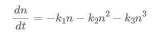

Figure 2. (a) Possible charge behavior in the corresponding time scale after light excitation [14]. (b) Hot carrier thermalization and cooling after photoexcitation. (c) Charge recombination dynamics, including radiation recombination, defect assisted recombination, and direct and indirect auger recombination [27].
In the equation, k1, k2, and k3 are the rate constants associated with the defect auxiliary (single particle), radiative (two-particle), and Auger (three-particle) recombination processes, respectively, and n is the density of photogenerated carriers. Defect-assisted recombination is dependent on the energy depth and density of the defect, whereas the Auger recombination mainly takes place in perovskite absorbers with high carrier concentrations [29][30][31][32][33]. At the interface, minimizing defects and surface states is expected to reduce SRH recombination [34], and a larger Schottky barrier selectively extracts majority carriers and blocks minority carriers [35][36].
After charge dissociation and transfer, charge extraction occurs rapidly on a picosecond timescale. Charge extraction (injection) has a direct relationship with the incident photon-to-current conversion efficiency (IPCE) as well as Jsc. IPCE is defined as IPCE =ηLHE×ηinj×ηcc, where ηLHE is the light capture efficiency, ηinj is the electron injection yield, and ηcc is the charge collection efficiency [37]. As discussed above, the extraction efficiency of the interface charge is primarily decided by the ELA, which relies on the location of the adjacent interface materials. Good energy level alignment can produce an appropriate built-in potential, which is beneficial for charge transfer. In general, it is believed that an energy shift of approximately 0.2 eV is required in order to ensure resultful charge extraction on the ETL/perovskite and perovskite/HTL interface [29].
Charge extraction and ion migration defects are the main causes of charge accumulation, which occurs on a time scale exceeding one second. The accumulation of charge affects electrode polarization, interface energy level mismatch, built-in electric fields, as well as back charge transfer that is near the interface [13][38]. In addition, it has been shown that the main source of J-V hysteresis is caused by the accumulation of interface charges from the interfacial defects and ions, rather than by ion migration in the perovskite thin film during the charge-discharge 169 dynamics [39][40]. After being extracted, the charges need to be collected by the electrode within a few microseconds [41]. The charge transfer efficiencies at the working electrode/ETL interface and HTL/counter electrode interface, as well as the electrode material conductivity, mainly determine the charge collection. If the base electrode is made of FTO or ITO, and the top electrode of the CTL is made of metal Au or Ag, then the efficiency of charge collecting is generally high [42].
As discussed above, charges need to be transferred through multiple layers and through two interfaces (the charge extraction and collection interfaces), which can be seen as a series circuit. From this, the overall internal quantum efficiency (IQE) of the PSCs could be deduced as IQE = , where is the charge extraction efficiency, and is the charge collection efficiency. These are determined by interface charge-carrier dynamics. To achieve a high IQE, it is necessary to have a high charge extraction as well as a low recombination rate, which in turn needs suitable interface energy structures, charge distribution, and atomic bonding [14]. Therefore, charge carrier dynamics are crucial to device performance.
3. The Formation Causes and Characterization Methods of Interface Defects
The high defect densities in the carrier transport layer (CTL) and the perovskite layer capture carriers, leading to interfacial non-radiative recombination, resulting in a decrease in PCE and stability. Currently, many studies pay attention to the top surface of the perovskite layer [43][44] because it is difficult to expose the buried interface and characterize it accurately [45]. However, the accumulation of defects is more concentrated at the buried interface than at the top interface, making the study of buried interface defects more important [46]. The delamination process proposed by Zhu et al. [47] (Figure 3a) can reveal the buried interface at the perovskite thin film. Macroscopically, combining the interface and surface characterization reveals that the losses at the buried interface are caused by sub-micron defects and inhomogeneities. SEM images show that there are more and larger lead halide plate-like particles at the bottom than at the top (Figure 3b), and further analysis using nanoscale Fourier-transform infrared spectroscopy (nano-FTIR) and PL reveal that the lateral concentration inhomogeneity of the main organic cations is more pronounced at the bottom than at the top (Figure 3c). Sub-micron defects and inhomogeneities are involved in the non-radiative recombination center, limiting the performance of the device.
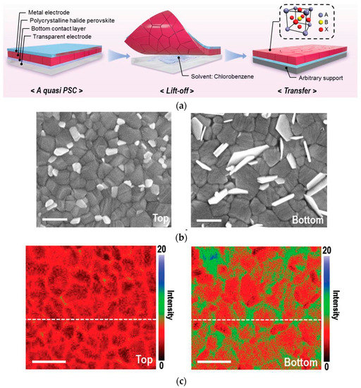
Figure 3. (a) Stripping exposes the buried interface. (b) SEM images of upper and lower surfaces of perovskite films. (c) Nano-FTIR images of upper and lower surfaces of perovskite films [47].
From a microscopic perspective, in an ideal semiconductor crystal structure, every atom is in the right position, with no defects or impurities (Figure 4a). However, due to the solution deposition method used to prepare perovskite thin films and the subsequent rapid crystallization annealing process, a large number of unavoidable defects exist in the actual prepared semiconductor. Figure 4a shows three types of point defects (vacancies, interstitials, and antisites) [48][49], which can be intrinsic or introduced by foreign atoms. In addition to point defects, Figure 4a shows two types of defect pairs (Frenkel and Schottky defects) [50]. The point defects and defect pairs consist of a range of dimensional defects, as shown in Figure 4a, such as 1D defect dislocations formed along the crystal, 2D defects formed at the grain surfaces and boundaries, and 3D defects that may lead to volume changes in the crystal. The 3D defect contains precipitates (tiny volumes with various crystal structures), second phase domains, and large voids [51][52].
Currently, first-principles calculations are commonly used to calculate the theoretical formation energy of point defects [53][54]. Yin et al. [55] theoretically calculated the energy level positions of point defects within MAPbI3, as shown in Figure 4b. Among them, most of the point defects in MAPbI3 are shallow-level defects, where the difference between the ground-state energy level of the defect and the migration edge of the valence band or conduction band is equal to or less than the thermal excitation energy kBT at room temperature [56]. Only IMA, IPb, PbI, and Pbi are deep-level defects within the perovskite bandgap, where the energy difference is larger than kBT [57]. Deep-level defects can capture electrons or holes, which are unable to escape by thermal activation and are eliminated by carrier recombination of opposite charges. This is the main factor for non-radiative recombination [58]. Therefore, defects in polycrystalline perovskite thin film bulk have little effect on non-radiative recombination [56].
Special attention has been paid to defects in the thin film interface. Xiao et al. demonstrated the existence of a high-density trap near the surface or a grain boundary of perovskite film through photoluminescence (PL) and thermal admittance spectroscopy (TAS) [59]. Currently, common interface defects include cation vacancies, anion vacancies, and anti-site defects, as illustrated in Figure 5c [60]. Wang et al. [61] used density functional theory (DFT) to calculate the formation energies of four types of defects on the surface of perovskite thin films and compared the formation energies of these defects on the surface and inside the films. The PbI antisite defect is easy to form on the surface of perovskite thin films and is dominant. As a deep-level defect, the PbI antisite defect causes serious non-radiative recombination in the device. The results indicate that the charge trap density is 1–2 orders of magnitude higher at the interface of polycrystalline perovskite [46]. For buried interfaces studied, they generally refer to the interface in the middle of the electron transport layer and the perovskite layer, which contains abundant oxygen vacancies, hydroxyl groups, and unsaturated coordinated metal atoms [62][63]. Thus, defects on the surface of perovskite and the interface of PSCs are critical to the performance of the device.
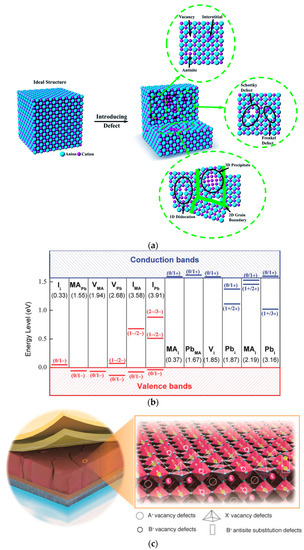
Figure 5. (a) Ideal and defective crystal structures [51]. (b) Calculation of transition energy levels for CH3NH3PbI3 (MA) midpoint defects. Recipient/donor is shown in terms of formation energy (left to right) and neutral defect formation energy is shown in parentheses [55]. (c) Possible surface defects on perovskite crystals (interstitials, substitutional, and vacancies) [60].
Research on defect characterization techniques is required to characterize defects or defect density and energy levels. Measurement techniques such as space charge limited current (SCLC), thermally stimulated current (TSC), thermal admittance spectroscopy (TAS), steady-state photoluminescence (SSPL), and deep level transient spectroscopy (DLTS) are used for this purpose. The SCLC is often used to measure material properties such as defect density, conductivity, carrier density, and mobility [64][65][66][67]. Although SCLC has been widely accepted for evaluating defect density in MTP, there are also some drawbacks. First of all, the SCLC can only show the density of one type of charge defect (electron trap or hole trap) at one time by means of one charge-type device. In addition, the VTFL estimation of defect density assumes that the linear part of J-V is always present in the ohmic region until the defect is fully filled, as shown in Figure 5a [64]. However, it is also possible that the starting point is due to the field ionization of the defect or the start of the double injection effect. Therefore, there is a possibility of incorrect assumptions of the estimated defect density [68].
TAS measures defect density by tracking the capacitance change of the defect during the alternating current (AC) voltage, including deep-level defects and shallow-level defects [69][70][71][72]. In typical PSCs, capacitance is mainly due to the discharge of charges trapped in defects under AC frequency variation. The semiconductor defect density is related to the position of the Fermi level, as shown in Figure 5b [72]. TAS is one of the most efficient methods for qualitatively comparing defect density in perovskite thin films under different conditions.
However, it is only the defect traps that are lower than the energy threshold that can capture or emit electric charges and produce capacitive signals. Additionally, capture charges that are temperature-dependent and have long thermal emission times cannot lead to capacitance signals. These factors reduce the accuracy of measuring the defect density [69]. The fundamental principle of the TSC is that it is possible to partially fill the defect trap with an optically excited electron at very low temperatures. These electrons can be thermally excited to the CBM through dark heating, producing a current signal ITSC [73]. The relationship between TSC and temperature for different devices is shown in Figure 5c [74]. However, TSC is only able to estimate the lower limit of defect density in MTP. Inaccuracies in estimation may occur due to incomplete defect filling, charge recombination, and other processes.
DLTS is used to detect deep-level defects [75]. In DLTS tests, different voltage signals are applied at different temperatures to measure changes in capacitance, current (i-DLTS), or charge (Q-DLTS) over time. First, most of the mobile charge carriers are depleted by reverse-biasing the semiconductor junction. Then, the voltage is zeroed briefly by a positive voltage pulse, and the empty trap is filled. At the end of the pulse, the semiconductor junction is reverse-biased again. In this case, the movement of the charge causes a change in the transient capacitance. The defect state and the energy difference of the band edge are determined by using the variation of the defect emission rate versus temperature and the defect capture cross section. Figure 5d shows DLTS spectra of perovskite films before and after I3− passivation [76]. For instance, it could miss some charge trapped in defects that are not filled under forward bias. Additionally, if the emission rate of the thermal is quite larger than that of optical emission, then the transient disappears as the defects are no longer filled between pulses. This shows that the DLTS is not capable of detecting shallow defects with high thermal emission rates.
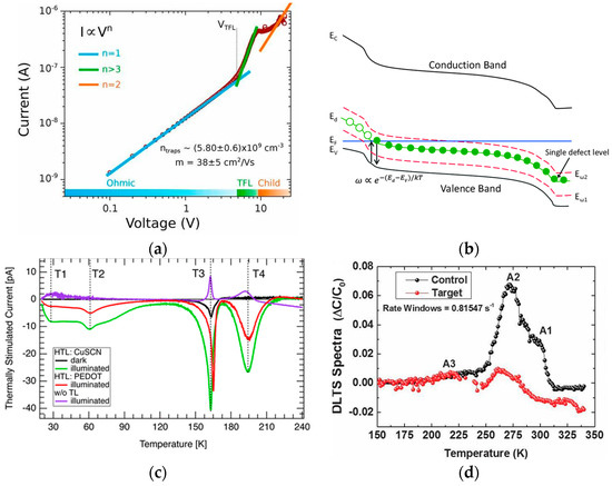
Figure 5. (a) SCLC curve of perovskite devices [64]. (b) A schematic band diagram of p-type semiconductor junction with a single trap level Ed and two measurement energies,Eω1 and Eω2 [72]. (c) TSC plot with a CuSCN HTL (green), a PEDOT: PSS HTL (red), no transport layer (purple), and reference measurement (black), with TSC peaks (T1–T4) represented by dashed lines [74]. (d) DLTS spectra of the control and target layers measured [76].
In order to make up for the shortcomings of different characterization methods, characterization techniques are often combined. Meggiolaro et al. [77] utilized first-principle calculations (DFT) and high-sensitivity photoluminescence and transient absorption measurements to determine the origin of defects. Stecker et al. [78] explored the surface defect properties and a few defect types (at atomic scale) by combining DFT calculation with STM [79]. There are also some indirect methods. Yang et al. [80] used the Lewis acid passivation effect to distinguish between halide defects and Pb defects, with the former being more pronounced. The existence of trap states on the surface of Pb0 was determined by Zu et al., using XPS and UPS [81]. Although there have been many successful cases, it is still very difficult to accurately identify and quantitatively detect defects.
This entry is adapted from the peer-reviewed paper 10.3390/en16135015
References
- Jeon, N.J.; Noh, J.H.; Yang, W.S.; Kim, Y.C.; Ryu, S.; Seo, J.; Seok, S.I. Compositional engineering of perovskite materials for high-performance solar cells. Nature 2015, 517, 476–480.
- Wehrenfennig, C.; Eperon, G.E.; Johnston, M.B.; Snaith, H.J.; Herz, L.M. High charge carrier mobilities and lifetimes in organolead trihalide perovskites. Adv. Mater. 2014, 26, 1584–1589.
- Xiao, Z.; Dong, Q.; Bi, C.; Shao, Y.; Yuan, Y.; Huang, J. Solvent annealing of perovskite-induced crystal growth for photovoltaic-device efficiency enhancement. Adv. Mater. 2014, 26, 6503–6509.
- Miyata, A.; Mitioglu, A.; Plochocka, P.; Portugall, O.; Wang, J.T.-W.; Stranks, S.D.; Snaith, H.J.; Nicholas, R.J. Direct measurement of the exciton binding energy and effective masses for charge carriers in organic–inorganic tri-halide perovskites. Nat. Phys. 2015, 11, 582–587.
- Kojima, A.; Teshima, K.; Shirai, Y.; Miyasaka, T. Organometal Halide Perovskites as Visible-Light Sensitizers for Photovoltaic Cells. J. Am. Chem. Soc. 2009, 131, 6050.
- NREL Best Research-Cell Efficiencies. Available online: https://www.nrel.gov/pv/assets/pdfs/best-research-cell-efficiencies-rev220630.pdf (accessed on 20 October 2022).
- Isikgor, F.H.; Zhumagali, S.; Merino, L.V.T.; De Bastiani, M.; McCulloch, I.; De Wolf, S. Molecular engineering of contact interfaces for high-performance perovskite solar cells. Nat. Rev. Mater. 2022, 8, 89–108.
- Correa-Baena, J.-P.; Saliba, M.; Buonassisi, T.; Gratzel, M.; Abate, A.; Tress, W.; Hagfeldt, A. Promises and challenges of perovskite solar cells. Science 2017, 358, 739–744.
- Park, N.-G.; Segawa, H. Research Direction toward Theoretical Efficiency in Perovskite Solar Cells. ACS Photonics 2018, 5, 2970–2977.
- Xiang, W.; Liu, S.F.; Tress, W. Interfaces and Interfacial Layers in Inorganic Perovskite Solar Cells. Angew. Chem. Int. Ed. Engl. 2021, 60, 26440–26453.
- Luo, D.; Li, X.; Dumont, A.; Yu, H.; Lu, Z.H. Recent Progress on Perovskite Surfaces and Interfaces in Optoelectronic Devices. Adv. Mater. 2021, 33, e2006004.
- Chen, H.; Chen, Y.; Zhang, T.; Liu, X.; Wang, X.; Zhao, Y. Advances to High-Performance Black-Phase FAPbI3 Perovskite for Efficient and Stable Photovoltaics. Small Struct. 2021, 2, 2000130.
- Yang, Z.; Dou, J.; Wang, M. Interface Engineering in n-i-p Metal Halide Perovskite Solar Cells. Sol. RRL 2018, 2, 1800177.
- Shi, J.; Li, Y.; Li, Y.; Li, D.; Luo, Y.; Wu, H.; Meng, Q. From Ultrafast to Ultraslow: Charge-Carrier Dynamics of Perovskite Solar Cells. Joule 2018, 2, 879–901.
- Ponseca, C.S.J.; Savenije, T.J.; Abdellah, M.; Zheng, K.; Yartsev, A.; Pascher, T.; Harlang, T.; Chabera, P.; Pullerits, T.; Stepanov, A.; et al. Organometal halide perovskite solar cell materials rationalized: Ultrafast charge generation, high and microsecond-long balanced mobilities, and slow recombination. J. Am. Chem. Soc. 2014, 136, 5189–5192.
- Sum, T.C.; Mathews, N.; Xing, G.; Lim, S.S.; Chong, W.K.; Giovanni, D.; Dewi, H.A. Spectral Features and Charge Dynamics of Lead Halide Perovskites: Origins and Interpretations. Acc. Chem. Res. 2016, 49, 294–302.
- Frenkel, J. On the Transformation of Light into Heat in Solids. II. Phys. Rev. 1931, 37, 1276–1294.
- Wannier, G.H. The Structure of Electronic Excitation Levels in Insulating Crystals. Phys. Rev. 1937, 52, 191–197.
- Elliott, R.J. Intensity of Optical Absorption by Excitons. Phys. Rev. 1957, 108, 1384–1389.
- Fang, H.; Li, X.; Zhou, Y.; Sun, H. Ultrafast Spectroscopy of Hot Carriers in Perovskites. Acta Opt. Sin. 2021, 41, 0823009.
- Shockley, W.; Queisser, H.J. Detailed Balance Limit of Efficiency of p-n Junction Solar Cells. J. Appl. Phys. 1961, 32, 510–519.
- Xing, G.; Mathews, N.; Sun, S.; Lim, S.S.; Lam, Y.M.; Graetzel, M.; Mhaisalkar, S.; Sum, T.C. Long-Range Balanced Electron- and Hole-Transport Lengths in Organic-Inorganic CH3NH3PbI3. Science 2013, 342, 344–347.
- Stranks, S.D.; Eperon, G.E.; Grancini, G.; Menelaou, C.; Alcocer, M.J.P.; Leijtens, T.; Herz, L.M.; Petrozza, A.; Snaith, H.J. Electron-Hole Diffusion Lengths Exceeding 1 Micrometer in an Organometal Trihalide Perovskite Absorber. Science 2013, 342, 341–344.
- Hegedus, S.; Luque, A. Handbook of Photovoltaic Science and Engineering; John Wiley & Sons: Hoboken, NJ, USA, 2011.
- Sze, S.M.; Li, Y.; Ng, K.K. Physics of Semiconductor Devices; John Wiley & Sons: Hoboken, NJ, USA, 2021.
- Chen, J.; Park, N.G. Causes and Solutions of Recombination in Perovskite Solar Cells. Adv. Mater. 2019, 31, e1803019.
- Luo, D.; Su, R.; Zhang, W.; Gong, Q.; Zhu, R. Minimizing non-radiative recombination losses in perovskite solar cells. Nat. Rev. Mater. 2019, 5, 44–60.
- Ball, J.M.; Petrozza, A. Defects in perovskite-halides and their effects in solar cells. Nat. Energy 2016, 1, 16149.
- Huang, J.; Yuan, Y.; Shao, Y.; Yan, Y. Understanding the physical properties of hybrid perovskites for photovoltaic applications. Nat. Rev. Mater. 2017, 2, 17042.
- Aranda, C.; Guerrero, A.; Bisquert, J. Ionic Effect Enhances Light Emission and the Photovoltage of Methylammonium Lead Bromide Perovskite Solar Cells by Reduced Surface Recombination. ACS Energy Lett. 2019, 4, 741–746.
- Yang, D.; Zhang, X.; Wang, K.; Wu, C.; Yang, R.; Hou, Y.; Jiang, Y.; Liu, S.; Priya, S. Stable Efficiency Exceeding 20.6% for Inverted Perovskite Solar Cells through Polymer-Optimized PCBM Electron-Transport Layers. Nano Lett. 2019, 19, 3313–3320.
- Abdi-Jalebi, M.; Dar, M.I.; Senanayak, S.P.; Sadhanala, A.; Andaji-Garmaroudi, Z.; Pazos-Outon, L.M.; Richter, J.M.; Pearson, A.J.; Sirringhaus, H.; Graetzel, M.; et al. Charge extraction via graded doping of hole transport layers gives highly luminescent and stable metal halide perovskite devices. Sci. Adv. 2019, 5, eaav2012.
- Arora, N.; Dar, M.I.; Hinderhofer, A.; Pellet, N.; Schreiber, F.; Zakeeruddin, S.M.; Graetzel, M. Perovskite solar cells with CuSCN hole extraction layers yield stabilized efficiencies greater than 20%. Science 2017, 358, 768–771.
- Wang, S.; Zhu, Y.; Sun, W.; Miao, X.; Ma, Z.; Yang, C.; Liu, B.; Li, S.; Ma, R.; Wang, C. Large guanidinium cation enhance photovoltage for perovskite solar cells via solution-processed secondary growth technique. Sol. Energy 2018, 176, 118–125.
- Tress, W.; Yavari, M.; Domanski, K.; Yadav, P.; Niesen, B.; Correa Baena, J.P.; Hagfeldt, A.; Graetzel, M. Interpretation and evolution of open-circuit voltage, recombination, ideality factor and subgap defect states during reversible light-soaking and irreversible degradation of perovskite solar cells. Energy Environ. Sci. 2018, 11, 151–165.
- Wolff, C.M.; Zu, F.; Paulke, A.; Toro, L.P.; Koch, N.; Neher, D. Reduced Interface-Mediated Recombination for High Open-Circuit Voltages in CH3NH3PbI3 Solar Cells. Adv. Mater. 2017, 29, 1700159.
- Chen, J.; Sheng, Y.; Ko, S.; Liu, L.; Han, H.; Li, X. Push–pull porphyrins with different anchoring group orientations for fully printable monolithic dye-sensitized solar cells with mesoscopic carbon counter electrodes. New J. Chem. 2015, 39, 5231–5239.
- Rajagopal, A.; Yao, K.; Jen, A.K. Toward Perovskite Solar Cell Commercialization: A Perspective and Research Roadmap Based on Interfacial Engineering. Adv. Mater. 2018, 30, e1800455.
- Wang, H.; Guerrero, A.; Bou, A.; Al-Mayouf, A.M.; Bisquert, J. Kinetic and material properties of interfaces governing slow response and long timescale phenomena in perovskite solar cells. Energy Environ. Sci. 2019, 12, 2054–2079.
- Weber, S.A.L.; Hermes, I.M.; Turren-Cruz, S.-H.; Gort, C.; Bergmann, V.W.; Gilson, L.; Hagfeldt, A.; Graetzel, M.; Tress, W.; Berger, R. How the formation of interfacial charge causes hysteresis in perovskite solar cells. Energy Environ. Sci. 2018, 11, 2404–2413.
- Shi, J.; Li, D.; Luo, Y.; Wu, H.; Meng, Q. Opto-electro-modulated transient photovoltage and photocurrent system for investigation of charge transport and recombination in solar cells. Rev. Sci. Instrum. 2016, 87, 123107.
- Yoo, J.J.; Wieghold, S.; Sponseller, M.C.; Chua, M.R.; Bertram, S.N.; Hartono, N.T.P.; Tresback, J.S.; Hansen, E.C.; Correa-Baena, J.-P.; Bulović, V.; et al. An interface stabilized perovskite solar cell with high stabilized efficiency and low voltage loss. Energy Environ. Sci. 2019, 12, 2192–2199.
- Jiang, Q.; Zhao, Y.; Zhang, X.; Yang, X.; Chen, Y.; Chu, Z.; Ye, Q.; Li, X.; Yin, Z.; You, J. Surface passivation of perovskite film for efficient solar cells. Nat. Photonics 2019, 13, 460–466.
- Jung, E.H.; Jeon, N.J.; Park, E.Y.; Moon, C.S.; Shin, T.J.; Yang, T.Y.; Noh, J.H.; Seo, J. Efficient, stable and scalable perovskite solar cells using poly(3-hexylthiophene). Nature 2019, 567, 511–515.
- Deng, J.; Zhang, H.; Wei, K.; Xiao, Y.; Zhang, C.; Yang, L.; Zhang, X.; Wu, D.; Yang, Y.; Zhang, J. Molecular Bridge Assisted Bifacial Defect Healing Enables Low Energy Loss for Efficient and Stable Perovskite Solar Cells. Adv. Funct. Mater. 2022, 32, 2209516.
- Ni, Z.; Bao, C.; Liu, Y.; Jiang, Q.; Wu, W.-Q.; Chen, S.; Dai, X.; Chen, B.; Hartweg, B.; Yu, Z.; et al. Resolving spatial and energetic distributions of trap states in metal halide perovskite solar cells. Science 2020, 367, 1352–1358.
- Yang, X.; Luo, D.; Xiang, Y.; Zhao, L.; Anaya, M.; Shen, Y.; Wu, J.; Yang, W.; Chiang, Y.H.; Tu, Y.; et al. Buried Interfaces in Halide Perovskite Photovoltaics. Adv. Mater. 2021, 33, e2006435.
- Liu, N.; Yam, C. First-principles study of intrinsic defects in formamidinium lead triiodide perovskite solar cell absorbers. Phys. Chem. Chem. Phys. 2018, 20, 6800–6804.
- Yin, W.-J.; Shi, T.; Yan, Y. Unusual defect physics in CH3NH3PbI3 perovskite solar cell absorber. Appl. Phys. Lett. 2014, 104, 063903.
- Kim, J.; Lee, S.H.; Lee, J.H.; Hong, K.H. The Role of Intrinsic Defects in Methylammonium Lead Iodide Perovskite. J. Phys. Chem. Lett. 2014, 5, 1312–1317.
- Ran, C.; Xu, J.; Gao, W.; Huang, C.; Dou, S. Defects in metal triiodide perovskite materials towards high-performance solar cells: Origin, impact, characterization, and engineering. Chem. Soc. Rev. 2018, 47, 4581–4610.
- Ono, L.K.; Liu, S.F.; Qi, Y. Reducing Detrimental Defects for High-Performance Metal Halide Perovskite Solar Cells. Angew. Chem. Int. Ed. Engl. 2020, 59, 6676–6698.
- Du, M.H. Density Functional Calculations of Native Defects in CH3NH3PbI3: Effects of Spin-Orbit Coupling and Self-Interaction Error. J. Phys. Chem. Lett. 2015, 6, 1461–1466.
- Zakutayev, A.; Caskey, C.M.; Fioretti, A.N.; Ginley, D.S.; Vidal, J.; Stevanovic, V.; Tea, E.; Lany, S. Defect Tolerant Semiconductors for Solar Energy Conversion. J. Phys. Chem. Lett. 2014, 5, 1117–1125.
- Yin, W.J.; Shi, T.; Yan, Y. Unique properties of halide perovskites as possible origins of the superior solar cell performance. Adv. Mater. 2014, 26, 4653–4658.
- Li, W.; Liu, J.; Bai, F.-Q.; Zhang, H.-X.; Prezhdo, O.V. Hole Trapping by Iodine Interstitial Defects Decreases Free Carrier Losses in Perovskite Solar Cells: A Time-Domain Ab Initio Study. ACS Energy Lett. 2017, 2, 1270–1278.
- Xiao, Z.; Yuan, Y.; Wang, Q.; Shao, Y.; Bai, Y.; Deng, Y.; Dong, Q.; Hu, M.; Bi, C.; Huang, J. Thin-film semiconductor perspective of organometal trihalide perovskite materials for high-efficiency solar cells. Mater. Sci. Eng. R Rep. 2016, 101, 1–38.
- Saliba, M.; Matsui, T.; Seo, J.Y.; Domanski, K.; Correa-Baena, J.P.; Nazeeruddin, M.K.; Zakeeruddin, S.M.; Tress, W.; Abate, A.; Hagfeldt, A.; et al. Cesium-containing triple cation perovskite solar cells: Improved stability, reproducibility and high efficiency. Energy Environ. Sci. 2016, 9, 1989–1997.
- Xiao, Z.; Yuan, Y.; Shao, Y.; Wang, Q.; Dong, Q.; Bi, C.; Sharma, P.; Gruverman, A.; Huang, J. Giant switchable photovoltaic effect in organometal trihalide perovskite devices. Nat. Mater. 2015, 14, 193–198.
- Aydin, E.; De Bastiani, M.; De Wolf, S. Defect and Contact Passivation for Perovskite Solar Cells. Adv. Mater. 2019, 31, e1900428.
- Wang, R.; Xue, J.; Wang, K.-L.; Wang, Z.-K.; Luo, Y.; Fenning, D.; Xu, G.; Nuryyeva, S.; Huang, T.; Zhao, Y.; et al. Constructive molecular configurations for surface-defect passivation of perovskite photovoltaics. Science 2019, 366, 1509–1513.
- Zhang, P.; Wu, J.; Zhang, T.; Wang, Y.; Liu, D.; Chen, H.; Ji, L.; Liu, C.; Ahmad, W.; Chen, Z.D.; et al. Perovskite Solar Cells with ZnO Electron-Transporting Materials. Adv. Mater. 2018, 30, 1703737.
- Dai, Z.; Yadavalli, S.K.; Chen, M.; Abbaspourtamijani, A.; Qi, Y.; Padture, N.P. Interfacial toughening with self-assembled monolayers enhances perovskite solar cell reliability. Science 2021, 372, 618–622.
- Shi, D.; Adinolfi, V.; Comin, R.; Yuan, M.; Alarousu, E.; Buin, A.; Chen, Y.; Hoogland, S.; Rothenberger, A.; Katsiev, K.; et al. Low trap-state density and long carrier diffusion in organolead trihalide perovskite single crystals. Science 2015, 347, 519–522.
- Cai, F.; Yang, L.; Yan, Y.; Zhang, J.; Qin, F.; Liu, D.; Cheng, Y.-B.; Zhou, Y.; Wang, T. Eliminated hysteresis and stabilized power output over 20% in planar heterojunction perovskite solar cells by compositional and surface modifications to the low-temperature-processed TiO2 layer. J. Mater. Chem. A 2017, 5, 9402–9411.
- Liu, Z.; Hu, J.; Jiao, H.; Li, L.; Zheng, G.; Chen, Y.; Huang, Y.; Zhang, Q.; Shen, C.; Chen, Q.; et al. Chemical Reduction of Intrinsic Defects in Thicker Heterojunction Planar Perovskite Solar Cells. Adv. Mater. 2017, 29, 1606774.
- Son, D.Y.; Kim, S.G.; Seo, J.Y.; Lee, S.H.; Shin, H.; Lee, D.; Park, N.G. Universal Approach toward Hysteresis-Free Perovskite Solar Cell via Defect Engineering. J. Am. Chem. Soc. 2018, 140, 1358–1364.
- Bube, R.H. Trap Density Determination by Space-Charge-Limited Currents. J. Appl. Phys. 1962, 33, 1733–1737.
- Walter, T.; Herberholz, R.; Müller, C.; Schock, H.W. Determination of defect distributions from admittance measurements and application to Cu(In,Ga)Se2 based heterojunctions. J. Appl. Phys. 1996, 80, 4411–4420.
- Wang, Q.; Shao, Y.; Dong, Q.; Xiao, Z.; Yuan, Y.; Huang, J. Large fill-factor bilayer iodine perovskite solar cells fabricated by a low-temperature solution-process. Energy Environ. Sci. 2014, 7, 2359–2365.
- Lee, J.-W.; Kim, D.-H.; Kim, H.-S.; Seo, S.-W.; Cho, S.M.; Park, N.-G. Formamidinium and Cesium Hybridization for Photo- and Moisture-Stable Perovskite Solar Cell. Adv. Energy Mater. 2015, 5, 1501310.
- Duan, H.S.; Zhou, H.; Chen, Q.; Sun, P.; Luo, S.; Song, T.B.; Bob, B.; Yang, Y. The identification and characterization of defect states in hybrid organic-inorganic perovskite photovoltaics. Phys. Chem. Chem. Phys. 2015, 17, 112–116.
- Haering, R.R.; Adams, E.N. Theory and application of thermally stimulated currents in photoconductors. Phys. Rev. 1960, 117, 451–454.
- Baumann, A.; Vath, S.; Rieder, P.; Heiber, M.C.; Tvingstedt, K.; Dyakonov, V. Identification of Trap States in Perovskite Solar Cells. J. Phys. Chem. Lett. 2015, 6, 2350–2354.
- Rosenberg, J.W.; Legodi, M.J.; Rakita, Y.; Cahen, D.; Diale, M. Laplace current deep level transient spectroscopy measurements of defect states in methylammonium lead bromide single crystals. J. Appl. Phys. 2017, 122, 145701.
- Yang, W.S.; Park, B.-W.; Jung, E.H.; Jeon, N.J.; Kim, Y.C.; Lee, D.U.; Shin, S.S.; Seo, J.; Kim, E.K.; Noh, J.H.; et al. Iodide management in formamidinium-lead-halide-based perovskite layers for efficient solar cells. Science 2017, 356, 1376–1379.
- Martiradonna, L. Riddles in perovskite research. Nat. Mater. 2018, 17, 377.
- Meggiolaro, D.; Motti, S.G.; Mosconi, E.; Barker, A.J.; Ball, J.; Andrea Riccardo Perini, C.; Deschler, F.; Petrozza, A.; De Angelis, F. Iodine chemistry determines the defect tolerance of lead-halide perovskites. Energy Environ. Sci. 2018, 11, 702–713.
- Stecker, C.; Liu, K.; Hieulle, J.; Ohmann, R.; Liu, Z.; Ono, L.K.; Wang, G.; Qi, Y. Surface Defect Dynamics in Organic-Inorganic Hybrid Perovskites: From Mechanism to Interfacial Properties. ACS Nano 2019, 13, 12127–12136.
- Yang, Z.; Dou, J.; Kou, S.; Dang, J.; Ji, Y.; Yang, G.; Wu, W.Q.; Kuang, D.B.; Wang, M. Multifunctional Phosphorus-Containing Lewis Acid and Base Passivation Enabling Efficient and Moisture-Stable Perovskite Solar Cells. Adv. Funct. Mater. 2020, 30, 1910710.
- Zu, F.; Amsalem, P.; Ralaiarisoa, M.; Schultz, T.; Schlesinger, R.; Koch, N. Surface State Density Determines the Energy Level Alignment at Hybrid Perovskite/Electron Acceptors Interfaces. ACS Appl. Mater. Interfaces 2017, 9, 41546–41552.
This entry is offline, you can click here to edit this entry!