Your browser does not fully support modern features. Please upgrade for a smoother experience.
Please note this is a comparison between Version 1 by Ho SOON Soonmin and Version 2 by Sirius Huang.
Solar energy is free from noise and environmental pollution. It could be used to replace non-renewable sources such as fossil fuels, which are in limited supply and have negative environmental impacts. The first generation of solar cells was made from crystalline silicon. They were relatively efficient, however very expensive because they require a lot of energy to purify the silicon. The production of solar cells has been improved since the first generation (thin-film solar cells, dye-sensitized solar cells, perovskite solar cells, and organic solar cells).
- solar energy
- thin films
- organic solar cells
- crystalline silicon
- dye-sensitized solar cells
- power conversion efficiency
- renewable energy
- perovskite solar cell
1. Introduction
The process of the conversion of energy from the most abundant source, the sun, into electricity is termed as the photovoltaic effect [1]. Semiconductor materials are the basic requirement for the process of the conversion of photons into electrons [2]. These materials can be divided into organic and inorganic [3] substances.
Photovoltaic solar-cell technologies can be divided into three distinct generations [4]. The first generation was crystalline silicon. This technology currently dominates the global solar-cell market due to it has good performance and stability. The second generation is based on thin films of amorphous silicon and inorganic semiconductor elements such as copper indium gallium selenide (CIGS), cadmium telluride (CdTe), and copper indium selenide (CuInSe2). Moreover, the third generation is based on organic semiconductors. Organic solar cells can either be based on dye-sensitized solar cells [5], multiple junctions based on group IV and group III–V elements, and hybrid solar cells that contain inorganic quantum dots or nanomaterials with organic materials [6]. The potential of organic solar cells for practical applications [7] is demonstrated by recent enhancements in the power-conversion efficiency (PCE).
Organic–inorganic hybrid perovskites (OIHPs) are a group of materials which show magnificent potential for high performance and low production costs in photovoltaic technology [8]. Any material which has an identical crystal structure with calcium titanium oxide (CaTiO3) is recognized as a “perovskite” structure, as named by the Russian Mineralogist Lev Alek-sevich von Perrovski (1839). These perovskites have a stoichiometry of ABX3 three-dimensional structure, where the “A” and “B”-sites are occupied by larger and smaller cations, respectively, and the anion resides at the “X”-site. The 3D crystal structure of ABX3 consists of corner-shared BX6 octahedrals and “A” cations occupy the cavity between them [9][10][9,10]. Materials with perovskite structures are quite abundant in nature and can be found in an enormous number of compounds that show a wide range of physical properties, applications, and importance.
Perovskite solar cells can have a conventional (regular) or an inverted PSC structure, depending on the architecture. TiO2 and n-type semiconductors are used in the normal configuration, whereas p-type poly (3,4-ethylene dioxythiophene)-poly(styrene sulfonate) (PEDOT: PSS) are used in the inverted configuration. Typical mesoscopic perovskite solar cell structures consist of a glass surface with a transparent conducting oxide (TCO), such as in FTO (F:SnO2), in which an anode is deposited on the glass substrate, a dense (compact) layer of TiO2 is a hole-blocking layer, and a mesoporous layer of TiO2 serves as an electron-transporting layer (ETL). Moreover, a layer of the perovskite material is used for light absorption, followed by a hole-transporting layer, followed by metal contacts to complete the device’s structure. This type of solar cell has an organic material with a perovskite structure in its absorbing layer, most typically a lead–metal hybrid (Methylammonium lead iodide perovskite, MAPbI3). Methylammonium lead iodide is an ambipolar semiconductor that may transmit both electrons and holes to the collecting electrodes. Because of this, perovskite solar cells can operate without a hole or electron conductor. The Spiro-OMeTAD polymer composition is the HTL material most frequently utilized in perovskite solar cells.
Perovskite solar cells’ superior absorption capabilities and low exciton binding energy are two of their most notable features. Light absorption is the initial physical process in solar systems. When a photon activates an active material with an energy higher than its bandgap, an exciton (electron-hole pairs) is produced. Excitons must reach the contacts after being photogenerated in the perovskite to be retrieved. The charge-transport capabilities of the perovskite play a role in this process. Compared with conventional solar cells, perovskite serves as an absorber in thin-film solar cells to offer effective transport of excitons. The remarkable PCE of these perovskite solar cells is produced by the material’s outstanding charge-transport properties. They possess long charge-carrier diffusion lengths surpassing 5 m and the associated lifetimes of 1 s in both single-crystal and polycrystalline films. These diffusion lengths guarantee that the produced charge can be recovered even from thicker films that absorb the input light completely. However, the interfacial contacts with the charge extraction layer also have a role in the device’s ultimate quality. After absorption and charge transmission, the photovoltaic process requires the extraction of the photogenerated charge. As a result, the optimal extraction interface should provide the least possible voltage, current, and FF loss. An optimal selective contact should not absorb light to prevent the reduction of light intensity in the perovskite. Similarly, there should not be any energetic losses during the absorber injection (no interfacial recombination). These contact materials need to be selective to enable one kind of carrier to be injected, but they also need to lower series resistance.
One of two major processes can result in charge separation in perovskite. One involves injecting photogenerated electrons into an n-type semiconductor such as TiO2, while the other involves injecting holes into a p-type material that transports holes, such as spiro-OMeTAD. To stop holes from reaching the TCO substrate (anode) and short-circuiting the cell, a hole-blocking layer is utilized between the TCO-conducting substrate and the mesoscopic scaffold and/or perovskite layer. On the other hand, using a mesoporous TiO2 layer greatly lessens the hysteresis behavior of PSC even if a hybrid organic–inorganic perovskite absorber can transfer photogenerated electrons to the conductive substrate itself.
Dye-sensitized solar cells (DSSC) were first discovered by professor Michael Gratzel in 1991. The DSSC consists of a working electrode [11], a counter electrode, and an electrolyte. Dyes (natural organic materials and synthetic materials) are attached to the TiO2 films, serve as the working electrodes. The DSSC consisting of ruthenium (II) polypyridyl complex (N3 dye) [12] showed a power-conversion efficiency of about 10%. A platinum conductive glass served as the counter electrode [11]. The working principle of DSSC converts sunlight into electricity through the creation of exciton. The semiconductor material is placed on a conductive transparent plate to form a thin layer. A dye monolayer layer is placed on the surface of the semiconductor. Photoexcitation experienced by the dye produces electrons excited from the valence band to the conduction band of the dye, which then enter the conduction band of the metal oxide. This electron injection is performed through the connection between titanium and the carboxyl group in the dye. This process produces a positively charged dye and a negatively charged TiO2 particle. The electrons then exit through the external circuit to the opposite electrode. This flow of electrons is used as electrical energy. The electron vacancies in the valence band of the dye are replaced by electrons from the electrolyte. The electrolyte used in DSSC is usually an organic solvent containing a redox system such as an iodide–triiodide pair. The regeneration of the sensitizer by iodide occurs by donating electrons in the valence band of the oxidized dye. The iodide is regenerated by reducing the triiodide at the opposite electrode by utilizing electrons from the external circuit. This process takes place continuously as a cycle so that a continuous current is produced.
Metal chalcogenide films are considered as important materials for solar-cell applications [13]. Several types of films (metal sulfide, metal selenide, and metal telluride) have been prepared using a vacuum method or non-vacuum deposition technique [14]. These films could be cheaper to produce, show good quality materials, and have the most potential for the future.
2. Organic Solar Cells
2.1. Advantages of Organic Solar Cells over Inorganic Solar Cells
The advantages of organic solar cells (OSC) over inorganic solar cells are threefold [15][16][15,16]. Firstly, in terms of the materials, limited silicon wafer technology leads to heavy, rigid, fragile, and bulky materials that are only available in a couple of colors. Conversely, the materials for OSC are light-weight, thin, flexible, and color-tunable, and can be customized to any design. Secondly, the fabrication process of inorganic solar cells is expensive, complicated, energy-intensive, must be conducted at high temperatures, and has limitations in the possible sizes of fabrications. On the other hand, OSC technology is cheap, simple, non-energy consuming, can be fabricated at ambient temperature, has no limitations in the size of fabrication, and has high speed production besides various possibilities of printing and coating fabrication techniques (such as inkjet, screen, and spray). Finally, the applications of inorganic solar cell are limited only to rooftops and open fields compared with the unlimited possibilities of OSC applications such as windows, screens, smart glasses, automotives, and the charging of mobile devices and laptops [17][18][19][17,18,19].2.2. Challenges for Organic Solar Cell Technology
Silicon is the most widely used material for the commercial photovoltaic market due to its high-power conversion efficiency [20][21][22][20,21,22]. Inorganic solar cells are associated with certain challenges such their its high-cost and complicated and energy-intensive fabrication protocols. Organic solar cells are gaining attention due to their simple fabrication protocols. OSC technology has not yet gained much attention commercially because of its low power-conversion efficiency (PCE) and limited lifetime [23][24][23,24]. The heterojunction generated by contact of donor and acceptor material is the basis of OSC. There are a number of challenges in OSC technology such as limited absorption efficiency of donor materials, hindered exciton diffusion, charge dissociation, and transport of charges. Different approaches to overcome these challenges could be improved in exciton diffusion length, crystal structure, and the collection of photogenerated carriers. These improvements can be realized by the application of polymer-based nanocomposites, plasmonics, and tandem architectures. Moreover, hybrid nanocomposites (composed of both organic and inorganic materials) can be a synergistic combination to take advantage of the unique properties of both components [25][26][27][25,26,27]. The operation of hybrid solar cells has more similarities with OSC. Hybrid solar cells are composed of n-type inorganic material along with p-type semiconductor polymer and are capable of achieving high PCE.2.3. Materials for Organic Solar Cells
Organic materials for OSC can be derivative of small molecules or semiconducting polymers [28]. Organic semiconductors have conjugated organic moieties such as dendrimers, pigments, dyes, polymers, and small molecules, which can be a good choice for OSC. Any OSC requires two types of materials: an electron pair donor and an electron pair acceptor. Conjugated polymers are employed as donor materials. Initially, poly(1,4-phenylenevinylene) (PPV) and its derivatives gained considerable attention due to their appropriate optoelectronic properties [29][30][29,30]. Later, polythiophene and its derivative, especially poly(3-hexylthiophene), P3HT, began to be used widely (as a donor material) owing to its stability, high carrier mobility, and solubility [31][32][33][31,32,33]. The structures of some important donor materials for OSC technology are listed in Figure 1. Although fullerene and its derivatives dominated OSC technology in the initial phase [34][35][36][37][38][34,35,36,37,38], small molecules such as 3,9-bis(2-methylene-(3-(1,1-dicyanomethylene)-indanone)-5,5,11,11-tetrakis(4hexylphenyl)-dithieno [2,3-d:2′,3′-d′]-s-indaceno [1,2-b:5,6-b′]dithiophene (ITIC), IHIC, and PCDTBT (termed as non-fullerene acceptors, NFA) have attracted considerable attention recently due to their superior properties [39][40][41][42][39,40,41,42]. Moreover, donor–acceptor conjugated polymers such as poly [2,6-(4,4-bis-(2-ethylhexyl)-4H-cyclopenta [2,1-b;3,4-b′]dithiophene)-alt-4,7(2,1,3-benzothiadiazole)], PCPDTBT [43], and poly [2,7-(9,9-dioctylcarbazole)-alt-4,7-bis(thiophen-2-yl)benzo-2,1,3-thiadiazole], PCzDTBT [44] have been employed. The structures of some important fullerene and non-fullerene acceptor materials are depicted in Figure 1.
Figure 1.
The structures of some important donor and acceptor materials of OSC.
The engineering of the input donor and acceptor materials can help in improving the optoelectronic properties of these materials, which, in turn, improve the performance of OSC. One of the major limitations of the donor materials for OSC is their limited capacity of absorbing the whole wavelength range of the solar spectrum. The absorption efficiency can be improved by increasing the HOMO level, decreasing the LUMO level, or by compressing the band gap between HOMO–LUMO levels [45][46][45,46]. Polymers have higher molar mass and possess longer conjugation lengths, and hence the energy band gap is lower [47][48][49][47,48,49]. Voltametric p-type doping can also help in improving the optoelectronic properties through broadening of the absorption spectrum [50][51][52][53][50,51,52,53]. Regioregularity of polymers facilitates the mobility of excitons and thus improve the performance of OSC [54][55][56][54,55,56]. Physiochemical properties of OSC materials can be easily tuned by changing their chemistry, which is a unique advantage compared with conventional inorganic solar cells. For instance, the introduction of flexible side-chains such as alkyl or alkoxy leads to an improvement of solubility while the introduction of electron-donating or -withdrawing substituents can help in the alignment of electronic energy levels. The improvement of the optoelectronic properties of polymers by chemical modifications is shown for several polymers such as poly(p-phenylene vinylene) [57] and P3HT [58][59][60][58,59,60]. Electron-withdrawing groups such as Fluorine on the polymer chain improve the charge transference by tuning of the LUMO level [61], while electron-donating substituents on the polymer chain enhance charge-carrier mobility by minimizing the structural defects due to an increase in the HOMO energy level [62][63][64][62,63,64].
Moreover, large donor–acceptor interfaces as provided by nanostructures render effective exciton dissociation and efficient charge transport [65][66][67][68][69][70][71][72][65,66,67,68,69,70,71,72]. Conjugated polymer-based metallic nanoparticles can be prepared by several methods [73][74][75][73,74,75]. Different metals can have peculiar and dissimilar effects on the optoelectronic properties of the nanocomposites and their performance in the context of solar cells [76][77][78][79][80][76,77,78,79,80]. The incorporation of silver (Ag) and gold (Au) nano particles in polymer bulk heterojunction solar cells enhances their performance owing to the improved absorption of sunlight. In the context of OSC, conjugated polymer nanowires are mostly used due to their ability to create percolation pathways for both electrons and holes, leading to higher device efficiency [81][82][83][84][81,82,83,84]. The applications of polymer nanowires have several advantages such as (a) better control over morphology, (b) appropriate matching of the exciton diffusion lengths to the widths and lengths of polymer nanowires, (c) large interfacial area between donor and acceptor, (d) existence of electrically bi-continuous morphology, (e) achievement of high absorption coefficient and high carrier mobilities, (f) possibility of manufacturing devices with high surface areas, and (g) the avoidance of blend phase-separation difficulties [85][86][85,86]. Thermal annealing of the P3HT/PCBM mixture at 120 °C for 60 min renders P3HT nanowires with improved crystallinity of P3HT and enhances the demixing between P3HT and PCBM [87].
3. Perovskite Solar Cells
3.1. The Meaning of Perovskite
Originally, the term “perovskite” referred to the calcium titanate crystal structure, which was identified in 1839 by German mineralogist Gustav Rose and given the name by Russian mineralogist Lev Perovski. Compounds with perovskite structures typically contain the formula ABX3, where ‘A’ and ‘B’ stand for cations and ‘X’ is an anion joining the two cations. These metal halide perovskites, consisting of lead (Pb2+), methyl-ammonium CH3NH3+, an organic cation, and a halide anion such as iodide (I) or bromide (Br), have drawn much attention as prospective perovskite solar-cell materials in recent years. Figure 25 displays three-dimensional (3D) and two-dimensional (2D) schematic designs as well as the usual unit cell arrangement of a perovskite compound. Usually, structures can be built from a wide variety of unique component combinations. By changing the composition of these substances, researchers may produce perovskite crystals with a variety of properties, including physical, optical, magnetic, and electrical.Figure 25.
(
a
) 3D and (
b
) 2D schematic diagrams and (
) the schematic diagram of a perovskite unit cell [116].
In 1958, Chr. Kn. Moller first discovered halide perovskites for cesium lead halides [89][117]. Following this, it was also observed that small organic molecules with effective radii less than 260 pm (such as MA (CH3NH3), FA (CH(NH)2)) could also accommodate the inside of the lead halide octahedrons from the analysis of Goldschimdt’s tolerance factor/octahedral factor; additionally, Dieter Weber, in 1978, successfully synthesized MAPbX3 (X = halogens (I, Br, Cl or Mixtures of them) and superhalogen (BF4, PF6)) for the first time [90][118]. Thereafter, researchers started working on layered 2D perovskite systems (commonly, (R-NH3)2MX4), where the extended inorganic lead halide octahedral cage is separated by large organo-ammonium cations [91][119]. The resurgent hybrid perovskite was initiated by the introduction of three-dimensional hybrid perovskites (CH3NH3PbI3 and CH3NH3PbBr3) as absorbers [92][120] in mesoporous solar cells by Miyasaka and co-workers in 2009. Since then, researchers across the globe have used them as absorber materials in photovoltaic cells and achieved PCE as high as 25.7% in sa ingle junction [93][121] and 29.8% in monolithic perovskite/Si tandem solar cells. Superior optoelectronic properties such as low bandgap with direct nature, high optical absorption both in visible and IR regions, ultrahigh diffusion length, high defect tolerance, large and balanced electron-hole mobilities, high photoluminescence quantum yield, and low surface recombination velocity make them attractive candidates for solar-cell application [94][95][122,123].
Nowadays, the various structures of perovskite solar cells such as mesoporous, planar, and inverted structures have been developed. In the mesoporous solar cells, the device structure was composed of glass/fluorine-doped tin oxide (FTO)/dense electron transport layer (ETL)/mesoporous oxide layer/perovskite layer (~500 nm)/hole transport layer (HTL)/metal electrode [96][97][98][124,125,126]. The mesoporous TiO2 is used as an ETL material allowing perovskites to penetrate into the pores to form an interconnected absorbing layer. Additionally, titanium dioxide (TiO2) also prevents the electron-hole recombination in the FTO by blocking the holes. Experimental results revealed that other oxide materials such as zinc oxide (ZnO), aluminum oxide (Al2O3), and zirconium dioxide (ZrO2) were also used as mesoporous oxide layers. In this structure, Spiro-OMeTAD (2,2′,7,7′-Tetrakis [N, N-di(4-methoxyphenyl) amino]-9,9′-spirobifluorene) is the most used HTL and noble metals such as Au, Ag, and Pt are used as the counter electrodes. In the case of planar structure, the mesoporous ETL is removed and only two sharp interfaces are observed between perovskites and two transport layers (ETL and HTL). As a result, the rapid and effective separation of electrons and holes are observed through the ETL and HTL, respectively [99][127]. Due to the minimum number of interfaces, planar heterojunction structures help to understand the operating mechanisms of light absorption and electron-hole separation precisely and optimize the structure for the development of highly efficient laminated perovskite photovoltaic cells. Besides the two abovementioned structures, perovskite solar cells without HTL have become an interesting research project due to their advantages of easy and simple device fabrication and high stability [100][128]. These perovskite materials served the purpose of both light absorbers and hole transport channels. Using device simulation, Minemoto and Murata showed that the built-in electric field was not affected if the work function of metal electrodes was close to the valence band maximum of the light-absorbing materials for the case of HTL-free perovskite solar cells [101][129].
Usually, the perovskite layer is spin-coated on the substrate via either a single-step or two-step process. In the single-step process, perovskite precursor (a mixture of CH3NH3I and PbI2 dissolved in DMF:DMSO) is spin-coated onto the FTO substrate in one step and kept at 1000 C to achieve a uniform perovskite film. In recent times, an anti-solvent method is effective, in which the perovskite precursor solution is prepared in the polar solvent and quenched during the process of spin coating by a non-polar solvent. It is often observed that precise control over the volume of quenching solvent and timing is very much essential to achieve uniform morphology and optimal device performance. In the two-step process, lead iodide (PbI2) was the first to be spin-coated and then transferred into a vessel where 1 molar CH3NH3I was dissolved in isopropanol. Other than these two frequently used methods, OIHPs can also be deposited via a ‘vacuum-assisted solution process’ (VASP) in which perovskite films are coated and annealed in a chamber filled with the organic component vapor [102][130].
3.2. Advantages and the Challenges of Perovskite Solar Cells
Perovskite photovoltaics have a high light-absorption coefficient (104 cm−1), which results in an impressive photocurrent generation [103][131], long carrier diffusion length, and solution processability [104][105][106][132,133,134]. Perovskite solar cells are cheaper to produce, owing to their inexpensive and naturally abundant materials (lead, iodine, carbon, and hydrogen) [107][135]. These solar cells show better defect tolerance than other solar semiconductors on the market [108][136], which increases their reusability and lowers production costs. Despite their benefits, the commercialization of perovskite solar cells is hampered by another factor. Water by itself (moisture) and other polar solvents provide a serious problem for perovskite solar cells. These solvents can alter the solvated phases of a perovskite and occasionally hydrate a perovskite to produce a monohydrate phase. Polar solvents can considerably be prevented from harming perovskite solar cells by modifying deposition techniques, according to reports. However, environmental moisture is unavoidable [109][137]. It is observed that various external factors such as oxygen, light, and heat have expedited the degradation, which can be slowed by choosing a proper composition of the perovskite material (such as FA0.85MA0.1Cs0.05PbI2.7Br0.3, which show better stability and power conversion efficiency) [110][111][112][113][138,139,140,141]. In addition, it was noted that the deposition of more hydrophobic and UV-stable ETL/HTL has improved the stability of the device (replacing TiO2 with SnO2). The combination of Ruddlesden–Popper (RP) 2D-layered perovskites with conventional 3D perovskites has improved the stability of the device as 2D perovskite passivate/encapsulate the device [114][142]. On the other hand, the use of an excessive amount of lead in the perovskite component is also another big challenge in its commercialization. As an alternative, tin-based perovskites are studied, but the PCE of such devices [115][143] is poor (PCE ~13%). Current-voltage hysteresis between the forward and reverse bias is another major issue. Although the reason for hysteresis is still under debate, it is commonly ascribed to the combination of ion migration with high levels of charge-carrier recombination. To achieve a truly low cost-per-watt and dominate the photovoltaic market, solar cells based on OIHPs should satisfy the much-heralded trio of high-power-conversion efficiency (PCE), yearlong lifetimes, and ultra-low manufacturing costs. Certainly, OIHP-based solar-cell devices are quite farther ahead than other thin-film technologies, as they have shown enormous potential for achieving this.4. Dye-Sensitized Solar Cells
Dye-sensitized solar cells (DSSC) are solar cells made of semiconductors that are coated with a dye to increase the efficiency of sunlight [116][147]. This type of solar cell was first introduced by Michael Gratzel. DSSCs are composed of a working electrode consisting of fluorine tin oxide (FTO) glass, titanium dioxide (TiO2), dye, an electrolyte consisting of an I¯/I3¯ redox pair, and a counter electrode consisting of platinum. DSSCs work in the visible region. DSSC components have undergone various developments over the years to increase their efficiency.4.1. Advantages and Limitations of Dye-Sensitized Solar Cells
Some of the advantages offered by dye-sensitized solar cells, including their relatively low cost of fabrication, operability under scattered light conditions, and the variable shape of the cell, which can be made opaque or opaque or optically transparent, thereby providing more value from an artistic point of view [117][148]. Organic solar cells have dyes derived from organic and synthetic organic materials. Examples of dyes from organic materials are mangosteen, juwet fruit, water henna, nail henna, blueberries, binahong leaves, carrots, kenikir, and mangosteen peel. Synthetic organic dyes such as ruthenium complex (N719) could produce a higher efficiency of 10.4–11.1% [118][119][149,150]. However, the cost of producing ruthenium complex dyes is still relatively high, thus encouraging the development of new dye sensitizers (complexes of osmium, rhenium, iron, and iridium) [120][151]. The advantages of using synthetic, organic dyes include their higher conversion efficiency (an efficiency increase of up to 30% in synthetic dyes, with organic dyes being 5%), increased chemical and thermal stability, the color being difficult to degrade compared with organic dyes, and having a higher electron movement than organic dyes. There have been many studies using natural organic dyes and ruthenium dyes with a wide variety of solvents, including research conducted [121][152] using nano-particle TiO2 paste, ruthenium dye (N719), and counter electrodes (platinum) to produce the greatest efficiency of 0.121%. Hardani and co-workers [122][153] made DSSC using TiO2 doping carbon nanotubes with various concentrations and ruthenium (N719) as a dye, and the resulting efficiency was 1.3%. Another research group [123][154] used TiO2 nanoparticles as the active electrode and ruthenium complex (N719) as a dye and the greatest efficiency reached 2.17%. The solid electrolyte based on PEG polymer gel (polyethylene glycol) containing redox coupling is used (to replace liquid electrolyte) to reduce electrolyte degradation. During the experiment, the doctor blade/slip-casting and spin-coating techniques were used for TiO2 coating. In comparison with other processes, this doctor blade/slip-casting method is incredibly straightforward and uncomplicated. The spin-coating technique is used to deposit homogeneous thin films on a flat substrate. While, the doctor blade/slip-casting technique is a technique for coating the TiO2 suspension on semiconductor glass utilizing a stir rod/spatula by rolling it on the glass surface to flatten the dripping TiO2 suspension. The substrate’s center, which either rotates slowly or not at all, receives a modest amount of coating material. The coating substance is subsequently dispersed throughout the substrate using centrifugal force as the substrate is rotated quickly. The device used for spin coating is called a “coater” or “spinner”. Spin coating is a straightforward TiO2-deposition technology that produces films with regulated thickness and great uniformity by rotating the TiO2 paste at a specific speed.4.2. Definition and Fundamental of Dye-Sensitized Solar Cells
DSSC generally uses indium tin oxide (ITO) or fluorine-doped tin oxide (FTO) as a substrate. The oxide substrate layer functions as a current collector and the substrate material itself as a sealing layer between the cells in the DSSC and the outside air [124][155]. Titanium dioxide (TiO2) is the material of choice used as a working electrode or photoelectrode in DSSC. The three modifications of TiO2 include anatase, rutile, and brookite, but only anatase and rutile are stable [125][156]. Brookite is difficult to produce and therefore is not considered in DSSC applications [126][157]. The particle sizes of anatase and rutile increase[127][158] with increasing temperature. Figure 38, showing different growth rates, shows that rutile has a much higher growth rate than anatase. The growth rate of anatase is flat at 800 °C.Figure 38. Changes in the particle size of anatase and rutile as a function of annealing temperature [127].
Changes in the particle size of anatase and rutile as a function of annealing temperature [158].
The absorbance spectrum defines the possibility of a useful semiconductor for photocatalysts having a band gap (Eg) proportional to the photon energy of the visible or ultraviolet spectrum (Eg < 3.5 eV). Most authors have determined that the energy gap of rutile is 3.0 eV and that of anatase is 3.2 eV. A larger active surface area and a more effective photocatalyst [128][159] can be observed in the anatase phase.
The photocatalytic process is based on the dual ability of a semiconductor material (TiO2) to absorb photons and carry out transformation reactions at the material junction simultaneously. Figure 49 shows several photoexcitation pathways [129][160] followed by electron and hole de-excitation. The enlarged portion of Figure 49 shows electrons excited from the valence band (Ev) to the conduction band (Ec) due to photons with energy (hv) equal to or greater than the band gap of the semiconductor.
Figure 49. The schematic of photoexcitation followed by de-excitation on the semiconductor’s surface [129].
The schematic of photoexcitation followed by de-excitation on the semiconductor’s surface [160].
From Figure 49, it is assumed that the semiconductor remains intact, and the charge transfer is uniform to the adsorbed organic or inorganic molecules. The excited electron-hole pair can go through several paths as follows: the semiconductor can donate electrons on the surface to reduce the adsorbed acceptor (A/A−), for example, oxygen (lane c). Holes can migrate to the surface and electrons from donors (D/D+) can join holes (c lanes). Competition for electron transfer to adsorbed molecules by the separate recombination of electrons and holes occurs in the volume of the semiconductor particles (band b) or on the semiconductor’s surface (lane a).
Electron paramagnetic resonance spectroscopy (EPR) showed that the detected electrons were either captured as Ti3+ or as electrons in the conduction band, while the holes were trapped in the O− free-oxygen center resulting from the O2− lattice in the valence band. The reaction is written as follows [130][161]:
5. Thin-Film Solar Cells
Currently, there are different types of thin-film materials that have been and are employed in solar-cell applications. Technically speaking, these materials have several advantages such as low production cost, being environmentally friendly, and the formation of films can be conducted in various substrates [131][173].5.1. CdTe Film Solar Cells
Cadmium telluride (CdTe) films show high degradation durability, near-optimum band-gap value (1.45 eV), a low production cost, and high direct absorption coefficient (104 cm−1), and can be used to replace silicon-based solar cells. Generally, CdTe-based solar cells consist of glass, transparent conducting oxide (serving as the front contact), a CdS window layer, a CdTe absorber layer, and back contact. However, this type of solar cell has many problems such as glass breakage (during the production process) and poor thermal conductivity (causing very poor performance). The preparation of CdTe films onto flexible metal foils and polymer substrate can solve these problems. The power conversion efficiency was shown to be 11% for devices prepared on polyimide foils [132][174], indicating the superstrate and substrate configurations. Several deposition methods have been reported to produce cadmium-tellurium thin films (Table 12). The photovoltaic properties of the obtained films were studied.Table 12.
The growth of CdTe films using various deposition methods and the photovoltaic properties.
5.2. Cu(In,Ga)Se
2
Film Solar Cells
The Cu(In,Ga)Se2 (CIGS) films are already available in the global solar panel market due to their excellent radiation tolerance, high absorption coefficient (105 cm−1), suitable band gap value (1.04 eV to 1.65 eV), and long-term stability. However, these films are very expensive because of the indium and gallium (poor abundance). Several deposition techniques have been reported for the preparation of CIGS films and the photovoltaic parameters were studied as well (Table 23). Thin films could be deposited onto rigid glass substrates, and successfully reached power conversion efficiencies of up to 20.3%. However, the current focus of the production of films onto flexible substrates (metal foils and polyimide films) is because of their significantly lower cost. Polyimide films are highly desirable due to electrical insulation and enabling direct monolithic interconnection.Table 23.
The growth of CIGS films using various deposition methods and the photovoltaic properties.
5.5. Other Metal Chalcogenide Film Solar Cells
Several types of metal sulfide, metal telluride, and metal selenide films have been prepared using different deposition methods. The photovoltaic behavior of these films was studied (Table 56) as reported by many researchers.Table 56.
The growth of different types of thin films using various deposition methods and the photovoltaic properties.
| Deposition Technique | Thin Films | Photovoltaic Properties | Reference | ||||||||||||
|---|---|---|---|---|---|---|---|---|---|---|---|---|---|---|---|
| Voc (mV) | Isc (mA/cm2) | PEC (%) | FF (%) | ||||||||||||
| [ | 187 | ] | |||||||||||||
| Spin-coating method | Cu2ZnSn(S,Se)4 | 361 | 32 | 6.4 | 55.4 | [201][243] | |||||||||
| ] | [ | 176 | ] | ||||||||||||
| Electro deposition | |||||||||||||||
| chemical bath deposition method | 760 | 0.059 | 0.011 | ||||||||||||
| Radio frequency sputtering | Cu2 | 25.1 | ZnSn(S,Se)4 | [ | 146 | 349][188 | 30.6] | 4.93 | 46.13 | [202][244] | 250–290 | 4.12–6.35 | 0.28–0.92 | 25–52 | [ |
| Co-sputtering method | 551–553 | 22.7–29.5 | 9.1–11.1 | ||||||||||||
| Dip technique | CdSe | 68.4–72.3 | - | 135 | -][177 | 1.01] | |||||||||
| [ | 147 | ] | [ | 189 | ] | 33.44 | [203][245] | Thermal-evaporation method | 519 | 18.19 | 6.4 | 45.6 | 75.7[136][178] | ||
| [ | 148 | ] | [ | 190 | ] | Evaporation method | 863 | 27.1 | 18.7 | ||||||
| Chemical vapor deposition | 80.5 | - | [ | 137 | ] | -[179] | |||||||||
| 9.91 | 64.75 | [ | 149 | ] | [191 | ||||||||||
2
ZnSnS
4
Film Solar Cells
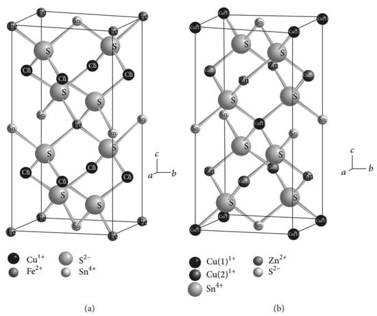
Copper–zinc–tin sulfide (Cu2ZnSnS4) films are becoming increasingly prominent for several reasons. These materials could replace indium and gallium in CIGS films, as their constituents are Earth-abundant and do not contain cadmium (toxic material). The experimental results showed that CZTS-based solar cells have an excellent absorption coefficients (more than 104 cm−1), tunable band gap values (1.45 eV to 1.6 eV), and greater stability in the kesterite phase (Figure 512) when compared with stannite and wurtzite. Researchers have reported that vacuum and non-vacuum deposition techniques have been used to produce CZTS films (Table 34). Further, they concluded that high-quality films could be synthesized using the vacuum-deposition method; however, this entails increased production costs.Figure 512.
Crystal structures of (
a
) stannite and (
) kesterite [207].
films (Table 45). It is noted that the non-vacuum deposition method offers an attractive cost-saving opportunity, higher deposition speed, and less waste of chemicals when compared with the vacuum-deposition technique. The obtained films could be employed for solar-cell applications because of long-term stability under solar radiation, excellent absorption coefficients (105 cm−1) in the visible light portion, and suitable band gap values (1.5 eV).
Table 34.
The growth of CZTS films using various deposition methods and the photovoltaic properties.
| Deposition Technique | Photovoltaic Properties | Reference | |||
|---|---|---|---|---|---|
| Voc (mV) | Isc (mA/cm2) | PEC (%) | FF (%) | ||
Table 45.
The growth of CuInX (X = S, Se, and Te) films using various deposition methods and the photovoltaic properties.
| Deposition Technique | Photovoltaic Properties | Reference | ||||||||||||||||
|---|---|---|---|---|---|---|---|---|---|---|---|---|---|---|---|---|---|---|
| Voc (mV) | Isc (mA/cm2) | PEC (%) | FF (%) | |||||||||||||||
| Pulsed-laser deposition | 376 | 38.9 | 5.85 | 40 | [166][208] | |||||||||||||
| Electrostatic spray deposition | 230 | 21.72 | 1.75 | 34 | [182][224] | |||||||||||||
| Chemical route | 521 | 19.13 | 6.17 | 62 | [167 | |||||||||||||
| Spray-coating method | - | - | ] | 1.1–1.9 | [209] | |||||||||||||
| - | [ | 183 | ] | [ | 225] | Nanoparticle ink technique | - | - | 2.1 | - | [168][210] | |||||||
| Electro-deposition method | - | - | 1.6 | - | [184][226] | Electro-deposition method | 563 | 14.8 | 3.4 | |||||||||
| Solution-coating process | 41 | 420 | ||||||||||||||||
| Rapid thermal-evaporative method | [ | 169 | ] | 36.39 | [211] | |||||||||||||
| 7.72 | 50.5 | CdSe | [ | 185 | ][227] | 222–501 | 0.17–6.45] | Pulsed hybrid electro-deposition method | 350 | 3.9 | 0.59 | 43 | [170][212] | |||||
| 0.02–1.88 | 50–58.1 | [ | 204 | Spin-coating method | - | - | 4.19 | - | [186][228] | 0.66–7.8 | 0.08–1.57 | 39.01–42.45 | [205] | Glancing angle-deposition method | 774 | |||
| 780 | ||||||||||||||||||
| - | 6.31 | - | [ | 192 | ][234] | |||||||||||||
| ] | [ | 246 | ] | |||||||||||||||
| Thermal-evaporative method | Sb2S3 | 330–470 | [ | 247 | ] | 23 | 11 | 61.9 | [138][180] | |||||||||
| Spin-coating method | - | - | 10 | - | [ | Sputtering method150 | -] | -[192] | 2.95–3.59 | |||||||||
| Hydrothermal method | In2S | - | [ | 171 | ||||||||||||||
| Electro-deposition method | 280 | ] | 34.06 | 320 | 23.43[ | 2.39 | 31.82 | Vapor-transport deposition | 806–839 | 20.2–21.6 | 12.5–13.5 | |||||||
| Vacuum evaporation method | 712 | 34.8 | 18.7 | 213 | ||||||||||||||
| ] | ||||||||||||||||||
| 0.41 | 36.72 | [ | 206 | ] | Sputtering and evaporation method73.3–76.9 | [139][181] | ||||||||||||
| [ | 187 | ] | [ | 229 | ] | [248] | - | - | 20.4 | - | [151] | SILAR method[ | - | -193 | 0.76–1.24] | - | [172][214] | |
| Pulsed electro-deposition | 440 | 33.5 | 5.2 | 38 | ||||||||||||||
| Hydrothermal method | Cu2SnS3 | 596 | [ | 188 | ][230] | 10.7 | 1.58 | 24.8 | [207][249] | Vapor-transport deposition | 683–839 | 22.2–22.9 | 9.2–14.4 | 60.6–75 | [140 | |||
| Vacuum evaporation | - | - | ] | 17.1 | [182] | |||||||||||||
| - | [ | 152 | ] | |||||||||||||||
| Sol–gel method | Cu2SnS3 | [ | 194 | ] | reactive-pulsed dc magnetron co-sputtering | 667 | 19.6 | 7.9 | 60 | [ | ||||||||
| Chemical liquid-deposition | 173 | ] | - | 276 | [215] | |||||||||||||
| - | 2 | - | [ | 189 | ][231] | 11.6 | 1.12 | 35 | [208][ | Sputtering method | - | - | 11.2 | - | [141][183] | |||
| 250 | ] | Co-precipitation method | 168.2 | 8.11 | 0.4 | 27.6 | [153] | Electro-deposition method[ | 204195 | 7.6] | 0.55 | 35.68 | [174][216] | |||||
| Doctor blade-coating method | - | - | 2 | - | [190 | |||||||||||||
| Pulsed-chemical vapor deposition | SnS | 244 | 19.4 | ] | 2.04[232] | 42.97 | [209] | Radio-frequency sputtering | - | - | 14 | |||||||
| [ | 251 | ] | Inkjet printing method | - | 386[142] | 29.78 | Spin-coating method[ | |||||||||||
| Radio-frequency sputtering | - | SnS | 184 | ] | ||||||||||||||
| 5.04 | - | 44 | - | [ | 154] | -[196] | 0.5–2.4 | - | Laser-ablation method | |||||||||
| Solvo-thermal method | [ | 175 | 130 | ] | [217] | 0.38 | - | [210 | Evaporation method | |||||||||
| 20.72 | 0.735 | 27.3 | ] | [ | 252 | ] | - | - | 10.6 | - | [155][197] | |||||||
| magnetron sputtering method | 666 | 7.9 | 2.26 | 43.39 | [176][218 | |||||||||||||
| Radio-frequency sputtering | ] | |||||||||||||||||
| [ | 191 | ] | [ | 233 | ] | SnS | 450 | 17.13 | 5.24 | 68 | [211][ | Electro-deposition method | - | Spin-coating method | 556- | 9.4 | - | [156][198] |
| 13.5 | 3.02 | 40.3 | [ | 177 | ] | |||||||||||||
| Spin-coating method | 253 | ] | [ | 219 | ] | Thermal co-evaporation method | - | - | 10.2 | - | ||||||||
| Solution processed | CuSbS2 | - | - | [ | 193][235] | Electro-deposition method | ||||||||||||
| 1.72 | - | [ | 212 | ] | [ | 254] | 666 | 30.5 | ||||||||||
| 15.4 | 75.6 | Spray pyrolysis | 246–421 | 3.9–10.3 | [157][199] | |||||||||||||
| 0.4–1.4 | 32.5–39 | [ | Ink-based deposition | 320 | 18.49 | 2.15 | 37 | |||||||||||
| Mechanochemical and doctor-blade technique | Cu4SnS4 | 178 | ] | [ | 220] | [194][236] | ||||||||||||
| 300 | 29.2 | 2.34 | 26 | [ | 213 | ][255] | Electro-deposition method | 413 | 32.5 | 6.6 | 49 | [158][200] | ||||||
| Spin-coating method | 520 | 112.52 | 0.28 | 26.75 | [179][221] | Ink-based deposition | - | - | ||||||||||
| chemical vapor deposition | PbS | 520 | 2.11 | 1.93- | 0.29[195][237] | Electro-deposition method | ||||||||||||
| 29 | [ | 214 | ] | [ | 256 | ] | 741 | 23.2 | 10.2 | 59.6 | [ | |||||||
| Pulsed-laser deposition | - | - | 159 | 6.62 | ][ | Co-precipitation method-201] | ||||||||||||
| [ | 180 | ] | [ | 222 | ] | - | - | 0.83–1.27 | - | [196][238] | ||||||||
| Nebulizer-spray method | PbS | - | - | 0.39 | - | [215][257] | Electro-deposition method | - | - | |||||||||
| Sulfurization technique | 610 | Colloidal synthetic method | 439–471124 | - | 0.65–1.45- | [ | - | |||||||||||
| Chemical-bath deposition | Ni3Pb2S | 4.5 | 160 | 262 | ][202[197][239] | |||||||||||||
| 610 | 9.9 | 2.7 | ] | |||||||||||||||
| [ | 181 | ] | [ | 223 | ] | 47 | [216][258] | Electro-deposition method | - | - | Solvothermal method4.5 | - | 268 | 4[161 | ||||
| Chemical-bath deposition | ZnTe | 150 | 0.75 | 56 | ][203 | [ | 25.6198 | 0.49] | ||||||||||
| ] | [ | 240 | ] | |||||||||||||||
| 24.86 | [ | 217 | ] | [ | 259 | ] | Electro-deposition method | - | - | 1.63 | - | [162][204] | ||||||
| Electro-deposition method | 480 | 20 | 4.13 | 43 | [199][241] | Electro-deposition method | - | 0.143–0.376 | 0.079–0.403 | 0.384–0.526 | [163][205 | |||||||
| Electro-deposition method | ] | |||||||||||||||||
| - | - | 3.4–3.8 | - | DC-magnetron sputtering method | 553 | 30.18 | 11.28 | 68 | [164][206] | |||||||||