Your browser does not fully support modern features. Please upgrade for a smoother experience.
Please note this is a comparison between Version 1 by Khaled Laadjal and Version 2 by Conner Chen.
The high performance, multi-functionality, and high integration of electronic devices are made possible in large part by the multilayer ceramic capacitors (MLCCs). Due to their low cost, compact size, wide capacitance range, low equivalent series inductance (ESL) and equivalent series resistance (ESR) and ESR, and excellent frequency response, MLCCs play a significant role in contemporary electronic devices.
- multilayer ceramic capacitors (MLCCs)
- high-power density
- failure mechanism
1. Introduction
Ceramic capacitors, film capacitors, and electrolytic capacitors are the three basic types of capacitors. The dielectric, structure, terminal connection technique, use, coating, and electrolyte may all be used to further classify each category (only for electrolyte capacitors) [1]. Since the number of stored charges is mostly dependent on the dielectric material, the dielectric categorization is the most used. Table 1 displays some of the above categories of dielectric properties [2][3][2,3].
| Capacitors Categories | Dielectric | Dielectric Constant (εr) | Dielectric Thickness (d) |
|---|---|---|---|
| Electrolyte | Aluminum Oxide | [8, 10] | [0.03, 0.7] μm |
| Tantalum Oxide | [23, 27] | [0.04, 0.5] μm | |
| Film | Polyester Film | ≅3.2 | [0.5, 2] μm |
| Ceramic | Barium Titanate | [0.5, 20] × 103 | [2, 3] μm |
| Titanium Oxide | [15, 250] | [2, 3] μm |
As it was previously possible to establish, the properties of the dielectric dictate how the capacitor behaves. This is generally the case for all capacitors, however for exceptionally high-power capacitors, the permeability of the plates, tabs, and connections may also be used to calculate the highest peak current of the capacitor.
Table 1 makes it abundantly evident that the various kinds of capacitors have varied properties, thus which capacitor to use relies on the properties of the circuit in which it will be used. The following are a few of the most crucial factors to take into account while making a decision [1]:
- ○
-
Ratted voltage, capacitances, price, volumetric efficiency, consistency and dependability of capacitances, longevity, and power density.
- ○
-
Current ripple ratting and maximum peak current.
- ○
-
Temperature range, insulating resistance, and leakage current.
- ○
-
Capacitor performance and resonance frequency (capacitance dependency with frequency and temperature, as well as its internal resistance).
The most common type of capacitor in electronics is a ceramic one, and the most popular type of these is called a multilayer ceramic capacitor (MLCC). Many electrical products, including computers and cell phones, use MLCCs. Three kinds of commercially available dielectrics can be distinguished: Categories I, II, and III [4].
Titanium oxide, which has the lowest dielectric constant of the ceramic technologies, is used as a dielectric in Class I dielectrics, which are also known as temperature compensated dielectrics (Table 1). These capacitors are useful for several electronic systems circuits, including snubber circuits and soft-start circuits, due to their poor volumetric efficiency and tiny capacitance values (100 nF). Along with being relatively stable with voltage, temperature, and time, the capacitance additionally has a low dissipation factor [5].
Class II dielectrics, also known as high dielectric constant materials, use the high dielectric constant material barium titanate as a dielectric (Table 1). These capacitors are produced due to their compact sizes and high capacitance values. Their dissipation factor is therefore relatively large, and their capacitance tends to be unstable in response to voltage, temperature, and time [2][3][4][2,3,4]. The maximum capacitance variation over a temperature range is determined by the final digit of the three-character alphanumeric code used to describe Class II dielectrics. For instance, because the maximum temperature change for the X5R, X7R, and X8R’s capacitance is 15%, these devices are recommended for use in power electronics circuits. Both classes have higher dielectric resistance and lower dissipation factors when compared to Al-caps, but they have worse properties when compared to MK capacitors. Class III dielectrics, which have the highest capacitance and maximum volumetric efficiency of the three classes, are used to construct barrier layer capacitors. However, temperature, voltage, and frequency have a significant impact on them. Additionally, they operate at a voltage of about 25 V. Class III ceramic capacitors are frequently used in bypass coupling when dielectric losses, strong insulation resistance, and stability are not required [4].
Class II and class III capacitors, which tend to have greater dielectric constants and smaller breakdown fields, are therefore better suited for low-voltage applications, particularly where considerable capacitance is needed. The failure of ceramic capacitors during dielectric breakdown, which renders the device worthless, is another pertinent component of these devices [6].
For power devices, Cer-aLinkTM, a new ceramic capacitor technology from EPCOS, may be the ideal option. Recent research has shown that this technology can be particularly useful in the DC-link of voltage source inverters because of its promising properties, including low losses, rising capacitance with applied voltage, low series inductance, and high-capacitance density [7][8][7,8].
The necessity for portable electronic devices that can be connected to high-speed, high-transmission-capacity networks has increased, as shown by words like “digital nomad”, “ubiquitous computing” and “internet of things.” These breakthroughs have accelerated research on electronic components with high performance, great reliability, and low power consumption. The multilayer ceramic capacitor (MLCC), which is one of them, is the most significant passive element capable of storing and releasing electrical charge. For resonant circuit applications, MLCCs provide excellent stability and low losses, as well as great volumetric efficiency for buffer, by-pass, and coupling applications [5][9][10][11][5,9,10,11].
Prior studies, including those conducted by the authors of [12] and [13][14][15][16][17][18][19][13,14,15,16,17,18,19], have evaluated an MLCC’s dependability under high-acceleration impacts, mostly focusing on structural failure for an MLCC’s electrical, mechanical, and thermal interaction [20]. Using a multiscale homogenization modeling method, the authors of article [21] created a finite element simulation model to describe the structural characteristics of multilayer ceramic capacitors. In [22], it was discovered that the electric field distortion brought on by the impact-driven deformation of an MLCC can quickly lead to ceramic capacitor failure. This was demonstrated using the analogous mechanical model. Through a dynamic experiment with a high-overload impact, an MLCC failed. The impact of this failure on an advanced system was then examined.
Energy-storage and conversion technologies are envisaged for use in practical applications because they have a wide operating temperature range, are inexpensive, have a high energy density, a high-power density, and a high conversion efficiency. Figure 1 illustrates the energy and power density requirements for typical energy-storage systems [23].
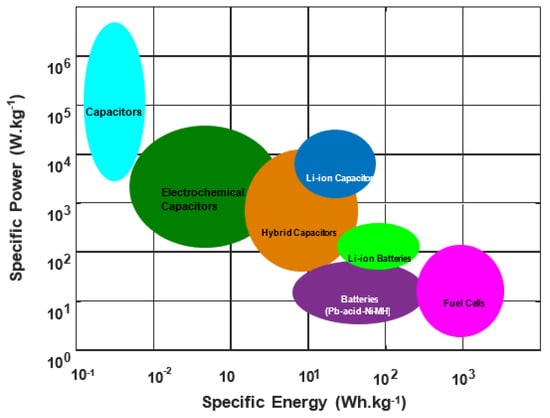
Dielectric capacitors offer ultra-high-power densities > 10 kW kg−1 in comparison to conventional energy-storage devices. As a result, they have ultra-high charging and discharging speeds and may start releasing accumulated energy in a nanosecond or microsecond time frame scale, allowing for exceptionally high pulse power. They also offer beneficial qualities, including an extremely long cycle life, dependability, and safety.
Dielectric capacitors are therefore essential for the development and application of third-generation semiconductor devices. These components are also utilized in high-power energy-storage and pulse power systems, which include electromagnetic weapons, advanced medical equipment, electric and hybrid vehicles, and smart grids [24][25][24,25]. However, the energy density of currently available commercial polymer dielectric capacitors is quite low (0.1 Wh.kg−1), leading to relatively large and heavy energy-storage and pulse-power devices.
For instance, the capacitors under each carriage of a high-speed train weigh more than 50 kg and occupy 50% of the space and 60% of the weight of the converter valves for high-voltage, direct-current transmission. This enormous volume would produce a significant equivalent series inductance (ESL) when switched quickly, which could harm or even cause the failure of semiconductor devices. This shows that these integrated capacitors cannot yet meet the specifications for use in electronic systems and devices that call for small, lightweight integrated capacitors [26][27][26,27].
2. MLCC and Its Fabrication Process
The exact structure and manufacturing procedure of the MLCCs are shown schematically in Figure 26. MLCCs are constructed by alternately layering numerous dielectric layers in tandem with inner electrodes. The inner electrodes are connected to the outside terminal for surface installation. In place of expensive Pd, base metals like Ni and Fe are increasingly used as inner electrode materials. The exterior termination is constructed of layers of Cu or Ag, Ni plating, and Sn plating. It is possible to express the MLCC capacitance as in Equation (1). When choosing the chip size and dielectric materials, the thickness of the dielectric layer and the number of stacked layers are important design considerations for MLCCs with high capacitance [28][92].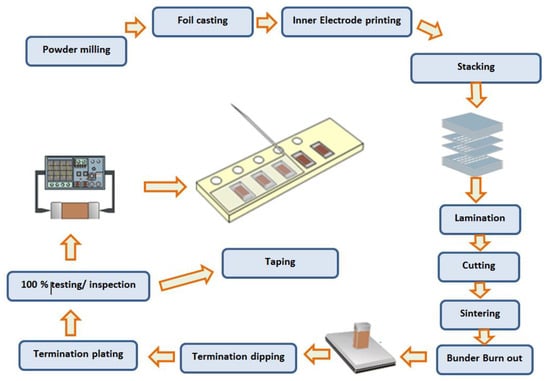
Figure 26.
MLCC architecture and fabrication process schematics.
- (1)
-
The use of silver (Ag)/Pd alloy electrodes having a high Ag content (more than 70%) to achieve low temperature sintering of the dielectrics.
- (2)
-
The use of base metals such as nickel (Ni) and copper (Cu) as internal electrodes by using a nonreducible dielectric that can be fired in a reducing atmosphere [38][109].The performance, dependability, and functionality of the electrode materials used in MLCCs are negatively impacted by residual stress, mechanical cracking from sintering shrinkage, and metal diffusion into the dielectric layer, all of which are caused by high sintering temperatures for dielectric materials. In order to avoid the oxidation of the base metal inner electrode, the green chips are additionally co-fired at low oxygen pressure. During sintering in a reducing environment, dielectric layers can experience a significant compositional change and defect development. The sintering environment must be meticulously regulated to minimize decrease of the dielectric material and to limit oxidation of the inner electrodes [39][40][33,95].Table 2.Different electrodes’ physical characteristics and price ratio.
Metals Melting Point (°C) Resistivity (mΩ) Price Ratio Ag 961 1.62 3 Cu 1080 1.72 1 Ni 1453 6.9 1 Pd 1552 10.4 80