Your browser does not fully support modern features. Please upgrade for a smoother experience.
Please note this is a comparison between Version 3 by Catherine Yang and Version 2 by Catherine Yang.
Contact selectivity is a key parameter for enhancing and improving the power conversion efficiency (PCE) of crystalline silicon (c-Si)-based solar cells. Carrier selective contacts (CSC) are the key technology which has the potential to achieve a higher PCE for c-Si-based solar cells closer to their theoretical efficiency limit. A recent and state-of-the-art approach in this domain is the tunnel oxide passivated contact (TOPCon) approach, which is completely different from the existing classical heterojunction solar cells. The main and core element of this contact is the tunnel oxide, and its main role is to cut back the minority carrier recombination at the interface.
- carrier selective contacts
- contact resistance
- tunnel oxide passivated contact
- renewable energy
1. Introduction
Meeting the world’s growing energy demands while simultaneously tackling human-induced global warming has become one of the indisputable challenges that humanity is going to face around the globe in the near future. This requires sustainable energy production from clean and eco-friendly resources. Solar photovoltaic (PV) technology is gaining favorable attention, and this is clearly reflected in the global statistics of the total installed capacity of solar PV modules. Currently, the worldwide cumulative installed capacity of PV modules has already exceeded 700 GW, and its significant increase is expected in the coming years [1][2]. The unique features, such as non-toxicity, abundance, and long-term stability of crystalline silicon (c-Si), have made it a market-dominant technology since the very beginning, with an almost 95% market share [3]. The cost of a c-Si PV module is approximately one-half of the PV system cost and is mainly dominated by material costs, especially by the costs of the Si wafer [4]. On the other hand, the cell manufacturing cost is about one-quarter of the module cost, making it about one-eighth of the complete PV system’s cost [4]. Therefore, besides improved production technology, increasing the efficiency of the cell has significant potential to bring down the system costs even more.
To improve the power conversion efficiency (PCE) of c-Si solar cells closer to its thermodynamic limit of ~29.4% [5], one of the key and fundamental requirements is to improve the photogenerated minority carrier lifetime ( ) by minimizing the recombination losses. As the bulk minority carrier lifetime ( ) in state-of-the-art float-zone (FZ) c-Si wafers has already exceeded 30 ms [6], most of the recombination losses occur at the metal contacts. Therefore, minimizing the contact losses in c-Si solar cells through surface passivation have been an active area of research in recent years. Previously, contact recombination was minimized by introducing a highly doped localized back surface field in a passivated emitter rear locally diffused (PERL) homojunction solar cell. Although PERL solar cells have achieved remarkable efficiency ( ) of ~25% [7], their high fabrication cost (~0.071 [8]) and low thermal barrier for recombination current carriers at the back has moved researchers towards alternative cost-effective and heterojunction-based approaches.
2. Structure and Electrostatics of TOPCon Solar Cell
According to ITRPV, high efficiency and state-of-the-art PERC, along with its variants (e.g., PERL), dominated the PV market with a ~80% share in 2020 [9]. Opportunities exist for those technologies that promise lower production costs with minimal changes to the existing production lines for PERC solar cells. As the fabrication of TOPCon technology cells just adds a few steps in the existing manufacturing units of PERC cells [4][10], therefore it is fundamentally compatible to replace PERC solar cells.
The two-dimensional (2-D) schematic diagram of the TOPCon solar cell is shown in Figure 1. It is produced with c-Si, which has a p-n junction with a heavily p-doped emitter on the front side and an n-type substrate [10].
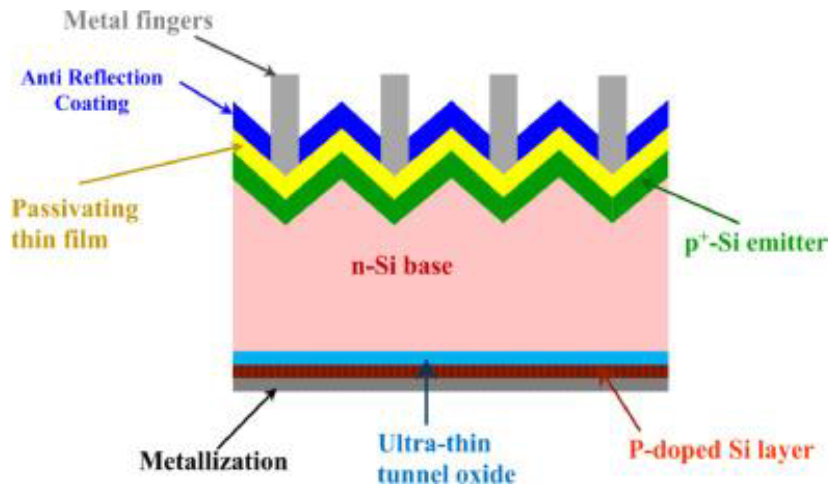
Figure 1. Two-dimensional schematic of an n-type c-Si-based TOPCon solar cell [11].
At the front surface, the layer is used as an anti-reflecting coating, whereas a thin layer of aluminums oxide ( ) is used for the passivating layer, reducing the surface recombination velocity below 50 cm/s [12][13]. At the back, an ultrathin ( ) tunneling layer of is used as an electron transport layer, whereas a thin layer of the heavily n-doped poly-Si layer is used to provide an Ohmic contact at the back and electric field for the photogenerated electrons to tunnel through the layer [14].
3. Configurations of the TOPCon in c-Si-Based Solar Cells
There are two different types of configurations possible for the TOPCon, which can be used as a rear contact in c-Si-based solar cells. These are the following:
-
n-TOPCon rear contact for n-type c-Si solar cell
-
p-TOPCon rear contact for p-type c-Si solar cell.
3.1. n-TOPCon Rear Contact for n-Type c-Si Solar Cell
The PV cell structure of the n-TOPCon, which is used as a rear contact for the n-type c-Si-based solar cells [13], is shown in Figure 1. The structure contains tunnel oxide, which is developed and grown in nitric acid [15], with a layer of P-doped silicon. Afterward, the a-Si layer was deposited, and the contact was further strengthened and hardened through an annealing process at a very high temperature, which ranges between 800 °C and 900 °C. After annealing, this structure was exposed to hydrogen passivation for a duration of about 30 min at a temperature of 400 °C [16]. The n-type TOPCon structure is used as a rare contact in the n-type c-Si-based solar cell, which has achieved the highest efficiency of up to 25.7% at the cell level [17]. Additionally, it provides extremely excellent and outstanding surface passivation at the Schottky interface. Moreover, it also reduces the contact resistance at the interface [18][19].
3.2. p-TOPCon Rear Contact for p-Type c-Si Solar Cell
The cell structure of the p-TOPCon used as a rear contact for the p-type c-Si-based solar cells consists of a full-area TOPCon emitter at the rear contact with an oxide layer [11][20], as shown in Figure 2. This structure is designed by using the method of a wet-chemically grown silicon oxide (SiOx) layer, which is an extremely thin layer. Moreover, it is also covered with a thick layer of phosphorous-doped silicon carbide (SiC). The thickness of this layer is equal to 15 nm, and it is deposited by using the process of plasma-enhanced chemical vapor deposition (PECVD), which was further strengthened and hardened through an annealing process in a tube furnace at a high temperature of up to 800 °C [13]. The p-type TOPCon structure was used as a rare contact in the p-type c-Si-based solar cell and achieved the very best efficiency at the cell level of ~24.3% [20]. The conversion efficiency of the p-TOPCon used as a rare contact is lower than that of the n-TOPCon. The main reason for this reduction is a slightly increased or magnified series resistance at the interface compared to that of n-TOPCon as a rear contact.
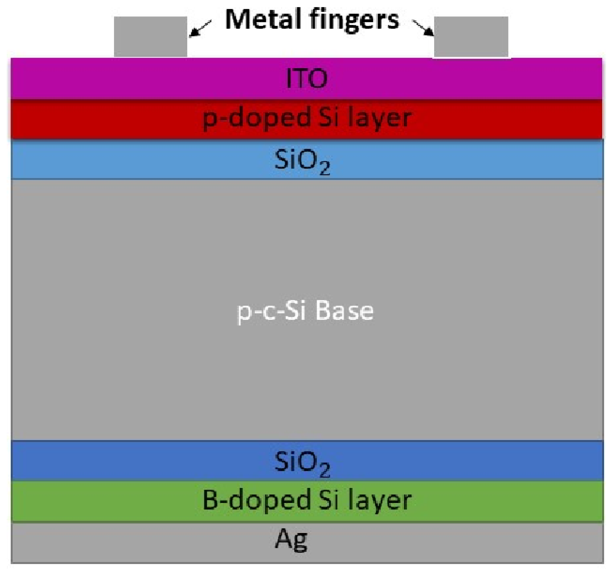
Figure 2. Schematic diagram of p-type c-Si TOPCon solar cell [11].
4. Fabrication of TOPCon Solar Cell
The TOPCon solar cell is mostly produced on a phosphorus-doped c-Si wafer obtained through the Czochralski (CZ) method [21], as shown in Figure 3. This is because low amounts of oxygen are required for phosphorus-doped wafers with [22]. The steps involved in the assembly for the fabrication of the TOPCon cell are presented in Figure 3 in the form of boxes. First of all, the c-Si wafer is double-sided textured with irregular pyramids using a potassium hydroxide (KOH) solution, which is described by the “Texture” box as shown in Figure 3. After standard RCA (Radio Corporation of America) cleaning, the wafer is kept in a boron diffusion furnace to form the boron-doped (or p-type) emitter using a boron tribromide ( BBr3) source. Then, by using a hydrofluoric acid and nitric acid ( HF/HNO3) solution, the bottom boron-doped emitter is removed through a single-side etching process. In the next step, the wafer is cleaned using chemicals, and then a stack of passivation layers consisting of ultrathin and intrinsic poly-Si layers is developed, which is described by thermal +i-poly and SSE+ cleaning tabs, as shown in Figure 3. The layer is thermally grown, whereas the poly-Si layer is developed in a low-pressure chemical vapor deposition (LPCVD) system. Then, intrinsic poly-Si is n-doped in a phosphoryl chloride ( SiOx) diffusion furnace. The front side of the wafer is cleaned from poly-Si through another single-side etching process. The wafer is again cleaned through the RCA process, and then an anti-reflection and passivation layer is formed in front of the boron-doped emitter. A layer of using PECVD is formed on the back to protect and the poly-Si passivation stack. In the last step, an H-shaped metal contact with nine busbars is formed on both sides using screen printing and high-temperature (~760°C ) firing methods in order to provide metal contacts [20]. After fabrication, the current voltage ( ) and other valuable characteristics are measured under the standard solar spectrum of AM1.5G (1000w/m2 ) using some suitable flasher instruments.
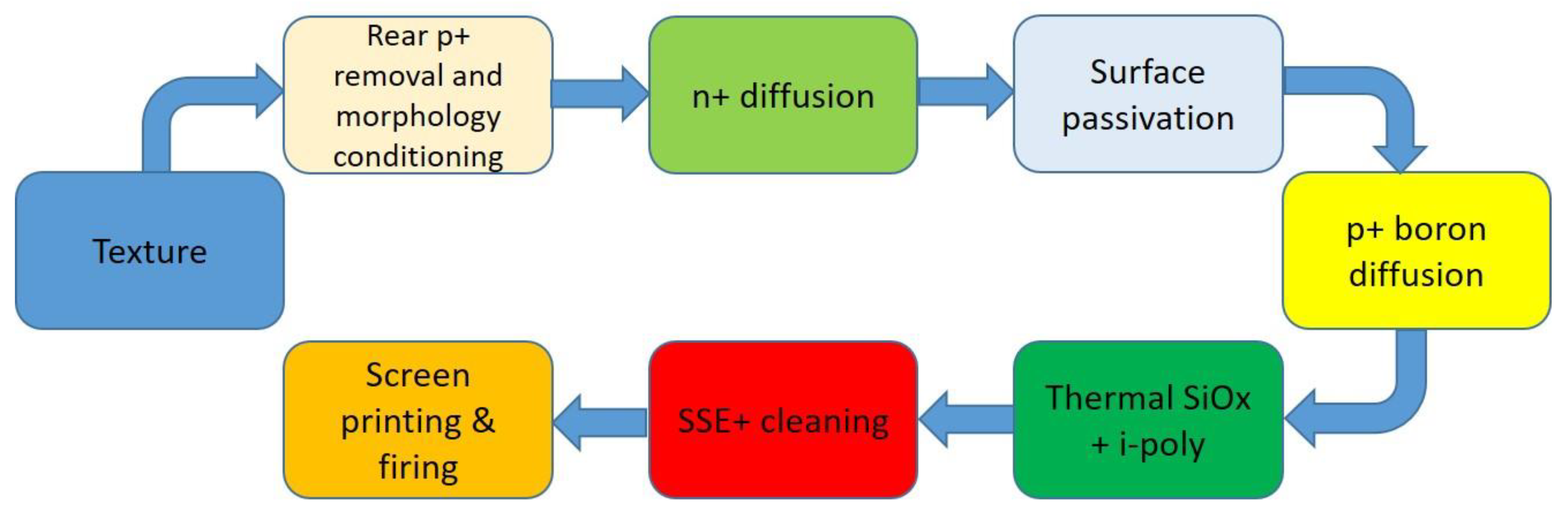
Figure 53. Process flow of TOPCon solar cells.
References
- International Energy Agency (IEA) Home Page. Available online: https://iea.blob.core.windows.net/assets/1a24f1fe-c971-4c25-964a-57d0f31eb97b/Renewables_2020-PDF.pdf (accessed on 26 November 2022).
- The International Renewable Energy Agency (IRENA) Home Page. Available online: https://www.irena.org/-/media/Files/IRENA/Agency/Publication/2021/Apr/IRENA_-RE_Capacity_Highlights_2021.pdf?la=en&hash=1E133689564BC40C2392E85026F71A0D7A9C0B91 (accessed on 23 November 2022).
- Fraunhofer Institute for Solar Energy Systems (ISE) Home Page. Available online: https://www.ise.fraunhofer.de/content/dam/ise/de/documents/publications/studies/Photovoltaics-Report.pdf (accessed on 23 November 2022).
- Blakers, A. Development of the PERC solar cell. IEEE J. Photovolt. 2019, 9, 629–635.
- Richter, A.; Hermle, M.; Glunz, S.W. Reassessment of the limiting efficiency for crystalline silicon solar cells. IEEE J. Photovolt. 2013, 3, 1184–1191.
- Cuevas, A.; Macdonald, D.H. Measuring and interpreting the lifetime of silicon wafers. Sol. Energy 2004, 76, 255–262.
- Green, M.A. The Passivated Emitter and Rear Cell (PERC): From conception to mass production. Sol. Energy Mater Sol. Cells. 2015, 143, 190–197.
- Kumar, A.; Bieri, M.; Reindl, T.; Aberle, A.G. Economic viability analysis of silicon solar cell manufacturing: Al-BSF versus PERC. Energy Procedia 2017, 130, 43–49.
- International Technology Roadmap for Photovoltaic (ITRPV) Home Page. Available online: https://itrpv.vdma.org/documents/27094228/67038244/2021-04-29%20PR%20VDMA%20PV%20ITRPV%202021%20EN_1619690887765.pdf/644380bd-85a3-99d9-e25f-c4ccc6556e64 (accessed on 23 November 2022).
- Wilson, G.M.; Al-Jassim, M.; Metzger, W.K.; Glunz, S.W.; Verlinden, P.; Xiong, G.; Mansfield, L.M.; Stanbery, B.J.; Zhu, K.; Yanfa, Y.; et al. The 2020 photovoltaic technologies roadmap. J. Phys. D. 2020, 53.
- Ghosh, D.K.; Bose, S.; Das, G.; Acharyya, S.; Nandi, A.; Mukhopadhyay, S.; Sengupta, A. Fundamentals, present status and future perspective of TOPCon solar cells: A comprehensive review. Surf. Interfaces 2022, 30, 101917.
- Kafle, B.; Goraya, B.S.; Mack, S.; Feldmann, F.; Nold, S.; Rentsch, J. TOPCon–Technology options for cost efficient industrial manufacturing. Sol. Energy Mater. Sol. Cells 2021, 227, 111100.
- Yang, X.; Weber, K. N-type silicon solar cells featuring an electron-selective TiO2 contact. In Proceedings of the 2015 IEEE 42nd Photovoltaic Specialist Conference (PVSC 2015), New Orleans, LA, USA, 14–19 June 2015; pp. 1–4.
- Younas, R.; Imran, H.; Shah, S.I.; Abdolkader, T.M.; Butt, N.Z. Computational modeling of polycrystalline silicon on oxide passivating contact for silicon solar cells. IEEE Trans. Electron. Devices 2019, 66, 1819–1826.
- Yang, X.; Bi, Q.; Ali, H.; Davis, K.; Schoenfeld, W.V.; Weber, K. High-performance TiO2-based electron-selective contacts for crystalline silicon solar cells. Adv. Mater. 2016, 28, 5891–5897.
- Macco, B.; Vos, M.F.; Thissen, N.F.; Bol, A.A.; Kessels, W.M. Low-temperature atomic layer deposition of MoOx for silicon heterojunction solar cells. Phys. Status Solidi RRL Rapid Res. Lett. 2015, 9, 393–396.
- Masuko, K.; Shigematsu, M.; Hashiguchi, T.; Fujishima, D.; Kai, M.; Yoshimura, N.; Yamaguchi, T.; Ichihashi, Y.; Mishima, T.; Matsubara, N.; et al. Achievement of more than 25% conversion efficiency with crystalline silicon heterojunction solar cell. IEEE J. Photovolt. 2014, 4, 1433–1435.
- Bivour, M.; Temmler, J.; Steinkemper, H.; Hermle, M. Molybdenum and tungsten oxide: High work function wide band gap contact materials for hole selective contacts of silicon solar cells. Sol. Energy Mater. Sol. Cells 2015, 142, 34–41.
- Feldmann, F.; Bivour, M.; Reichel, C.; Hermle, M.; Glunz, S.W. A passivated rear contact for high-efficiency n-type silicon solar cells enabling high Vocs and FF > 82%. In Proceedings of the 28th European PV Solar Energy Conference and Exhibition, Villepinte, France, 30 September–4 October 2013; pp. 988–992.
- Battaglia, C.; De Nicolas, S.M.; De Wolf, S.; Yin, X.; Zheng, M.; Ballif, C.; Javey, A. Silicon heterojunction solar cell with passivated hole selective MoOx contact. Appl. Phys. Lett. 2014, 104, 113902.
- Kiaee, Z.; Fellmeth, T.; Steinhauser, B.; Reichel, C.; Nazarzadeh, M.; Nölken, A.C.; Keding, R. TOPCon Silicon Solar Cells with Selectively Doped PECVD Layers Realized by Inkjet-Printing of Phosphorus Dopant Sources. IEEE J. Photovolt. 2021, 13, 31–37.
- Feldmann, F.; Simon, M.; Bivour, M.; Reichel, C.; Hermle, M.; Glunz, S.W. Efficient carrier-selective p-and n-contacts for Si solar cells. Sol. Energy Mater. Sol. Cells 2014, 131, 100–104.
More