Сhallenge for spintronics is to find new ways for the control of electronic phenomena and magnetic properties of solids at nanoscale. Some promising aspects are connected with developing new materials. The resviearchw highlights the areas devoted to the creation of new functional materials for spintronics based on magnetic semiconductors and demonstrates the technical possibilities of creating various devices, in particular, a maser, a p-n junction with a colossal magnetoresistance, a spin valve, a magnetic lens, modulators, spin wave amplifier, etc. A magnetic semiconductor is a magnetic material that, in terms of specific conductivity, occupies an intermediate position between a conductor and an insulator, and has a band gap comparable to ~ A magnetic semiconductor is a magnetic material that, in terms of specific conductivity, occupies an intermediate position between a conductor and an insulator, and has a band gap comparable to ~kBT. Most known magnetic semiconductors (SC) are either oxides or chalcogenides (sulfides, selenides and tellurides) of 3d transition metals, rare earth 4f metals or a combination. Spintronics (spin electronics) studies spin current transfer (spin-polarized transport) in condensed media, including contact structures, heterostructures, superlattices and multilayers. Much attention is paid to the mechano-physical methods of obtaining of high-density transparent nanoceramics based on magnetic semiconductors. The potential possibility of using nanoceramics as an absorber of solar energy, as well as in modulators of electromagnetic radiation, is also presented. The THz magneto-optics in magnetic semiconductors is shown to be beneficial to the intensively developing fields of spintronics – ultrafast magnetooptics and magnetophotonics in magnetic semiconductors.
- spintronics
- magnetic semiconductors
- complex magnetic oxides
1. Introduction
2. Nanocrystalline Magnetic Semiconductors—New Functional Materials for Spintronics
Nanocrystalline magnetic SCs are of interest both for fundamental problems of condensed matter physics and for practical applications, due to the appearance of new properties, when the particle size of a SC is reduced to the nanometer scale [52][53][54][112,113,114]. For the past decade the development of magnetic materials, particularly manganites and ferrites in nano-form, has undergone a fast evolutionary growth as strategic materials in spintronics and sensor applications [55][56][57][58][115,116,117,118]. At the same time, the concentration of defects in nanomaterials is much higher than in equilibrium single or polycrystals. This factor also significantly determines the properties of nanomaterials, transforming nanosized magnetic SCs into multifunctional materials. The features and the possibility of using nanosized ferromagnetic SCs as functional materials are well studied. Meanwhile, similar features are also manifested in nanosized antiferromagnetic SCs. For example, the presence of linear dichroism (~50%) allows for the use of antiferromagnetic semiconductor CuO as polarizers of infrared radiation [59][119]. Electron-field emission in CuO nanofibers is recommended for use in displays [60][120]. Irradiated nanocrystalline CuO oxides can accelerate reaction-catalytic effects in the production, for example, of alcohols. Moreover, the synthesis rate, for example, of copper phthalocyanine, can be controlled by a magnetic field at room temperature [61][62][121,122]. Nanocrystalline CuO is used in electronics as a buffer layer in complex thin-film electronic nanodevices [63]. Moreover, it can enhance an electrochemical activity, which is promising for use as electrodes in lithium current sources [64][123] and as an analyzer of carbon dioxide concentration [65][124]. However, there are problems in obtaining high-quality optically transparent SC nanomaterials of various types (powder, ceramic, fiber, and film).2.1. High-Density Magneto-Optical Nanoceramics
For creating ceramics from a nanocrystalline material, important conditions are the preservation of the composition and size of compacted particles. Since magnetic SCs are multicomponent compounds, the production of high-density nanoceramics is rather complicated. To create nanoceramics, dynamic and static loading methods for obtaining high-density bulk nanomaterials are used. Static loading refers to the method of severe plastic deformation—shearing under pressure of at least 8 GPa. In this method, the number of distortions is determined not only by the applied high static pressure, but also by the angle of rotation of the anvils. For the creation of nanoceramics based on magnetic SCs, special high-pressure chambers were developed [66][67][125,126]. For example, using the static deformation method, LaMnO3+y nanoceramics with a density of 99% and grain sizes close to those of a nanopowder can be obtained [68][127]. It was also found that at high degrees of deformation and small crystallite sizes, the magnitude of micro-deformations in nanoceramics decreases, which may be due to more efficient relaxation of lattice stresses by grain boundary sliding with a decrease in crystallite size. Dynamic loading refers to the method of explosive action on a low-density (polycrystalline powder compact) coarse-grained material made of a magnetic SC by spherically converging shock waves, as well as pressing axially-symmetric workpieces under the action of an explosion [69][70][67,128]. When exposed to spherically converging shock waves, the material is placed in a spherical steel hermetic case, in which, at the moment of a spherical explosion, the material is simultaneously compressed in all ways and a nanostructure is formed. During explosive pressing of axially-symmetric workpieces, the material is placed in a steel cylinder, in which, at the moment of explosion, the detonation wave propagates along the generatrix axis. The integrity of specially designed metal covers is not violated, which protects the resulting nanoceramics from contamination. The created nanoceramics show high temperature- and time-stability. As a result, the advantage of the developed methods is the ease of implementation, the combination of the creation of a nanostructure and material compaction in a single process, the production of high-density (~99%) stable nanosized materials and the absence of external contaminants. The results can be used for obtaining nanoceramics from a wide range of materials. Some fragments of real SC nanoceramics prepared by various methods are shown in Figure 217. It can be seen that the described methods allow obtaining dense nanomaterials of quite large geometrical sizes.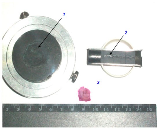
2.2. Nanocrystalline Y
3
Fe
5
O
12
as a New Magneto-Optical Material
An optically transparent high-density (density 99.6%) Y3Fe5O12 (YIG) nanoceramic (Figure 217) was obtained by means of a sheared static pressure of ~50 GPa. The authors of [77][78][135,136] showed that the absorption coefficient of nanoceramic Y3Fe5O12 in the transparency window is below 50 cm–1. It is mainly due to light scattering by crystallites and varies slightly with reduction of grain size. As the degree of deformation of YIG nanoceramics increases, the concentration of defects changes and the magnitude of micro-deformations decreases. However, these factors have only little effect on the absorption coefficient in the transparency window. Figure 318 shows that the value of the Faraday rotation for nanoceramics of YIG is only 1.5 times less than that for the YIG single crystals and exceeds 50 deg/cm. It is important that as the grain size decreases, the Faraday effect increases, and then, starting from a grain size of 21 nm, the effect decreases again. The observed increase of the Faraday effect in nanosized magnetic SCs was theoretically explained in [79][137]. It was shown that electric dipole transitions in clusters of mixed valences of 3d ions in nanosized magnetic materials with the structure of perovskite and garnet can lead to a resonant enhancement of the MO activity in the limited area of deformations. Finally, transparent high-density nanoceramics based on magnetic SCs can be widely used for creation of various high-frequency and microwave sensors and shields and MO devices, in particular, IR radiation modulators, displays, etc.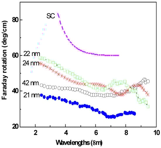
2.3. Nanocrystalline CuO as a Material for Selective Solar Energy Absorbers
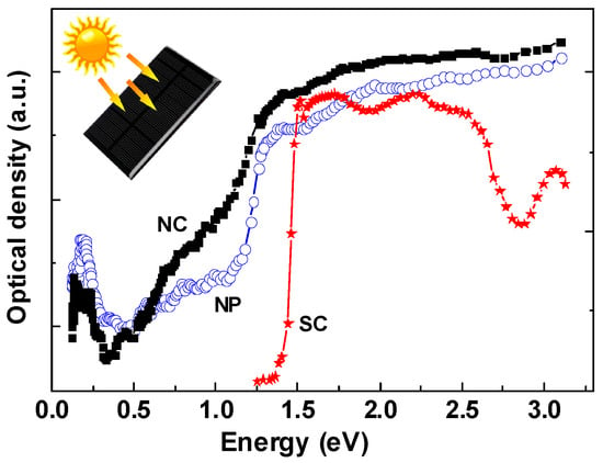
In relation to the problem of energy saving, great interest has arisen in alternative green energy sources, in particular, in selective absorbers of EM radiation and thermal converters of solar energy with coatings based on selective absorbers [80][138]. A selective solar energy absorber must meet certain requirements. For example, it should have a large absorption coefficient and a low reflection coefficient in the spectral range of solar radiation—in the energy range E > 0.5 eV. On the other hand, the absorber should have low electromagnetic energy emission or high reflectance at E < 0.5 eV. In other words, a selective absorber must absorb the energy of the radiation source as efficiently as possible but minimally re-emit it back into the atmosphere in the IR region of the spectrum. It was shown that copper oxides [81][82][83][139,140,141] can be used as selective absorbers in solar energy collectors with working temperatures up to T~500 °C. However, these materials do not meet the above conditions well, since they have a large forbidden gap. The authors of [84][85][142,143] demonstrated that this problem can be solved by changing the absorption spectrum of CuO practically without changing the refractive index when the copper oxide is transferred to the nanocrystalline state. Figure 419 shows the optical density (absorption) spectra for CuO single-crystal, nanopowder and nanoceramic, respectively.