Your browser does not fully support modern features. Please upgrade for a smoother experience.
Please note this is a comparison between Version 1 by Mohit Kumar and Version 3 by Catherine Yang.
Photoelectrochemical water splitting is a promising approach to sustainable hydrogen production with no carbon emissions. Hydrogen being a future fuel to coming human generations is of utmost importance. The photocathodes in a photoelectrochemical (PEC) water-splitting cell are essential for the direct evolution of hydrogen. Among the known photocathodes, Cu-based p-type semiconducting materials are the most promising photo-absorber materials owing to their low-cost, low toxicity, natural abundance, suitable band-gaps, and favorable band edges for reduction.
- photocathode
- H2 production
- PEC
- cocatalyst
- Hydrogen
- Nanomaterials
1. Introduction
The global energy demand is rising daily, while the supply comes from the same non-renewable energy sources [1]. Carbon emissions and environmental damage are liabilities of the energy derived from fossil fuels. However, the diminishing fossil fuel sources do not provide a steady fuel supply to meet the growing population and demand. Alternative energy sources should be considered to mitigate the impact of carbon emissions and meet the energy demand. H2 is considered a fuel for future generations with a high energy density and a lower molecular weight. At the moment, the majority of H2 is being produced using non-renewable sources of energy processes, such as steam methane reforming, coal gasification, and coal pyrolysis. In comparison, renewable sources of H2 production include biomass gasification & pyrolysis, thermochemical, solar-driven plasmolysis, and photo-electrolysis [2]. Presently, renewable energy sources are being scrutinized for developing reliable energy sources with no carbon emissions and a sustainable environment [3][4][3,4]. Solar energy-based technologies are attracting a vast number of applications in the form of renewable sources of energy. Solar-driven water splitting, or photoelectrochemical (PEC) water splitting, is one of the most attractive techniques used to decompose water into hydrogen (H2) and oxygen (O2) [5][6][5,6]. The energy falling on the earth’s surface from solar radiation is a driving force for H2 production. PEC cells use photoactive materials coated over a transparent conductive oxide surface, mainly known as a photoanode (where oxidation of water occurs on the surface resulting in the oxygen evolution reaction OER) and photocathode (where water reduction occurs on the surface, resulting in hydrogen evolution reaction (HER)) [7][8][7,8]. The photoactive material coated films over the photoanode are generally n-type semiconductor materials and p-type semiconductor materials on the photocathode.
PEC water splitting is also known as “artificial photosynthesis.” The concept of this phenomenon is nature-inspired plant leaves that convert solar light into carbohydrates. The sunlight absorbed by plant leaves is utilized by photosystem I (PS I) and photosystem II (PS II) to generate and transfer electrons through a series of transfer processes across several redox systems, to reduce CO2 to hydrocarbons [9]. Similarly, semiconductors, absorbing the minimum threshold wavelength of light equivalent to their bandgaps, generate photoexcited electron/hole (e−/h+) pairs, and the photoexcited electrons are diffused to the conduction band. Holes remain in the valence band of semiconductors, and electrons travel to the surface of the photocathode. The HER and OER occur on the surface of the photoelectrodes, and the active surface sites govern the kinetics of the reaction. The active surface sites contribute toward the adsorption of H+ and OH− molecules on the surface of the photoelectrodes [10][11][12][10,11,12].
The seminal report on PEC water splitting, in 1972, used a thin layer of TiO2 (Eg ~ 3.2 eV) as a photoanode for a PEC half-cell. Since then, photoanodes have been studied extensively with several material modifications and fabrication techniques. The OER takes place on the photoanode while the H2 evolution occurs on the counter electrode [13]. The n-type semiconductors, such asTiO2 (3.2–3.4 eV) [14], BiVO4 (2.2–2.4 eV) [15], WO3 (2.6–3 eV) [16], g-C3N4 (2.5–2.8 eV) [17], CdS (2.2–2.4 eV) [18], SrTiO3 (3.2–3.4 eV), and Fe2O3 (2–2.2 eV) have been widely applied for the photoanode application in the PEC cell. Among all of these materials, TiO2 comes out as the best material in terms of stability, while BiVO4 is the best material in abundance and light-absorbing capacity in the visible region [19].
Moreover, photocathodes have received very little attention when compared to photoanodes. Meanwhile, the direct evolution is more crucial than indirect evolution of H2, which occurs in the photoanodic half-cells. Developing a p-type semiconductor material with a suitable bandgap, band alignment, and stability toward the oxidizing environment is paramount. Along with these physical and optical characteristics, the semiconductor must be tested for applications using non-precious and earth-abundant metals that are neither poisonous nor harmful with a sustainable approach[20][21][22][23][24][20,21,22,23,24].
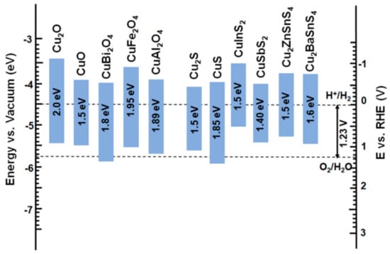
Figure 1. Energy band diagram of the various Cu-based binary, ternary, and quaternary metal oxides and sulfides.
Copper-based oxide/chalcogenide semiconductor materials are promising materials owing to their tunable band gaps, band alignment with respect to water reduction potential (Figure 1), absorption coefficients, and various synthesis procedures. In this rentry, the researchers hview, we have discussed recent advancements in the synthesis and fabrication of earth-abundant copper-based oxides/chalcogenides as a functional photocathode material for solar-driven water splitting, in light of their prospective use in PEC solar-to-hydrogen systems. In addition, several modifications that took place over a period and critically assess the ongoing debates in this area, have been discussed. Finally, this evaluation provides a chance to compare Cu-based semiconductor materials to give increasing emphasis to visible light-driven solar water electrolysis.

Figure 1. Energy band diagram of the various Cu-based binary, ternary, and quaternary metal oxides and sulfides.
2. Photocathode in a PEC Cell
Photocathodes are responsible for the reduction in a PEC cell serving the purpose of the direct evolution of hydrogen in a 2e− transfer process over its surface. The minority charge carriers drive the reaction on the surface of the photoelectrode. To date, a number of materials have been investigated as efficient photocathodes for hydrogen generation such as p-Si (Eg = 1.1 eV) with a theoretical maximum photocurrent density −44 mA/cm2 [25][26], InP (Eg = 1.3 eV) with a theoretical maximum photocurrent of −35 mA/cm2 [26][27], p-GaP (Eg = 2.2 eV) [27][28] Sb2Se3 (Eg = 1.2 eV) [28][29], BiSbS3, a p-type material with narrow bandgap (Eg = 2.2 eV)[29][30]. Cu-based photocathode materials have a suitable conduction band maximum for the reduction of H+ ions and bandgap. The non-toxicity, earth abundance, low-cost, high absorption coefficient, and ease of synthesis make them a promising and sustainable component for photoabsorber materials. The sluggish reaction kinetics of the HER and the recombinations require the engineering of the interfaces with the different layers which give several advantages.
3. Photocathode Materials
3.1 Cu-Based Metal Oxides for the Photocathode
Copper-based metal oxides, such as Cu2O and CuO are among the studied metal oxides, owing to their non-toxicity, availability, nature, and bandgaps. Due to their unique optoelectronic properties, they have been extensively used in energy conversion, storage, and sensing devices. However, the chemical instability of these materials restricts their PEC performance [30][31]. Cu2O has a narrow bandgap (Eg = 2.0 eV) with a theoretical photocurrent density of −14 mA/cm2 and a 18% photoconversion efficiency (PCE) owing to its light absorption in the AM 1.5 spectrum [31][32]. Cu2O, as a photocatalyst, showed a stable H2/O2 evolution for 1900 h in visible light (λ > 460 nm) [32][33]. Although Cu2O presents an immense opportunity for the hydrogen evolution, the photodegradation and recombination rate limits its photoactive material usage. Several strategies, including surface passivation, interfacial engineering, and cocatalyst decoration, have been investigated to overcome photodegradation and suppress the recombination to fabricate efficient photocathodes [33][34].
A Cu2O/CuO heterojunction photocathode modified with a Cu2S-Pt composite exhibited an enhanced hydrogen evolution. The optimum Cu2S and Pt used as cocatalysts deposited using SILAR and sputtering sequentially, facilitated the charge transport and suppressed recombination. Cu2O/CuO/Cu2S-9/Pt delivered J = −5.7 mA/cm2 at 0 VRHE (2.5 times of Cu2O/CuO), while a higher onset potential (Eop) for Cu2O/CuO/Cu2S−9/Pt was ~0.64 VRHE observed, compared to Cu2O/CuO (Eop = 0.54 VRHE). The excessive Cu2S deposition resulted in a parasitic light absorption and the creation of the recombination centers, resulting in Jph fading [34][38].
The back contact material is essential in suppressing the recombination and charge transfer. Au is the best contact material for Cu2O due to its large work function aligned with the valence band of Cu2O. Recently, a CuO/NiO-based composite was investigated in place of Au using sputtering and aerial oxidation for the back contact with Cu2O. A CuO/NiO thin film significantly improved and enhanced the transparency and hole collection (electron blocking) at the back contact of the Cu2O photocathodes [35][39].
CuO is a p-type semiconductor with a narrow bandgap (Eg = 1.3–1.7 eV) suitable for light absorption and H2 evolution. However, the photo corrosion of CuO in the presence of light is a significant drawback for the application. The majority of Jph for the CuO photocathode is due to the photo corrosion of CuO to Cu with a low faradaic efficiency of the HER (0.01%) [36][43]. The deposition of CdS (buffer layer) and TiO2 (as a protective layer), and Pt as a cocatalyst sequentially resulted in an enhanced PEC performance and faradaic efficiency (~100%) [36][43]. Various methods have been developed to synthesize CuO having different morphologies and bandgaps. The synthesis of CuO layers using sputtering and using variable power and thickness, exhibited a different photoactivity for hydrogen evolution. The variable power of sputtering (i.e., 30, 100, 200, and 300 W) in the synthesis resulted in a different morphology of the fabricated films, while the thickness of the layer of CuO played a role in light absorption. PXRD patterns showed the poor crystallinity of CuO due to low kinetic energy for diffusion and formation of Cu-O bond, while at higher the sputtering power, good crystalline films were obtained [37][44]. The deposition of a protective and stable metal oxide layer has proven to improve the faradaic efficiency of the H2 evolution. The CuO/CuFe2O4 heterostructure was fabricated using the ion impregnation method. Although the faradaic efficiency increased from 45% for the bare CuO nanowires to 100% for CuO/CuFe2O4 with an improved stability, Jph decreased to one-third of the initial Jph [38][45]. Generating Defects in the crystal structure (e.g., copper vacancies (VCu) in CuO) is an effective way to improve the charge separation and transfer. A study showed that VCu in CuO can be tuned by changing the O2 partial pressure in the annealing process. The creation of vacancies in CuBi2O4 and CuFe2O4 resulted in an enhanced carrier concentration [39][46].
The incorporation of a foreign metal ion in the crystal structure can mitigate the issue of a photoinduced degradation. Several mixed metal oxides have been synthesized, such as CuBi2O4 [40][47], CuFe2O4 [41][48], CuAl2O4 [42][49], CuNbO3 [43][50], and CuCrO2 [44][51], and tested for the PEC photocathode application. CuBi2O4 has a bandgap of 1.5–1.8 eV and is a p-type mixed-metal oxide semiconductor that can be produced at low cost and with little environmental impact. By contributing their conduction band (CB) from the secondary metal rather than Cu 3d, ternary oxides have an advantage over the binary copper oxides in that they improve the photostability by preventing the conversion of Cu2+ to Cu0. CuBi2O4 is regarded as a good photocathode material because of its advantageous narrow bandgap, band positions, low cost, visible light absorption, non-toxicity, and high flat band potential (Efb) values (>1 V vs. RHE), which are advantageous for unaided solar water splitting with a small bias given by the tandem photoanode. The theoretical photocurrent density reported for CuBi2O4 under AM 1.5 G (19.5–24.5 mA/cm2) is very far from achieved [45][52]. The practical photocurrent densities of the CuBi2O4 photocathodes are lower due to their poor charge transport, lower absorption coefficient, and higher charge recombination rates. Doping Ag+ in CuBi2O4 replacing Bi3+ increased the hole concentration, suppressing the anodic photo corrosion [46][53]. The sandwiched metal NPs between the heterojunction is a new approach for different configurations of the photocathode, which have shown potential in boosting the PEC performance. The PEC performance of the N,Cu-Codoped Carbon Nanosheets/Au/CuBi2O4 photocathode was examined. Au served as a plasmonic sensitizer and electron relay to transfer the charge from CuBi2O4 to the N,Cu-Codoped Carbon nanosheets [47][54].
Ferrites are considered one of the best candidates, owing to their merits, including earth abundance, non-toxicity, and stability in aqueous solutions. They have narrow band gaps and suitable band positions to drive the redox reaction over their surface [48][55]. Copper ferrite (CuFe2O4) is a mixed metal oxide and p-type semiconductor material for the PEC photocathode with a narrow bandgap (Eg = 1.5–1.9 eV). Theoretically, it can yield a high Jph (~27 mA/cm2) and a STH efficiency (~ 33%). Although CuFe2O4 is an excellent p-type material, the crystallization temperature is high (~800–1000 °C), concerning the glass transition temperature of FTO (~564 °C). Fabrication of the heterojunction with CuFe2O4 has been extensively examined for the enhanced charge separation. CuFe2O4/Amorphous MnO2 (AMO) was examined for the H2 evolution in the neutral electrolyte, and 502.8 μmol H2 was evolved in 90 min for a 1:4 ratio of CuFe2O4/AMO, which is higher than CuFe2O4/TiO2 (130 μmol/h) and CuFe2O4/g-C3N4 (76 μmol/h) [49][57]. Photonic crystals (PC), consisting of CuFeO2 decorated microspheres served as self-light harvesting architectures, allowing a high transmittance (~76%) and an amplified light absorption. The synthesis proceeded over the silica microspheres and the polymer-assisted synthesis. The novel design exhibited −0.2 mA/cm2 at 0.6 VRHE [50][58].
3.2 Cu-Based Sulfides for Photocathode
Copper-based sulfides are promising semiconducting materials for several applications, including photovoltaics, photo-electrocatalysis, energy storage, energy conversion, sensing, CO2 reduction, and organic degradation. Cu2S and CuS are the most sought out of the studied materials in the recent past. Recently, copper-based ternary sulfides such as CuInS2, CuSbS2, CuGaS2, and CuFeS2, and quaternary sulfides such as CuInGaS2, Cu2BaSnS4, and Cu2ZnSnS4 have gained much attention in solar cells and PEC water splitting. Their high absorption coefficient, tunable bandgaps, optical properties, suitable band positions for a redox reaction, and tunable crystal structure make them the most prominent candidates for their application in solar harvesting. These copper-based sulfides lack photostability and crystal defects which create recombination centers. The most prominent problem is the leaching of sulfides in harsh conditions, which is the major drawback in their application in photocathodes. The scarce availability and cost aspect of In and Ga in CuInGaS2 is a major drawback for its large-scale production. Researchers have developed techniques, such as the heterojunction formation, doping, metal ion substitution, creating vacancies, decoration of plasmonic metal NPs, a passivation layer, and cocatalysts to enhance the PEC performance of photoelectrodes. Engineering the surface of the photoactive material with novel robust architectures and the deposition of interlayers, such as an electron transporting layer (ETL), hole transporting layer (HTL), cocatalysts, and passivation layers which inhibit the direct contact of electrolytes with the photoactive semiconductor, is required. The deposited layers must have a good optical transparency and little to no parasitic absorption of light.
Cu2S is a p-type material with a narrow bandgap (Eg = 1.6–2 eV) with a remarkable absorption coefficient. Cu2S can be synthesized through various processes such as annealing, hydrothermal, hot injection method, electrodeposition, sulfurization, etc. Cu2S nanowires arrays (NWAs) synthesized via a self-growth mechanism over the Cu foil followed by the decoration of carbon quantum dots (CQDs) remarkably enhanced the PEC performance four times that of the pristine Cu2S NWAs [51][87]. CuxS (0 < x ≤ 1) NPs with a copper deficiency show an inherent localized plasmonic resonance [52][88]. A novel solution processed ion exchange reaction to fabricate the Cu2S films from the chemical bath deposited CdS films showed remarkable Jph and PEC performances.
Ternary sulfides have an appropriate energy band structure, a wide photo-absorption range, and fast charge carrier dynamics due to the less positive valence occupied by the S 3p orbital (when compared to O 2p) and small effective mass carriers, making them promising alternatives in photovoltaic, photocatalytic, and PEC devices. For instance, altering the rate of cation exchange or the proportion of the sulfur precursor during the synthesis process, may be used to create ternary Cu-In-S materials with various crystal morphologies, compositions, and switchable n-type and p-type semiconducting characteristics [53][91]. CuInS2 (Eg ~ 1.5–1.8 eV) is a photoactive material in solar cells and PEC photocathodes. Along with the merits, CuInS2 suffers from a high rate of recombination. Therefore, the CuInS2-based photocathodes have been modified with other materials to improve PCE. Fabrication of the heterojunction generates an inbuilt electric field that helps in the charge separation and the enhanced light absorption.
Recently, CuSbS2 has gained attention in the PEC photocathodic approach. It has also been used as HTL in solar cells for the hole extraction [54][55][99,100]. Synthetic procedures include thermal evaporation [56][57][101,102], electrodeposition [58][103], sputtering [59][104], CBD [56][101], pyrolysis [60][105], etc. In a recent study, CuSbS2 exhibited a temperature-dependent bandgap (Eg = 1.57–1.58 eV). A CuSbS2/Sb2Se3/TiOx/Pt photocathode was fabricated which exhibited a remarkable Jph = −18 mA/cm2 at 0 VRHE in 1 M H2SO4. The CuSbS2 film acted as a hole transporting layer and a photoactive material, suppressing the recombination rate. In another study, the facile heterojunction of CuSbS2 with CdS was synthesized and examined for the PEC photocathode. CuSbS2/CdS/Pt delivered Jph = −4.1 mA/cm2 at 0 VRHE and Eop = 0.45 VRHE [61][106].
Quaternary copper-based sulfides are the newly emerging most interesting p-type materials (e.g., Cu2ZnSnS4) with the promising potential for solar harvesting applications. Synthesis procedures involved in the fabrication of films are hydrothermal, molecular ink, electrodeposition, and vacuum-based synthesis. The rapid progress in materials to achieve the target efficiency of these sulfides are hindered by the narrow phase stability of the quaternary phase and the existence of secondary phases, such as ZnS, Cu2S, SnS, SnS2, and Cu2SnS3, and to defects leading to poor performance and repeatability [62][107]. In early reports, Mo/Cu2ZnSnS4/CdS/AZO/TiO2/Pt was fabricated via electrodeposition (sequential and simultaneous). Moreover, the examined photocathode showed over −1 mA/cm2 at 0 VRHE in the simultaneous electrodeposition [63][108]. The buffer layer formed over Cu2ZnSnS4 was scrutinized with CdS and In2S3, and the Cu2ZnSnS4/CdS/In2S3/Pt fabricated showed a higher Jph and PCE, as compared to Cu2ZnSnS4/CdS/Pt. The modification with an In2S3/CdS double layer followed by the deposition of Pt exhibited STH (%) ~ 1.63% [64][109]. A HfO2 layer was particularly effective at surface passivating the CdS/Cu2ZnSnS4 photocathode, which increased the photoelectrochemical stability. With a 6 nm thick HfO2 layer added, the CdS/Cu2ZnSnS4 photocathode demonstrated a long-term photocurrent stability of over 10 h while maintaining a high half-cell solar-to-hydrogen efficiency (HC-STH) of 2.7% at 0.36 VRHE. A full PEC cell was fabricated using a BiVO4-based photoanode [65][110]. The molecular ink-derived Cu2ZnSnS4 (CZTS) films were synthesized via spin coating. The study showed the sequence of the precursor addition in the 2-methoxyethanol (2-ME) and the films synthesized with the configuration CZTS/CdS/ALD-TiO2/Pt. CdS served as a buffer layer, TiO2 as a passivation layer, and Pt coated as a cocatalyst for the HER. CZTS/CdS/ALD-TiO2/Pt delivered −21.5 mA/cm2 at −0.2 VRHE with a 40–45% faradaic efficiency, showing side reactions as the surface of CZTS is not fully covered [66][111].
The metal ion substitution has been studied and proved to improve the optical properties of Cu2ZnSnS4. The substitution of Cu with Ag and Zn with X (X = In+3, Cd+2, Sb+3, Bi+3) have been studied extensively with the application in the PEC cells and solar cells. The photocurrent produced by a Cu2Cd0.4Zn0.6SnS4 (CCZTS) photoabsorber coated with CdS/TiMo/Pt is claimed to be −17 mA/cm2 at 0 VRHE, which is at least three times larger than the photocurrent produced by a pure Cu2ZnSnS4. The XPS studies revealed a 0.13 eV spike-like offset when integrated with CdS, which enhanced the charge separation and transfer [67][112]. A low Ag substitution in Cu2ZnSnS4 revealed an enhanced Jph and Eop. Cu+ was partially substituted with Ag+ ion in the (AgxCu1-x)2ZnSnS4 (x-ACZTS) (x = 0.04, 0.08, 0.10) crystal structure synthesized via a molecular ink precursor spin-coated over the transparent conductive oxide. In comparison to the CZTS/CdS/Pt photocathode, which has a photocurrent of −13 mA/cm2 and an onset potential of 0.65 VRHE, the ACZTS/CdS/Pt photocathode produces a maximum photocurrent of −17.7 mA/cm2 at 0 VRHE with 4% Ag (x = 0.04) and a maximum onset potential of 0.85 VRHE with 8% Ag (x = 0.08) [68][113].
Another new class of materials when Zn is replaced with Ba in CZTS is an earth-abundant emerging material for PV applications [69][114]. Cu2BaSnS4 is a p-type material (Eg ~ 1.5–2.0 eV) with a readily available and cost-effective material that can be synthesized on a large scale. The maximum theoretical maximum Jph obtained is −14 mA/cm2, according to the Schokley–Queisser limit (Q–S limit) [70][115].