Your browser does not fully support modern features. Please upgrade for a smoother experience.
Please note this is a comparison between Version 1 by Satyendra Kumar Mishra and Version 2 by Sirius Huang.
Photonic devices (sensors, in particular) require that an efficient dynamic control of light at nanoscale through field (electric or optical) variation using substitute low-loss materials. One such option may be plasmonic metasurfaces. Metasurfaces are arrays of optical antenna-like anisotropic structures (sub-wavelength size), which are designated to control the amplitude and phase of reflected, scattered and transmitted components of incident light radiation.
- metasurface
- plasmonics
- gas sensor
- biosensor
1. Introduction
A single event has never defined the emergence of a new and emerging field of science. This is also true for metamaterials, a field that has gradually accumulated knowledge through consistent and dedicated research over the past century. A major factor in the development of antenna was technologies related to wireless communication. The scalability and efficiency of these antennas and the simplification of underlying physical modelling have great advantages over isolated antennas, such as reducing their size to that of the wavelength of the light. Natural optical devices control the wave front of light such as polarization, phase and amplitude. According to classical optics, atoms and molecules composing the medium shape the behaviour of light in naturally occurring materials. As a result of refractive index differences in the media, refraction, reflection and diffraction can all be controlled. However, natural materials tend to have small deviations in their properties when manipulated optically [1][2][3][4][5][1,2,3,4,5]. Various types and configurations of chemical, bio, gas and refractive index optical sensors have already been reported. There are advantages to both fibre-based and waveguide-based sensors. Some SPR and LSPR sensors are growing rapidly and opening up a lot of possibilities [6][7][8][9][10][11][12][6,7,8,9,10,11,12]. Through the integration of metasurface, a whole new world of senses can be opened up. Sensitivity can be enhanced, detection accuracy can be improved and the size can be compacted.
Metamaterials are subwavelength periodic metallic and dielectric structures, exhibiting properties that cannot be found in nature, which couple to the electric and magnetic components of incident electromagnetic fields. Over the past 15 years, this micro- and nano-structured artificial media class has attracted considerable attention and produced ground-breaking electromagnetic and photonic phenomena. Despite their potential, however, the high losses and strong dispersion associated with resonant responses and the use of metallic structures and the difficulties of fabricating 3D structures at the micro-and nanoscale have largely prevented the effective use of metamaterials. Through lithography and nanoimprinting, it is possible to manufacture planar metamaterials and metasurfaces with subwavelength thickness. Wave reflection losses can be greatly reduced by applying a very thin layer in the wave propagation direction. With metasurfaces, optical wavefronts can be modulated into any desired shape, and functional materials can be integrated to accomplish various objectives (e.g., altering amplitude, phase, polarisation). Moreover, nonlinearity is greatly enhanced and enables active control. There has been increasing interest in 2D planar metamaterials, namely metasurfaces. They can provide many of the same phenomena as metamaterials, except that they are a fraction of a wavelength thin, easier to fabricate, theoretically simpler to realise, and have negligible losses. It has been used to realise many optical devices. Usually, metasurfaces engineer the wavefront of light by abrupt phase changes [13][14][15][16][17][18][13,14,15,16,17,18].
Aside from superlensing, slow light and cloaking devices, refractive index (RI) bio-sensing is the most realistic and representative application of them all. A change in the RI results from biomolecular interactions occurring in analyte layers. Sensors such as the electromagnetic (EM) RI can be used in a variety of chemical and biological sensing applications due to their unique capabilities for sensitive and label-free biochemical assays. The resonant EM spectrum that is dominated by the environment can be vastly tuned by engineering individual MAs (meta-atoms) and their arrangements. This resonant property allows variation in the scattering output spectrum, which is used to measure the RI of the surrounding biomolecular analytes. Therefore, certain wavelengths and certain sensitivity levels have to be designed in mass setups. Additionally, RI sensors based on metamaterial (MM)- and metastructure (MS)-based sensing platforms have several advantages over conventional surface plasmon polariton (SPP)-based biosensors. MM- and MS-based RI sensors have superior performance than SPP-based sensors, primarily due to fabrication tolerance and signal stability, as RI variation is detected through macroscopic optical responses, mainly reflection or transmission of focused input beams [13][14][13,14]. The second advantage of periodic MAs is lower radiative damping and a higher quality factor, provided by interesting physical mechanisms such as plasmonically induced transparency or Fano resonances. A single nanophotonic RI sensor can expand its capabilities if it is combined with MM or MS. Combining multiple MAs in a unit cell or supercell can result in multiple resonances and a broad range of slow light effects, which are difficult to achieve in SPP sensors [19][20][21][22][23][24][25][26][27][19,20,21,22,23,24,25,26,27].
2. Fundamentals of Metasurfaces
MMs and MSs have centred attention of research fraternity due to their anomalous and tuneable properties. MMs are made up of periodic subwavelength metal/dielectric structures. These structures resonantly couple to electric and magnetic fields of the incident electromagnetic waves. Optical properties of MMs and MSs are decided by geometrical parameters of their constituents, called MAs. MA can be composed of one or more subwavelength sized nanostructures of noble metals or high index dielectrics. Smith [28] and Pendry [29] designed first artificial materials predicted theoretically far earlier in 1968 by Veselago [30]. After that many new exciting functionalities have been achieved in MMs such as negative refractive index, nearly perfect absorption, transmission and reflection which have potential applications in superlensing, electromagnetic cloaking etc. At present, MSs (subwavelength thick metamaterials) are replacing MMs that make it possible to achieve new applications such as planar lenses, generalisation of Snell’s law, ultrathin invisibility cloaks to name a few [31][32][33][31,32,33]. They are easy to fabricate and cost effective in comparison to MMs. They can give spatially varying optical responses (e.g., amplitude, phase, polarisation), which are used to manipulate wavefronts into desirable shapes. Due to their strong wavefront modulation capability in the sub-wavelength domain, various meta-devices have been introduced in recent years, such as meta-lens, absorber, vortex beam generator, holograms and many more. Generally, MSs are characterised into two classes: plasmonic (metallic) and dielectric MS. In plasmonic MSs, collective oscillations of electrons in a metal give rise to resonance, called localised surface plasmon resonance (LSPR). Plasmonic MSs have advantages such as the ability to sense analytes directly at the metal surface where field is confined strongly. This intense field confinement enhances the light matter interaction with the analyte which strongly alters the spectral response. These exciting properties make MSs a prominent candidate for sensing applications. However, metals offer significant joule heating which can alter the property of the analyte. Furthermore, high dissipation can also give rise to low quality factor (Q-factor) in a resonator. Q-factor is a measure of the energy stored in the resonator relative to the energy lost in radiation or joule heating. Low Q-factor limits the detection sensitivity. To resolve the loss issue, MSs are designed using dielectric nanoparticles which support electric and magnetic modes based on the Mie theory. Dielectric MSs have larger Q-factor in comparison to plasmonic MSs due to the absence of joule heating. However, the modes supported by dielectric MAs are less localised and have larger mode volume. For the sensing applications, dielectric MSs could be advantageous if large analyte volume is being used. Whenever MS is illuminated with a broad light source, the wavelength corresponding to the resonant wavelength is reflected due to the strong scattering, while the other wavelengths will pass through. When the incident light coincides with the resonant wavelength, the near fields of the MSs are increased in accordance with the Q-factor of the resonance. Therefore, the interaction between incident light and analyte will enhance. Q-factor can be improved via Fano resonance. Fano resonance is a type of resonance which results in asymmetric line-shape. This asymmetric line-shape is due to interference between two scattering amplitudes, one lies in the continuum state and the other lies in the discrete state. In 2007, N. I. Zheludev’s group observed Fano resonance for the first time in the microwave frequency range using asymmetric split rings (acting as resonator) for MS [34][35][36][37][38][39][40][41][42][43][44][34,35,36,37,38,39,40,41,42,43,44]. Here, Fano resonance is achieved by breaking the symmetry of nanostructures. In subwavelength nanostructures, dipole moments are excited which usually have broad spectral response. By breaking symmetry, narrow ‘dark’ modes, which exist due to the higher order oscillations, are excited and they interact with broad ‘bright’ mode [32]. Fano resonance depends on the degree of asymmetry of the MSs and refractive index of surrounding materials. In Fano resonance, sharp resonance peaks with high Q-factor are observed. Due to high Q-factor, Fano resonance MSs are seeing immense research attention. The above discussed mechanism of MSs can be used for various optical sensing applications such as refractive index sensing, chemical sensing, bio sensing and gas sensing.3. Application of Metasurfaces in Analyte Sensing
3.1. Bio Sensing
MMs and MSs have opened new frontiers in many research areas. In particular, in the sensing field, sensors based on these artificially engineered materials have an edge due to high sensitivity and selective detection and measurement of biomarkers exploited majorly for accurate and early diagnosis of disease conditions. MSs and MMs introduce novel functionalities to conventional plasmonic sensors by enhancing sensitivity, limit of detection and allowing low-cost fabrication, giving rise to hybrid sensing paradigm. There are two primary types of plasmonic excitations, surface plasmon polariton (SPP) and localised surface plasmon resonance (LSPR). The surface plasmon resonance (SPR) sensors have been extensively investigated over the past few decades, resulting in many research articles and several commercial implementations [45][46][45,46]. LSPR is produced by the oscillation of free electrons at confined metal (Au, Ag, Cu, Pt, etc.)–dielectric interface, such as in metal nanoparticles, upon excitation by p-polarised light [47]. Some salient features of plasmonic sensors include real-time monitoring of binding dynamics of biomarkers on the device surface, reusability, fast response, straightforward sample treatments and label-free detection at the point of care. However, conventional SPR instruments have several limitations, including a lack of multiplexing capability and hence low throughput, dependence on the specific binding surface, chemical inertness to metal surfaces leading to reduced sensitivity, lack of wireless operation and risk of data misinterpretation [48]. Typically, despite the availability of different combinations of metal and dielectric materials, substantial modulation of optical properties is not feasible, thereby lacking manoeuvrability. In contrast, composite structures such as metamaterial and MS-based structures with negative permittivity, permeability and perfect absorption, can be utilised to tailor the optical properties near the metal-dielectric interface [49]. Plasmonic MS-based sensors follow the fundamentals of optical properties near the MS-dielectric boundary. Russian physicist Victor Veselago first introduced the theoretical approach of negative refractive index (RI) material in 1968 [28]. The MM-based RI sensor was experimentally demonstrated at microwave frequency in 2000 [31]. The MM-based plasmonic biosensor has been successfully implemented in 2D and 3D nanostructures for different bio-analyte detection. These sensors have drawn much attention due to their ultrahigh sensitivity compared to conventional plasmonic biosensors [50]. Plasmonics and their meta configurations have been utilised to detect a variety of viruses, including hepatitis B [51], Zika Virus [52], HIV DNA [53], SARS-CoV-2 [54] and malaria [55]. The advantages and disadvantages (where applicable) of various biosensors are then compared in Table 1.Table 1. Performance comparison of metamaterial-based biosensors.
| References | Advantages/Disadvantages | Target Analyte | Sensor Configuration | Sensitivity | Frequency (f)/Analyte Concentration Range/Limit of Detection (LOD) |
|---|---|---|---|---|---|
| [21] | (+) Easy to fabricate at low cost. | biotin and streptavidin | Copper (Cu), Nickel (Ni), and gold (Au) printed on PCB | - | f range: 10.64 GHz to 10.84 GHz |
| [22 |
68][88]. Planar MIM (p-MIM) and vertical MIM (v-MIM) structures are reported in the literature, but these structures inhibit interaction of the target analyte with the hot spot region [69][89]. A vertically oriented channel MIM (c-MIM) structure was proposed by Su et al. to overcome this limitation [70][90], where a plasmonic molecular region (hot spot region) was introduced to provide enhanced sensitivity. This c-MIM structure was demonstrated to detect carbon dioxide and butane gases. The higher sensitivity resulted from the presence of a gap between the metal conductors. As a result, s-excited polaritons were coupled in the gap, and this phenomenon is called channel plasmon polaritons [71][91]. Furthermore, Fano-like resonance was evident due to the combined response from plasmonic resonance and the molecular vibration effect, which improved the sensitivity [70][90]. The device could detect butane gas down to 20 ppm. However, the current Occupational Safety and Health Administration (OSHA) permissible exposure limit for n-butane is 800 ppm as an 8-h time-weighted average [72][92].
Much work has been conducted on mid-infrared gas detection using optical sensing modality. For example, a metamaterial perfect absorber (MPA)-based CO2 gas sensor was reported with a sensitivity of 22.4 ± 0.5 ppm·Hz−0.5 [73][93].
The performances of various gas sensors are compared in Table 2.
Table 2.
Performance comparison of metamaterial-based gas sensors.
| References | Advantages/Disadvantages | Target Analyte | Sensor Configuration | Sensitivity | Frequency (f)/Analyte Concentration Range/Limit of Detection (LOD) | ||||||||
|---|---|---|---|---|---|---|---|---|---|---|---|---|---|
| [74][56] | (+) Hot spot region to enhance the plasmonic molecular coupling and improve sensitivity | (+) real-time (+) fast (+) low cost (+) durable (+) accurate detectionCO2 and C4H10 |
A gap between two gold electrodes | Clean and waste transformer oil, Corn, olive and cotton oils, branded and unbranded diesels, aniline-doped ethyl-alcohol and benzene-doped carbon tetrachloride2.92 × 10−4 ppm−1. |
f range: 60 THz to 150 THz Conc. range: 20 to 388 ppm LOD: 20 ppm |
Copper pad on both front and backside of FR-4 substrate | 250 MHz/ 0.11 εr | f range: 8 GHz to 12 GHz LOD: Not stated (detection was based on separation of resonance peaks) |
|||||
| ] | |||||||||||||
| [73][ | (+) Low cost and easy inject printing-based fabrication | No specific analyte stated | |||||||||||
| [75][58] | 93](+) compact (+) sensitive (+) Energy-efficient gas detection | Ag nanoparticles on paper and plastic substrate. | - | f range: 0.1 THz to 0.5 THz | |||||||||
| (+) cascading the spectral responses of MPAs on the emitter and the detector to match the narrow absorption band of the target gas | (+) highly scalable due to monolithic integration of MPAs into CMOS devices |
CO2 | (+) Linear relationship between pesticide concentrations and transmission amplitudesGold-coated Si spacer on a PCB board | 2,4-dichlorophenoxy acetic and chlorpyrifos solutions | multiwalled CNT arrays on a silicon substrate22.4 ± 0.5 ppm·Hz−0.5 | 1.38 × 10⁻²Conc. range: 0 to 5000 ppm | /ppm from 1–10 ppm and 3.0 × 10⁻³/ppm over 10 ppm |
Conc. range: 1–10 ppm and 10–80 ppm | [24] | ||||
| [76 | |||||||||||||
| [108][ | (+) Minimal number of virus particles can be detected efficiently (-) Sophisticated e-beam lithography was used to fabricate the structure |
60 nm of PRD1 virus and 30 nm of MS2 virus | ][62Metamaterial structure formed by 3 nm-thick Cr followed by 97 nm-thick gold | ] | 97(+) Wide detection range (-) Limited to numerical analysis and lacks physical implementation |
] | (+) improved sensitivity due to the integration of inter-digital capacitor (IDC) topology (+) better frequency resolution compared to existing SRRs CO26 GHz⋅μm2/particle to 80 GHz⋅μm2/particle |
f range: 0.5 THz to 1.5 THz | |||||
| Nano-cylindrical meta-atoms on a gold layer deposited on a quartz substrate | (+) simple design | 17.3 pm/ppm | (+) easy fabrication (+) economical | f range: 294 THz to 319 THz | Conc. range: 0 to 524 ppm |
Glucose | Copper SRR made on Rogers RT6006 substrate and integrated with PDMS microfluidic channel | 0.026 MHz/(mg/dL) | f range: 3 GHz to 5 GHz Conc. range: 0–5000 mg/dL |
[25] | |||
| [77][63] | (+) Faster detection in both air and aqueous environments (+) Can detect small number of microorganisms (-) Sophisticated e-beam evaporation-based metal deposition and photolithography |
(+) Fabricated by a low-cost CMOS MEMS technology Yeasts and Escherichia coli BL21 (DE3), Neurospora sitophila (neurospora) and Aspergillus niger (niger) |
(+) A high-quality factor of 15.7Cr (2 nm) and Au (98 nm) metal films deposited on Si substrate | ~11.6 GHz/number density | (+) features temperature-stable and angular-independent emission characteristics (+) a 5-fold increase in relative sensitivity compared to the conventional blackbody emitter |
CO2 | a cross-shaped top Cu resonator was separated from a Cu backplane by means of a dielectric spacer layer (Al | ||||||
| [109][98] | (+) miniaturised (24*15*0.6 mm3) (+) reusable (+) label-free (+) non-destructive (+) smaller sample volume (4 µL) (+) multi-band sensing (+) better linearity in ethanol sensing (−2.80%) | 2 | O3 | Ethanol-water mixture) | f range: 0.5 THz to 3 THz |
Copper coated with 3.5 µm thick Ni/Au layer on Rogers 4003c substrate (0.203 mm thick)1.7 × 10⁻⁴LOD: 107 units/mL | |||||||
| %/ppm | Conc. range: 0 to 50,000 ppm | 2.1 × 10 | 6 | Hz/% | Conc. range: 0–100% of ethanol in water-ethanol mixture | [29] | (+) Higher sensitivity for four LC resonator-based SRRs as compared to a single LC resonator | ||||||
| [78 | Bovine Serum Albumin | ][65 | Aluminium layer deposition by metal evaporation method | ]85 GHz/RIU | |||||||||
| [110] | f range: 0.2 THz to 1.2 THz | LOD: 1.5 μmol/L | |||||||||||
| [99 | (+) Two wavelength-based dual-mode multiplexed gas sensing (+) fast response time (≈2 min) |
CO2 | polyethylenimine (PEI) polymer spun coated on AlN-Mo-Si | 500 nm/RIU | ]Conc. range: 0 to 177 ppm LOD: 40 ppm |
(+) Tunable response | Haemoglobin, urine |
amorphous GST (aGST) and crystalline GST (cGST) in different design structures | 825–1795 nm/RIU when tested on haemoglobin, and 1000–2333 nm/RIU when tested on urine |
f range: 181 THz to 200 THz Conc. range: 10–40 g/L for haemoglobin, and 0–10 mg/dL for urine |
[30] | (+) Enhanced sensitivity by adding AuNPs | |
| [111] | The epidermal growth factor receptor (EGFR) antibody | [101] | (+) Optimised asymmetric electric split-ring resonator (AESRR) topology (+) distinguish liquids and solid dielectric materials with bigger frequency shift and higher sensitivity. (+) low-cost Cr (20 nm) and Au (100 nm) bilayer film coated with AuNPs and arranged in a bow-tie configuration |
||||||||||
| [ | 1.5 to 3.9 GHz/pM | 79][68] | (+) Multiplexed sensing of gases in a mixture | (+) real-time (+) high sensitivity (+) high robustnessH2S, CH4, CO2, CO, NO, CH2O, NO2 | f range: 2.2 THz to 2.4 THz Conc. Range: 10 fM to 10 pM |
||||||||
| , SO | 2 | From the top to the bottom are: Au nanodisk antenna, the 80 nm silicon dioxide spacer, the Au backplate, the 75 µm lithium tantalate (LT) substrate and the 100 nm Au bottom electrode | Not stated | Conc. range: 0 to 20,000 ppm | LOD: 489, 63, 2, 11, 17, 27, 54 and 104 ppm for H2S, CH |
Peanut oil, Corn oil, Sunflower seed oil, Soybean oil, Isopropyl alcohol, ethyl acetate, ethanol4, CO2, CO, NO, CH2 |
Copper pad on FR-4 substrateO, NO2 and SO2 | 0.612 | LOD: Not stated (detection was based on separation of resonance peaks) | [33] | (+) Better performance because of the SiNx Film as compared to the bare Si substrate | Doped and undoped protein thin films (silk fibroin) | |
| [80][72] | 200 nm gold patterned on 400 nm thick SiN | x | film deposited on Si wafer | ||||||||||
| [112][ | (+) Highly reliable, re-usable and selective (+) a new signature evolving at 300 MHz |
NO2 | 4.05 × 10 | −2 GHz/nm. | 102Fef range: 0.1 THz to 1.2 THz | ||||||||
| ] | (+) compact design on a single PCB (+) low cost | 3 | O4 nanoparticles on two square ring-shaped slots | 0.2 MHz/ppm | (+) contactless (+) reusable (+) easy to fabricatef range: 200 MHz to 800 MHz |
Ethanol–water mixture | Copper pad on FR-4 substrate | 0.57 Conc. range: 0 to 110 ppm |
[34] | (+) High Q factor | Alpha-fetoprotein (AFP) and Glutamine transferase isozymes II (GGT-II) | The 200-nm thickness of gold on the Si wafer | 3.8 GHz/(mu/mL) for GGT-II and 562.6 GHz/(μg /mL) for AFP |
| [ | f range: 0.4 THz to 1.2 THz | ||||||||||||
| 81] | [39] | (+) FOM > 330 (+) Sensitivity several folds higher than the conventional plasmonic sensor |
Streptavidin-biotin | Au nanorod on alumina matrix | >30,000 nm/RIU | f range: 200 THz to 749 THz LOD: 300 nM |
|||||||
| [40] | (+) high FOM of 590 (+) capable of detecting lower molecular-weight (<500 Da) biomolecules |
Biotin, BSA | gold–Al2O3 and grating-coupled hyperbolic metamaterial structure | 30,000 nm/RIU | f range: 150 THz to 600 THz Conc. Range: 10 pM to 1 µM |
3.2. Gas Sensing
Gas sensors (also known as gas detectors) are electronic devices that detect and identify gases, including CO2, SO2, NOx and toxic and explosive gases. Gas sensors are employed in factories and manufacturing facilities to identify gas leaks and detect smoke and carbon monoxide emissions at home. Japan implemented the first semiconductor oxide-based gas sensors in the 1970s [56][76], current-type oxygen sensors [57][77] and ceramic humidity sensors for automatic cooking ovens [58][78]. Currently, semiconductor, electrolyte or catalytic combustion type sensors detect gases such as methane, propane, carbon monoxide, ammonia, hydrogen sulphide, oxygen, nitrogen dioxide, ozone, etc. These gas sensors are used in safety industries for the detection of explosives [59][79], indoor air quality/HVAC industries, medical and life-science industries [60][61][80,81], aerospace industries, agriculture industries [62][82], modified atmosphere packaging (MAP) industries, transportation industries, fire suppression testing, university research applications and many more. Different types of sensors have already been studied for various applications and schemes, such as acoustic gas sensors, carbon nanotube (CNT) sensors, catalytic gas sensors, electrochemical gas sensors, thermal conductivity-based gas sensors, optical gas sensors, metal oxide semiconductor (MOS)-based gas sensors, organic chemiresistive gas sensors, piezoelectric gas sensors, photonic crystal-based gas sensors, micro-electro-mechanical systems (MEMS) and metamaterial absorber systems [63][83]. The electrochemical sensors can detect a wide range of gases at low concentrations. Although optical fibre-based gas sensors provide dynamic monitoring with high repeatability and reusability, they are still susceptible to ambient light interference [64][84]. In contrast, the semiconductor gas sensors are mechanically robust [65][85] but exhibit nonlinear responses under environmental variations such as humidity changes [66][86].
One approach to improving gas sensing performance is manufacturing artificially engineered MM absorbers [67][87]. MM-based sensing can be realised in the microwave, terahertz (THz), infrared (IR), visible and ultraviolet (UV) regimes. Due to controllable optical parameters, the performance is enhanced by introducing plasmonics in a metal-insulator-metal (MIM) structure [
| Conc. range: 0–100% of ethanol in water-ethanol mixture | |||||
| [ | |||||
| 75 | |||||
| ] | |||||
| [113] | (+) the presence or absence of H2 can be monitored by direct visual inspection (+) response time of only 10 s (+) low-cost fabrication using a simple electrochemical technique |
H2 and N2 | Bimetallic Au/Pd nanorod on a glass substrate | - | f range: 333 THz to 750 THz LOD: 1% H2 |
| [59][79] | (+) large sensing area (+) high sensitivity at room temperature (+) fast response in 10 min (-) sophisticated ion reactive etching and atomic deposition layer |
H2 | Aluminium-doped Zinc oxide (AZO nanotubes) on SiO2/Si substrate | 0.0006 a.u./% | f range: 250 THz to 333 THz Conc. range: 0.7 to 4% LOD: 0.7% |
3.3. Chemical Sensing
One of the first MM-based chemical sensors was proposed in 2013 by Withayachumnankul et al. for simultaneously identifying methanol and ethanol at an operating frequency of 1.9 GHz [82][115]. Afterward, various features were incorporated, such as a microfluidic channel for detecting isopropanol, D glucose and methanol [83][116] and the separation of ethanol and DI water [84][117]. In addition to integrating the microfluidic platform, the utilisation of metamaterial as an absorber has also been proposed [85][86][87][88][118,119,120,121]. A paper-based flexible and wearable metamaterial sensor for distinguishing oil, methanol, glycerol and water is noteworthy [89][122]. However, these sensors suffer from a low-quality factor. Researchers have overcome this limitation by choosing substrates with reduced loss [90][91][123,124] and using different resonator design approaches [90][92][123,125]. Recently, various MM-based chemical sensors have been reported for commercial purposes [92][93][125,126]. A G-shaped resonator was developed with an improved quality factor to differentiate between pure and used transformer oil, diesel, corn oil, cotton oil, olive oil, aniline-doped ethyl alcohol and benzene-doped carbon tetrachloride [94][127].
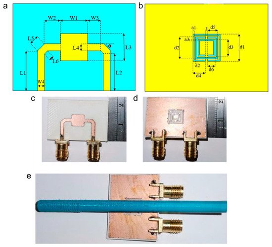
Carbon nanotube (CNT)-based SPR metastructures have also been reported where the Fano model was used to optimise the sensor performance. The device demonstrated a sensitivity of 1.38 × 10⁻²/ppm from 1–10 ppm and 3.0 × 10⁻³/ppm over 10 ppm [95][128]. Moreover, a metamaterial-based CSRR sensor was fabricated on Roger RO3035 substrate with a thickness of 0.75 mm, a relative permittivity of 3.5 and a loss tangent of 0.0015. To improve the sensitivity and Q factor, the chemical samples were introduced to a capillary glass tube placed in parallel to the sensor surface [96][129]. Figure 12a,b show the geometric features of the sensor and Figure 12c–e show the physical implementation. To distinguish branded diesel oil from unbranded oil, a MM-based sensor incorporating a microstrip transmission line was developed [97][130]. MM-based transmission line sensor has also been used to investigate the contamination of branded local spirit by methanol [98][131]. The sensor demonstrated a high sensitivity to detect methanol content with a bandwidth of 150 MHz. A highly sensitive SRR metastructure integrated with a PDMS microfluidic channel has been reported for glucose monitoring [99][132]. An interdigitated capacitor was utilised to intensify the E field, thereby improving the sensitivity over a wide range of glucose concentrations (i.e., 0 to 5000 mg/dL) [99][132].
Another interesting metamaterial-based chemical sensor was developed by incorporating multiple symmetrical double SRRs. Such a structure holds promise in multi-band sensing of chemicals [100][133]. The core feature of this sensor lies in a miniaturised, reusable, label-free and non-destructive metamaterial-microfluidic combination to determine the chemical property of liquids. Likewise, a phase change material derived from the Ge2Sb2Te5 (GST) combination was used to develop a temperature tuned sensor for detecting haemoglobin and urine [101][134].
Leitis et al. developed a novel germanium-based MS that adsorbed molecules over a broad spectrum from 1100 to 1800 cm−1 with a substantially high Q factor [102][135]. This novel structure combined angle-multiplexed refractometric sensing with the chemical specificity of infrared spectroscopy, thereby eliminating the need to use complex spectroscopic equipment or tunable light sources.
In recent years, metamaterial-based chemical sensing has drawn much attention in the MHz, GHz and THz, regimes [103][104][105][106][107][136,137,138,139,140]. Table 3 outlines some recently reported MM chemical sensors as well as a critical analysis of advantages of each sensor technology.
Table 3. Performance comparison of metamaterial-based chemical sensors.
| References | Advantages/Disadvantages | Target Analyte | Sensor Configuration | Sensitivity | Frequency (f)/Analyte Concentration Range/Limit of Detection (LOD) |
|---|---|---|---|---|---|
| [71][91] | |||||
| [ | |||||
| 103 | |||||
| ] | |||||
| (+) high sensitivity detection of scattered data | |||||
| (+) adequate penetration depth | Glucose | Copper pad on FR-4 substrate | 0.0125 dB/(mg/dL) | f range: 2.2 GHz to 3.8 GHz | Conc. range: 100–300 mg/dl |
| [114][104] | (+) Ultralow limit of detection | anti-BSA | Al coated periodic nanopillar arrays | 0.14 ng/mL | f range: 333 THz to 1000 THz Conc. range: 0.001–1000 ng/mL LOD: 1 pg/mL |
| [115][105] | (+) No pretreatment required | Vitamin D | Au coated cross and star shaped nanostructures on silicon substrate |
500–800 nm/RIU | LOD: 86 pM |