Your browser does not fully support modern features. Please upgrade for a smoother experience.
Please note this is a comparison between Version 1 by Alfrendo Satyanaga and Version 2 by Peter Tang.
Photoinduced processes governed by light activated TiO2 have been studied in many ways. One of the most active areas is the development of TiO2 photocatalysis technologies on their application for reducing environmental impacts. The immobilization of TiO2 on solid support, such as cementitious materials, greatly enhances its use in practical applications.
- photocatalysis
- cementitious materials
- titanium dioxide
1. Introduction
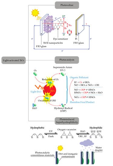
Photoinduced electron transfer (PET) is a key process in photocatalysis. Absorption of photon energy greater than the energy barrier of semiconductor materials could activate many chemical reactions [1][2][19,20]. Photovoltaic, photocatalysis, and photoinduced super hydrophilicity are the examples of photoinduced electron transfer. Although these processes could be utilized for many applications, these processes originate from a similar mechanism as shown in Figure 1. Semiconductors can absorb the light with energy greater than their bandgap and generate electron-hole pairs. The generated electron-hole pairs can be utilized for creating electric power (photovoltaic process), promoting chemical reaction (photocatalysis process), or altering its surface properties (super-hydrophilicity) [3][21]. The use of TiO2 for facilitating the photocatalytic reaction started decades ago and is becoming more important nowadays as indicated by the large number of publications [4][5][6][7][8][13,22,23,24,25]. One of the most active areas in the development of photocatalysis technologies is their application for photodegradation of pollutants.

Figure 1.
Applications of light-activated TiO
2
.
2. Semiconductor Photocatalysis
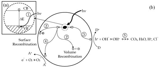
Figure 2 shows the primary steps in the photocatalysis mechanism. Photoinduced charge separation (step 1 in Figure 2a) followed by electron transfer process for redox reactions (step 3 and 4 in Figure 2b) are the key steps in the photocatalysis process. These steps will generate radicals that have the power to breakdown most of organic pollutant (step 5 in Figure 2b). In the absence of adsorbate, charge separation (step 1 in Figure 2a) will be followed by surface recombination or volume recombination (step 2 in Figure 2b). In this case, the photocatalysis process could not take place and the absorbed photon energy was released as heat.

Figure 2.
(
a
) Photoexcitation process; (
) Primary steps in photocatalytic mechanism. Reprinted with permission from Ref. [28] 2022, American Chemical Society.
In semiconductor, the valence band and the conduction band are separated by a bandgap ∆E, a region devoid of energy in a perfect crystal as shown in the enlarged section of Figure 2a. The highest energy band containing electrons is called the valence band (VB); the lowest empty band is called the conduction band (CB) [9][26]. The energy difference between the highest occupied band (the valence band), and the lowest unoccupied band (the conduction band) is called the bandgap, ΔE. By absorbing a photon energy equal to or greater than the band gap, ΔE, of the semiconductor, an electron is excited from the valence band into the conduction band, leaving behind a hole in the valence band (step 1), as shown in the enlarged section of Figure 2a [10][27]. The created electron-hole pair has a sufficient lifetime, in the nanosecond regime, to undergo charge transfer to adsorbed species on the semiconductor surface [11][28]. In the absence of the adsorbate, the excited electrons at the conduction band and holes at the valence band can recombine (step 2) and dissipate the input energy as heat.
If suitable, electron-hole scavengers, or surface defect state, is available to trap the electron or hole, and recombination is prevented and subsequent redox transfer may occur [10][27]. Photogenerated holes can be utilized to oxidize substrates at the semiconductor surface, as illustrated in step 3 of Figure 2b [12][29]. The holes trapped at the TiO2 surface can react with OH− to generate OH• radicals. The generated OH• radicals and holes themselves are a powerful oxidant. This powerful oxidant can degrade most of organic pollutant completely into a harmless final product (e.g., CO2 and H2O), as shown in step 5. In addition, the photoexcited electrons can react with electron acceptors adsorbed on the semiconductor surface (step 4). The reduction power of electrons can induce the reduction in molecular oxygen (O2) to form the superoxide anion (O2−). It has been confirmed that the superoxide is almost effective as holes and hydroxyl radicals in the chain reactions for breaking down the organic compounds [13][8]. Initiating an oxidation and reduction process at semiconductor surface is the principle of photodegradation [12][29]. Most organic photodegradation reactions utilize the oxidizing power of the holes either directly or indirectly [10][27]. During these processes, semiconductor remains intact and the charge transfer to the adsorbed species is continuous [11][28]. However, to prevent a build-up of charge, a reducible species should be provided to react with the electrons. In this system, photoinduced molecular transformations or reactions take place at the surface of a catalyst. The relevant photocatalytic processes may occur either at the air–solid interface or at the liquid–solid interface. Therefore, if the species are pre-adsorbed on the surface, the electron transfer processes could be more efficient.
3. Bandgap and Band Edge Position
As the recombination is an obviously destructive process for photocatalytic reaction, the efficiency of photocatalysis greatly relies on the competition between the electron transfer processes and recombination process [14][2]. The ability of a semiconductor to undergo photoinduced electron transfer to the adsorbed species is governed by the band energy levels of the semiconductor and the redox potential of the adsorbed species [11][28]. The band energy levels of the semiconductor and redox potential of the adsorbed molecule influence the photocatalytic process by controlling the charge transfer process of such surface photochemical reactions [12][15][3,29]. For that reason, knowing the band edge positions of semiconductors and redox potential of the adsorbate is useful for indicating the thermodynamic limitations for the photoreactions that can be carried out with the charge carriers [16][30].
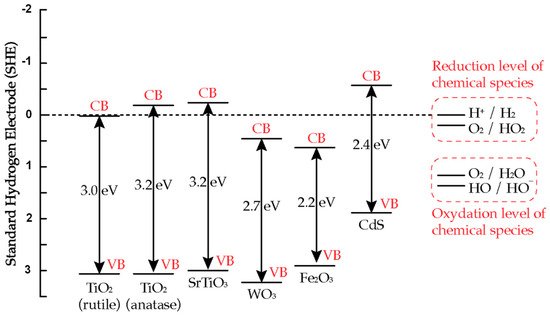
The band energy positions of several semiconductors is illustrated in Figure 3 [14][2]. In order to photo-reduce a chemical/adsorbed species, the conduction band position of the semiconductor has to be positioned above the relevant reduction level of the chemical species. In order to photo-oxidize a chemical species, the valence band position of the semiconductor has to be positioned below the relevant oxidation level of the chemical species. As illustrated in Figure 3, the bandgap of several semiconductor materials is in the range of 2.2–3.2 eV, corresponding to wavelength range from 564 to 388 nm. In photocatalysis, visible light photoactivation (>400 nm) is preferred by choosing low bandgap semiconductors. However, scientific investigations showed that the low bandgap semiconductors are subject to photocorrosion (oxidation of semiconductor) that results in loss of activity after a period of time [15][3]. In contrast, TiO2 has been found to be chemically stable and resistant to photocorrosion and yet highly photoactive [14][17][2,31].

Figure 3. Valence and conductance band positions for various semiconductors and relevant redox couples at pH 0 [14].
Valence and conductance band positions for various semiconductors and relevant redox couples at pH 0. Reprinted with permission from Ref. [2] 2022, Elsevier.
4. TiO2 Based Photocatalyst
TiO2 naturally occurs in three different types of crystal structure: anatase, rutile, and brookite [18][32]. Two of them, anatase and rutile, are commonly used in photocatalysis. As shown in Figure 3, the bandgap of anatase is 3.2 eV, while the bandgap energy for rutile is 3.0 eV, which is 0.2 eV narrower than anatase. Lower bandgap materials, such as rutile, should be preferred as they could absorb photon with smaller energy for photoactivation. However, in the literature, anatase shows higher photocatalytic activity than rutile under UV light irradiation. This is due to a more negative conduction band position of anatase than that of rutile (Figure 3), resulting in more reactive species formed [3][21].
The scientific concept of TiO2 photocatalysis was introduced by Fujishima and Honda [5][22]. They discovered the photocatalytic water splitting in a photo-electrochemical cell. Using TiO2 electrodes in a photo-electrochemical cell, water could be dissociated into its constituent parts, hydrogen and oxygen gases, under ultraviolet (UV) illumination. This discovery triggered much research in understanding the fundamental mechanism and in improving the efficiency of TiO2 photocatalyst. In recent years, one of the most active areas in the development of photocatalysis technologies is their application for environmental cleanup. However, due to wide bandgap of the TiO2 material, pure TiO2 photocatalyst can only be activated by UV irradiation [11][19][20][28,33,34]. While it can use natural sunlight-UV irradiation, sunlight only contains a small amount of UV photon that can be used to carry out reactions at the TiO2 surface. Therefore, one of the main challenges in improving the performance of TiO2 photocatalyst is to extend their optical response from UV to visible region.
Improving the optical response and photocatalytic performance of TiO2 in the visible light region can be achieved by doping or sensitization as shown in Figure 4 [21][35]. Doping is a kind of bulk chemical modification to alter the chemical composition of TiO2 but maintain the integrity of TiO2 crystal structure. This technique substitutes the metal (titanium) or the non-metal (oxygen) component in order to alter the optical properties of TiO2 nanomaterials. Figure 4b shows an example of metal doped, V-doped TiO2 [22][36]. V-doped TiO2 is the metal doping of TiO2 with vanadium (V) to shift the absorption spectra of TiO2 to a lower energy region (red shift) with the increase in the concentration of dopant. The red shift is attributed to the charge transfer transition between d-electron (t2g level) of the V dopant and the CB of TiO2. The bandgap of V-doped TiO2 is lower than pristine TiO2. Hence, it can be photoactivated by visible light irradiation.

Figure 4.
Improving optical response of (
a
) TiO
2
, (
b
) V-doped TiO
2
, (
c
) sensitization by narrow bad gap semiconductor.
An alternative technique is photosensitization, a photochemical process by which a chemical reaction is induced by energy transfer from the light-absorbing sensitizer [23][37]. As shown in Figure 4c, charge transfer from the excited sensitizer to conduction band of TiO2 is a key step in these processes. The match of energy difference between the oxidation potential of the excited sensitizer and conduction band of the TiO2 acts as the driving force for the charge injection process [24][38]. The sensitizer for TiO2 materials can be any materials with lower bandgap, including semiconductors, metals, and organic dyes.
