Thin Film Superconductors: Comparison
Please note this is a comparison between Version 2 by Beatrix Zheng and Version 1 by Sunday Oyinbo.

Thin superconducting films have been a significant part of superconductivity research for more than six decades. They have had a significant impact on the existing consensus on the microscopic and macroscopic nature of the superconducting state.  Thin-film superconductors are frequently considered to be Type II superconductors even when they are from Type I materials because of the strong effect of the stray magnetic fields outside the superconductive sample [28]. Thin films can be defined as materials, where one dimension is highly constrained relative to the other two dimensions or a system whose properties are determined by the surface energy. Thin films consist of two main components: the microstructure and the surface morphology. The microstructure refers to the microscopic crystal structure of the thin film. Thin films fabrication has a virtually unlimited ability to synthesise materials with new or improved properties. This means new devices and applications can be realiszed.

  • thin film superconductors
  • Meissner effect
  • atomic layer deposition
  • thin-film technology
  • pulsed laser deposition

1. Fe-Based Thin-Film Superconductors

High-Tc (Tc > 20 K) superconductivity in Fe-based superconductors [21,43][1][2] was discovered in 2008 by Watanabe et al. [44][3]. Epitaxial iron-based thin-film superconductors [45][4] of very high quality are crucial in the manufacture of iron-based superconducting gadgets, like the Josephson junctions [46][5] and superconducting quantum interference devices (SQUIDs) [18][6]. They are also utilised in emerging iron-based superconductive coated conductors with high critical current density (Jc) under powerful magnetic fields. Thin films are also needed for academic purposes to realise the intrinsic characteristics of iron-based superconductors as substantial bulk solitary crystals are not easy to grow for some iron-based superconductors. There are various families/groups in which iron-based superconductors can be put into. InHere this paper, we e researchers identify these families as, LnFeAs(O,F) (where the Ln is the lanthanide element), also called the 1111 group, doped AeFe2As2 (where Ae is an alkaline-earth element) also the termed 122 group, FeCh (where Ch is a chalcogen) also termed the 11 group, and the FeSe mono-layer film, also called the 11-mono layer group. Molecular beam epitaxy and pulsed laser deposition are the most common Fe-based thin film fabrication and growth mechanisms. Several thin-film synthesis and applications articles [43,47,48,49,50,51,52,53,54][2][7][8][9][10][11][12][13][14] for iron-based thin-film superconductors have been published.

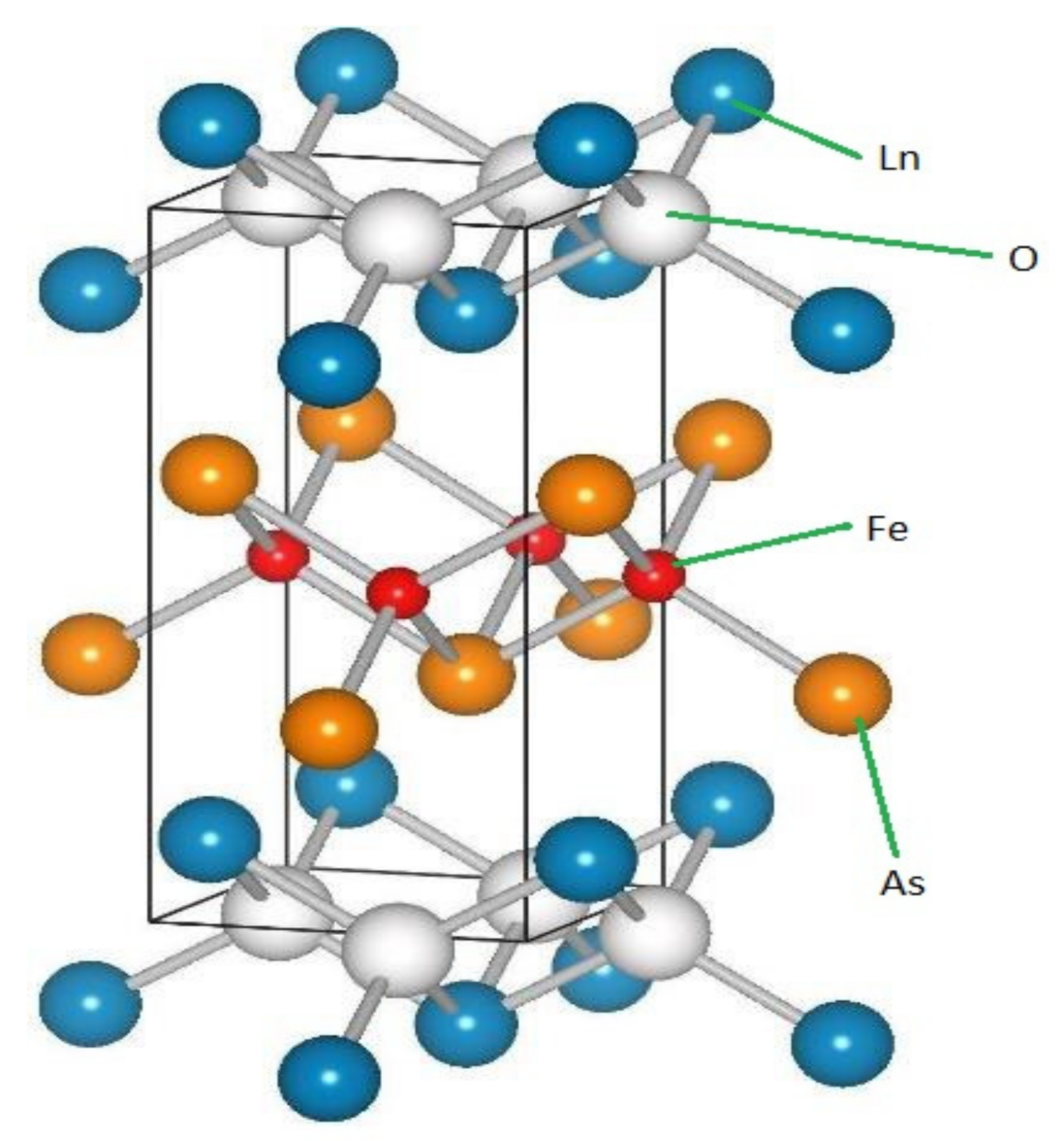
1.1. LnFeAs(O,F) Family
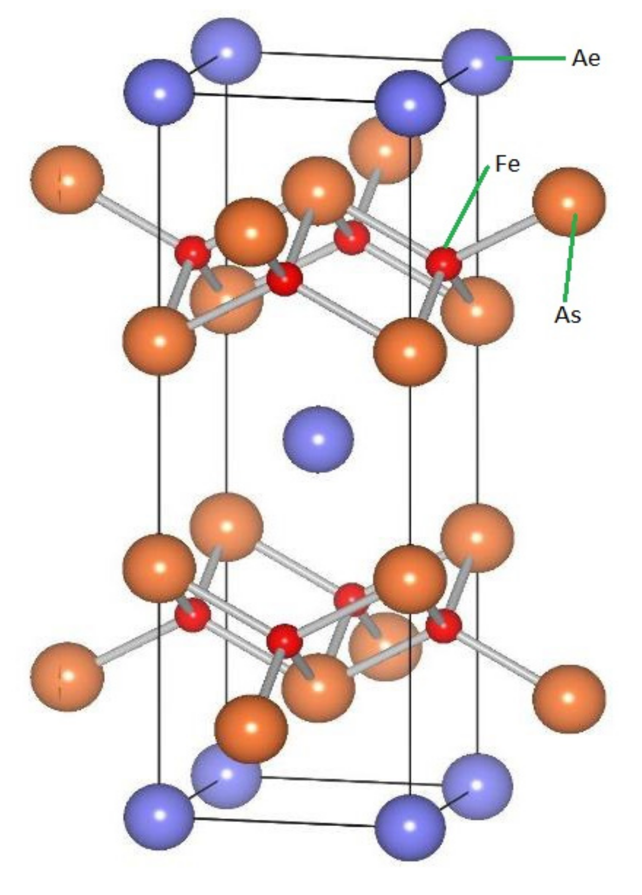
The first high-Tc iron-based superconductor to be discovered, with Tc 26 K, is LaFeAs(O,F). It was discovered by Kamihara et al. [24,55][15][16]. They also discovered low-temperature iron-based superconductors, including LaFePO, whose Tc is approximately 4K [56][17], LaNiPO whose Tc is approximately 3 K [26][18] and LaNiAsO whose Tc = 2.4 K [24][15]. These discoveries were made during the group’s investigation of transparent p-type oxychalcogenide semiconductors like LaCuSO [26][18]. The group managed to increase Tc to 55 K by replacement of a lanthanoid element (Ln) from Lanthanum to Neodymium [57][19]. The LnFeAs(O,F) family is called the “1111” group. The following Figure 41 shows the LnFeAsO microstructure.
Figure 41.
Ln
FeAsO structure.
The growth of LaFeAs(O,F) thin-films was first attempted by Hiramatsu et al. [47][7]. Several processes such as reactive solid-phase epitaxy and simple pulsed laser deposition (PLD) growth were attempted to deposit the thin superconducting films of LaFeAs(O,F). Solid-phase epitaxy had been previously successful in growing LaZnOPn, but failed to produce satisfactory growth of LaFeAs(O,F). The breakthrough of getting the epitaxial films of LaFeAsO was brought by the simple pulsed laser deposition process (PLD). The Nagoya group employed molecular beam epitaxy (MBE) [58,59][20][21] and advanced the thin film growth of the 1111 compounds.
Backen et al. [60][22] reported on the synthesis of LaFeAsO1−xFx superconducting film of polycrystalline by the ex-situ technique. They deposited the LaFeAsO1−xFx films on MgO and LaAlO3 substrates by a pulsed layer deposition method. Annealing was then done at elevated temperatures in an evacuated silica-glass tube to obtain the superconducting thin films. The thin film transitioned into a superconducting state at approximately 11 K. The superconducting thin films showing a zero resistivity around the critical temperature of bulk samples were positively synthesised by reviewing the annealing state [61][23].
Naito and Ueda et al. [62][24] reported on the SmFeAsO (Sm1111) thin film on CaF2 substrate synthesised by molecular beam epitaxy. The film transitioned into a superconducting state at around 56 K. This was somewhat higher than Tc of SmFeAs(O,F) bulk samples [59,62][21][24]. CaF2 was first used by Tsukada et al. [63][25] as a substrate in the deposition of FeSe1−xTex. CaF2 is effective in the manufacture of other iron-based superconductors, as evidenced by the enhancement of Tc in Sm1111 film [62][24].
Haindl et al. [64][26] grew superconductive Sm1111 films on CaF2 substrates using pulsed layer deposition. They noted that SmFeAs(O,F) films synthesised on BaFe2As2-buffered MgO substrates by employing the SmFeAsO0.9F0.1 polycrystalline target had virtually identical lattice parameters with those of SmFeAsO bulk samples. They, however, exhibited a glitch, alleged to be a result of structural transition [65][27], near a temperature of 150 K and no superconductivity in the temperature dependence of resistivity. These findings showed the insufficiency of the F content in this film. The Sm1111 film on CaF2 substrate fabricated from the identical target transitioned into a superconducting state at 40 K.

1.2. Doped AeFe

2

As

2

family

In the second group (doped AeFe2As2 or (Ae,K)Fe2As2), usually termed “122” compounds [66,67][28][29] the one with the highest Tc of ~38 K is Ba0.65K0.35Fe2As2. The compounds in this group have the crystal structure of ThCr2Si2 type. There is an alternating stacking of tetrahedron Fe2Pn2 layers and plain Ae layers in this family of compounds [21][1]. Pn is the pnictogen atom, it can either be As or Sb. Figure 52 shows the AeFe2As2 structure.
Figure 52.
Ae
Fe
2
As
2
structure. The alternating stack of tetrahedron Fe
2
Pn
2
layers and plain Ae layers can be seen in this structure.
Thin films of (Ae,K)Fe2As2 can be synthesised by using FeAs self-flux or Sn flux under ambient pressure. (Ae,K)Fe2As2 films growth is more difficult than LnFeAs(O,F) films. A group from Sungkyunkwan University synthesised superconductive (Ba,K)Fe2As2 films by a post-annealing method [68,69][30][31]. The TAT (Tokyo University of Agriculture and Technology) group synthesised thin films of (Ba,K)Fe2As2 and (Sr,K)Fe2As2 by molecular beam epitaxy [70,71,72,73][32][33][34][35]. Potassium is very volatile; therefore, it is not included in films grown at Ts > 400 °C. The TAT group worked on finding new superconductors and improving the Tc of Fe-based superconductors. Potassium-containing 122 films synthesis is performed at Ts ≤ 400 °C. The Fe-based superconductor Ba1−xKxFe2As2 is used as a key material for high magnetic field applications such as superconducting wires and bulk permanent magnets.

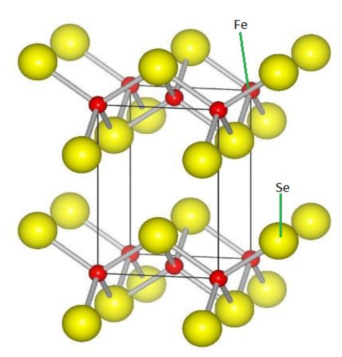
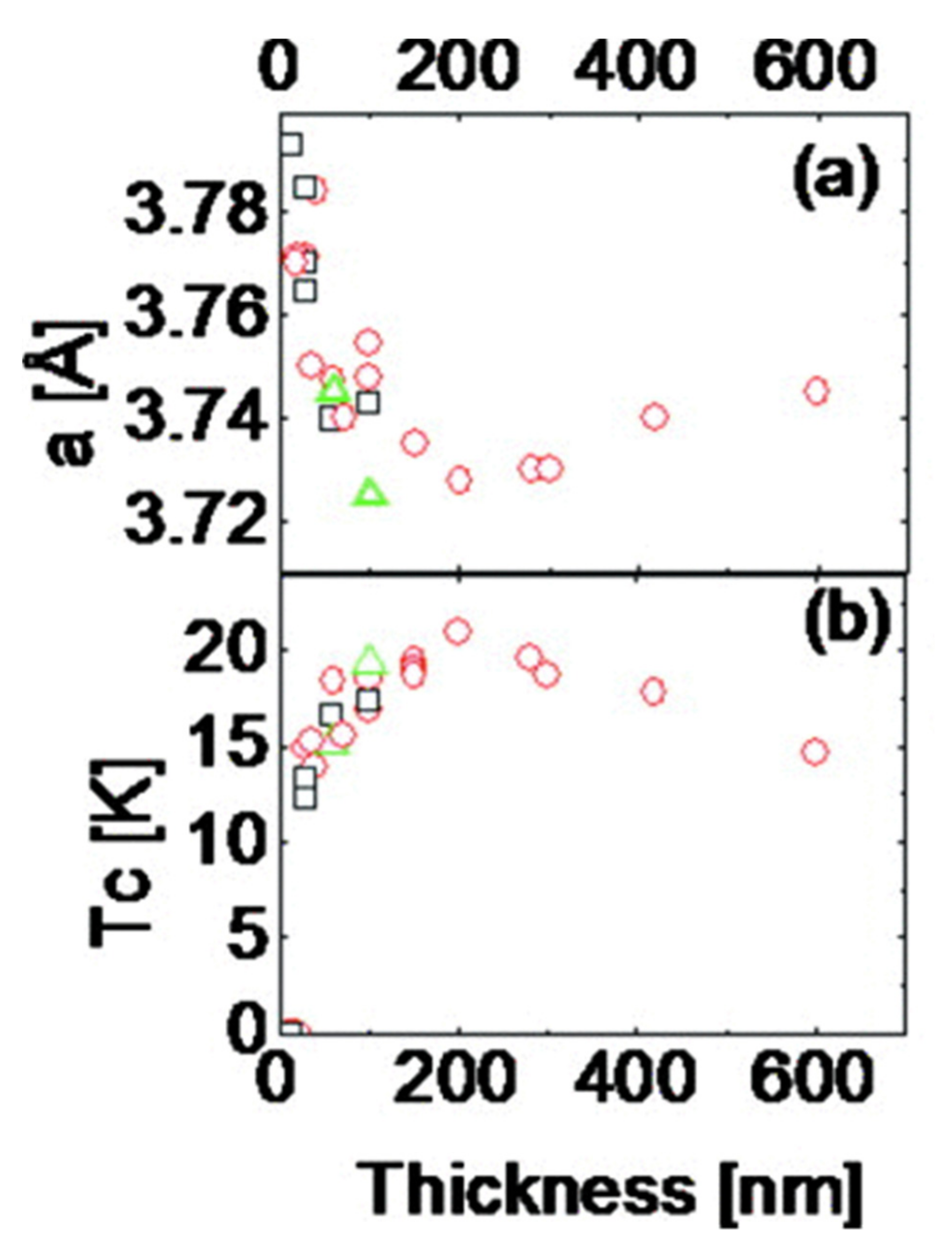
1.3. FeCh and FeSe Mono-Layer Film Family

In the family of FeCh, also called the 11 compounds, divalent chalcogen ions surround the divalent Fe ions tetrahedrally. FeCh structure is a sequential stacking of neutral tetrahedron Fe2Ch2 layer by van der Waals interaction. The Wu group [74][36] discovered the superconductivity in FeSe (whose Tc is approximately 8.5 K) [55,75][16][37] and FeSe0.5Te0.5 (whose Tc is approximately 14 K) [75][37] after the report on the unearthing of superconductivity in LaFeAs(O,F) by Hosono and his colleagues [53][13]. The critical temperature of FeSe can be increased significantly when hydrostatic pressure is applied. It reaches 37 K at around 10 GPa [76,77][38][39]. Figure 63 shows the structure of FeSe.
Figure 63.
FeSe structure. Reddish brown balls are Fe atoms, while yellowish balls represent Se atoms.
The synthesis of group “11” iron-based thin films has been slow due to their toxicity [21][1]. FeSe1−xTex thin films growth was first realised by Wu et al. [74][36] by a pulsed laser deposition technique. Bellingeri et al. [78][40] reported that Tc in FeSe0.5Te0.5 thin films could be increased up to 21 K from around 14 K by varying thickness. Figure 74 shows the thickness dependence of Tc that they reported.
Figure 74. Tc thickness dependence of FeSe0.5Te0.5 films. In (a) the thickness is plotted vs. lattice constant a [Å] while in (b) the thickness is plotted vs. Tc [K]. Structural analyses showed that the cfilm (=5.84–5.89 Å) is less than the bulk values (cbulk = 5.995 Å) though independent of the film thickness.
Hanzawa and his colleagues [79][41] synthesised FeSe films, which were 100 Å thick on SrTiO3 by molecular beam epitaxy. The highest Tc obtained was 35 K. Lei et al. [80][42] conducted comparable experiments employing the flux method to grow FeSe single crystals. Table 1 summarises some of the transition temperatures of superconduction of the FeSe and Fe(Se,Te) thin films synthesised by molecular beam epitaxy and pulsed layer deposition.
Wang and his group [82][44] detected large energy gaps that possessed superconducting properties using scanning tunnelling spectroscopy (STS) at low temperatures in mono-layer FeSe thin films on TiO2-terminated STO (perovskite SrTiO3) grown by molecular beam epitaxy. The U-shaped gap was found to have a magnitude of 40.2 meV at 4.2 K.

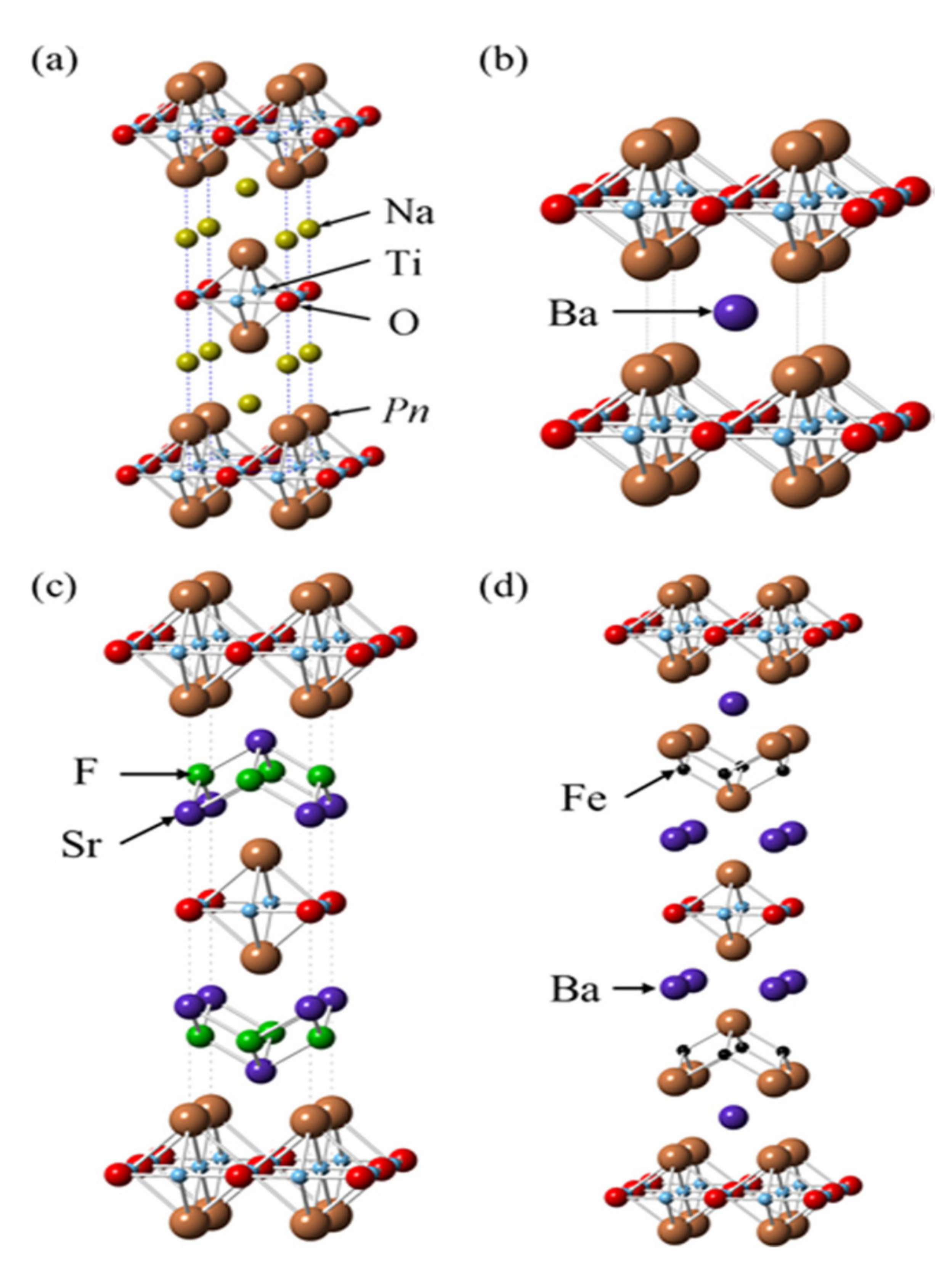
2. Layered Titanium Compounds

Layered titanium oxypnictides parent compounds are metallic without carrier doping, unlike cuprate superconductors [93,94,95][55][56][57]. Hosono et al. [48,49][8][9] prepared the BaTi2Sb2O compound in 2012 and detected a bulk transition into superconductivity at a temperature of 1 K [96][58]. Doan and his group [97][59] autonomously presented an improved Tc of 5.5K in BaTi2Sb2O when it was doped with Na. BaTi2Sb2O was prepared via the solid-state reaction technique using very pure BaO, Ti, and Sb according to their stoichiometric ratios [96][58]. This involved wrapping the specimen in a tantalum foil, sealing in a quartz tube and heating for a period of 40 h at an elevated temperature of 1000 °C. The sample was then cooled at a rate of 50 °C per hour up until room temperature was reached. The resulting compound had a tetragonal structure. X-ray diffraction and neutron diffraction data was used to determine the crystal structure of BaTi2Sb2O. It showed that the crystal structure is the same as that of BaTi2As2O [98][60]. Figure 85 shows the various crystal structures of layered titanium compounds. The Tc of BaTi2Sb2O was found to be 1.36 K. Figure 96 shows the synchrotron X-ray diffraction refinement results for BaTi2Sb2O and BaTi2Bi2O with the P4/mmm space group.
Figure 85.
Crystal structures of different layered titanium compounds (
a
) Na
2
Ti
2
Pn
2
O, (
b
) BaTi
2
Pn
2
O, (
c
) (SrF)
2
Ti
2
Pn
2
O, and (
d
) (Ba
2
Fe
2
As
2
)Ti
2
As
2O [54]. Pn is either Sb or As.
O [14]. Pn is either Sb or As.
Figure 96.
Refined synchrotron x-ray patterns of (
a
) BaTi
2
Sb
2
O and (
b
) BaTi
2
Bi
2O. The Bragg reflection positions are shown by the green ticks [54].
O. The Bragg reflection positions are shown by the green ticks [14].
The Ti pnictide oxides BaTi2Pn2O (where Pn is Sb or Bi) contain layers of superconductive Ti2Pn2O and Barium blocking layers [98][60]. Several titanium pnictide oxides have been produced. These include Na2Ti2Pn2O (where Pn is As or Sb), (SrF)2Ti2Pn2O (where Pn is As, Sb, or Bi), and BaTi2Pn2O (where Pn is As, Sb, or Bi). Amongst these compounds, only BaTi2Pn2O (where Pn is Sb or Bi) shows superconductive characteristics [96,97,99,100,101,102][58][59][61][62][63][64]. BaTi2Sb2O and BaTi2Bi2O were manufactured using the conventional solid-state reaction [96,98][58][60]. BaTi2Bi2O is unstable in air and some solvents, as it easily decomposes when exposed to air forming Bi-based phases such as BaBi3 and Bi. Figure 107 shows the resistivity and magnetic susceptibility of BaTi2As2O. The electronic structure of a compound is vital in understanding its superconductivity. The BaTi2Sb2O electronic structure as reported by Singh [103][65] from first principles calculation showed that three d orbitals dxy, dx2−y2, and dz2 have a substantial contribution at the Fermi level. This indicates that BaTi2Sb2O has a multiband nature. The oxygen 2p and Antimony (Sb) 5p are filled, while the Antimony 5p are hybridised with Titanium 3d. No Ba-derived occupied valence bands are present. The formal valence shown by the results is Ba2+Ti3+Sb3−O2−. The one 3d electron of Ti is responsible for the transport and magnetic characteristics of the composite [95][57]. In the BaTi2Bi2O electronic structure, as reported by Suetin and Ivanovskii [104][66], the three d orbitals have a substantial contribution at the Fermi level as is the case with BaTi2Sb2O.
Figure 107.
(
a
) The resistivity curve and (
b
) magnetic characteristics of BaTi
2
As
2
O. The low-temperature enlarged scale magnetic field effect is shown by the inset in (
a) [54].
) [14].

3. Intercalation Compounds with Layered and Cage-like Structures

Examples of high-temperature superconductors with layered or cage-like structures are cuprates [105[67][68],106], iron pnictides [24[3][15][69],44,107], MgB2 [51,108,109][11][70][71] and alkali metal-doped fullerides [54][14]. Their intercalated structures are made of charged (doped) layers attached to charge basins in the interlayer/cage-like space. There are two sub-families of layered polymorphs in metal nitride halides: the α-form and β-forms with stoichiometric formula MNX (where M is Ti, Zr, or Hf, N is Nitrogen and X is Cl, Br, or I). The α-form is an orthogonally MN layered network divided by halogen atoms, while the β-form contains dual honeycomb-like MN layers squeezed in between compact halogen layers [110,111][72][73]. MNX compounds are prepared by reacting the metal or metal hydride with ammonium halides at elevated temperatures [112][74]. The chemical reaction is:
M   o r   M H 2 + N H 4 X   M N X + 2   o r   3 H 2 .
MNX compound was then ferried in a quartz glass tube with a little amount of NH4X using a furnace whose temperature was between 750 and 850 °C. The resulting compounds were of α-form. The β-form was obtained by subjecting the α-form to a pressure of between 3 and 5 GPa at a temperature of around 800 °C. These superconductors have no magnetic ions, hence a magnetic pairing mechanism is not considered, but the possible candidates for the pairing mechanism have been assumed to be charge and spin fluctuations [113,114,115][75][76][77]. Figure 118 shows the α- and β-form structures of the metal nitride halides.
Figure 118. Crystal structures of the α-form and the β-form of (where M is Ti, Zr, or Hf and X is Cl, Br, or I). The red atoms represent the metal (M) atoms; the blue are the Nitrogen atoms, and the green are halogen atoms (X).
When β-HfNCl is doped by intercalation of alkali metals, a high-temperature superconductor (Tc > 20 K) is obtained [54][14]. Yamanaka et al. [116][78] detected the highest Tc value of 25.5 K in the lithium and tetrahydrofuran (THF) co-intercalated superconductor Li0.48(THF)yHfNCl. Earlier, Yamanaka et al. [117][79] found Zr homologue LixZrNCl to exhibit superconductive characteristics at Tc of approximately 14K. α-TiNCl required electron doping with alkali metals and organic bases like pyridine and alkylene diamines to be transformed into a superconductor [54][14]. Magnetic susceptibility was conducted on the Lithium intercalated sample, Li0.56HfNBr, from the chemical reaction with n-BuLi in hexane. The following Figure 129 shows the temperature dependence of the magnetic susceptibility of Li0.56HfNBr.
Figure 129. Temperature dependence of the magnetic susceptibility of Li0.56HfNBr. χ = C/(T − ϴ) + χ0. C is the curie constant and has the value of 0.0145(1) emu K mol−1, ϴ = 0.04(2) K and χ0 = 0.00126(1) emu mol−1.
There are also silicon clathrates and related compounds that have cage-like structures. High pressure and high temperature (HPHT) conditions can be used to prepare the Ba-containing silicon clathrate compound Ba8Si46. The compound displays superconductivity at Tc = 8.0 K [110][72]. HPHT application is favourable for synthesising binary phases that are rich in Si such as LaSi5, LaSi10, BaSi6, Ba24Si100, Ba8Si46, NaSi6, Na8Si46, and NaxSi136 [54,110,118,119,120][14][72][80][81][82]. Tanaka et al. [121][83] synthesised Ca2Al3Si4 using the HPHT method. The compound showed superconductive transition at Tc = 6.4 K.

4. Other Superconductors

In this group, wthe researchers discuss the superconducting compounds that fall outside the previous categories already mentioned. These compounds fall into the low-temperature and high-temperature superconductors.
AM2X2-type (where M is not Fe) superconductors are an example of 122-type superconductors. Some non-Fe 122-superconductors have the ThCr2Si2-type structure and include compounds such as SrNi2P2 [122][84], BaNi2P2 [107][69], BaRh2P2, BaIr2P2 [123][85], LaRu2P2 [124][86], LiCu2P2 [125][87], SrNi2As2 [126][88], and BaNi2As2 [127][89]. An example of 122-type antimonides and associated compounds is SrPt2Sb2 [128][90]. Its measurements of electrical resistivity, magnetisation, and specific heat indicated a transition into superconductivity at Tc = 2.1 K. The compound was manufactured by Hosono et al. [54][14] in two steps; arc melting and remelting of the specimen starting from Sr, Pt, and Sb. The superconductor is of Type II and has a lower critical field (Hc1) and upper critical field (Hc2) of 6 Oe and 1 kOe, respectively, at a temperature of 1.8 K [54][14].
Cobalt-based superconductor LaCo2B2 [129][91] was synthesised using the arc-melting technique for Lanthanum, Cobalt, Boron, Yttrium, and Iron mixtures. It was found to be superconductive after constituent cation isovalent or aliovalent substitution [54][14]. Density Functional Theory (DFT) was used to investigate the electronic structure of LaCo2B2. From these calculations, it was confirmed that La ions take +3 state. It was also confirmed that the strong covalent CoB layer is responsible for metallic conduction. Pauli paramagnetic state results due to the suppression of the spin moment of the Co ion by this strong covalency [54][14]. Figure 130 below shows the calculated Density of State (DOS) of the LaCo2B2 compound.
Figure 130.
Calculated density of state (DOS) of LaCo
2
B
2
.
BaNi2As2 has a tetragonal ThCr2Si2 type crystal structure at room temperature [127,130,131][89][92][93] and undertakes a transition of its structure at approximately 130 K to a triclinic structure where alternate Nickel-Nickel bonds are created in the Nickel plane. This new phase shows conventional BCS type superconductive characteristics below 0.7 K [127,131,132,133][89][93][94][95]. The BCS type superconductivity is based on the formation of Cooper pairs. The electron-electron interaction that results from virtual exchange of phonons is non-repulsive when the energy difference between the electrons states concerned is below the phonon energy. During pair formation, two electrons with opposite spin always combine with each other [22][96]. One electron creates a positive charge fluctuation, which then attracts a second incoming electron behind it. This attraction continues creating a train of electrons. In the superconducting state, the two electrons interact via a phonon or lattice distortion forming a cooper pair. BaNi2As2 superconductivity can be enhanced through phosphorus doping, the transition temperature, which is lower than 0.7 K for the triclinic phase with x less than 0.07, is increased to 3.33 K in the tetragonal phase with x = 0.077. Hosono et al. [54][14] grew single crystals of BaNi2(As1−xPx)2 by a self-flux method using mixtures of Ba, NiAs, Ni, and P. Figure 114 shows the temperature dependence of electrical resistivity parallel to the ab plane. ρab was normalised by the value at 300 K for BaNi2(As1−xPx)2. Phosphorus doping suppresses the triclinic phase, leading to the improvement of superconductivity. Figure 152 shows the BaNi2(As1−xPx)2 system phase diagram.
Figure 114. Temperature dependence of electrical resistivity parallel to the ab plane for BaNi2(As1−xPx)2 crystal. The resistivity arnomally shown by thermal hysterisis in the figure shows tetragonal to triclinic transition [134][97].
Figure 152. BaNi2(As1−xPx)2 system electronic phase diagram [134][97]. SC1 and SC2 shows the phases of superconduction. Tetragonal-to-triclinic structural transition temperatures (Ts) upon cooling and heating are shown by open and closed diamonds, respectively. Ni planes in the triclinic and tetragonal phase are shown by the inserts.
Transition metal dichalcogenides MX2 have two families; CdI2-type telluride family and the pyrite (FeS2)-type chalcogenide family [54][14]. Self-flux technique was used to grow crystals of IrTe2 [135][98]. This involved mixing powders of Ir and Te at a ratio of 18:82 and placing it in a sealed alumina crucible and then placing it into a bigger quartz tube. After evacuating and sealing, the contents of the tube were heated to a temperature of around 1223 K for a period of 10 h, then increased again to 1433 K. The next step was to cool to 1173 K at a rate of between 1 and 2 K per hour. The final step was to quench the quartz tube in ice. At a temperature of around 250 K, IrTe2 undergoes a transformation to a low temperature phase. The orbital degree of freedom is attributed to this transition since the Ir atoms’ d-orbitals are partially filled. Limited replacement of Platinum for Iridium in IrTe2 overwhelms the creation of the low-temperature phase, ensuing the superconductivity incidence [136,137][99][100]. Its superconductivity appears for approximately 0.04 < x < 0.14 in Ir1−xPtxTe2. The highest Tc of approximately 3.2 K is obtained at the trigonal and triclinic phase boundary when the x value is 0.04. When platinum is substituted, the Fermi level is shifted upwards. This affects the density of state near the Fermi level. The density of state is increased in the triclinic phase and decreased in the trigonal phase. The triclinic phase is also suppressed through the breakdown of the Ir-Ir dimers. Figure 163 shows the crystal structure of IrTe2 at different temperatures.
Figure 163. (a,b) The different views of the IrTe2 crystal structure at 300 K. The trigonal lattice unit cell is shown by the black lines. (c,d) The IrTe2 crystal structure at a temperature of 20 K. The blue and black lines show the triclinic lattice unit cell and the 5a × b × 5c supercell, respectively [135][98], where a, b, and c are the high-temperature trigonal-cell parameters.
Figure 174 shows the computed orbital-decomposed partial density of state for the high-temperature trigonal phase and the low-temperature triclinic phase of IrTe2. Ir2 dimers formation in the low-temperature phase yields strong bonding-antibonding splitting in the dyz bands of the two Ir3 atoms. This makes the energy of the antibonding bands to increase above the Fermi level and reduces the energy of the bonding bands by 1 eV [135][98].
Figure 174. The computed orbital-decomposed partial density of state for (a) the high-temperature trigonal phase and the (bd) low-temperature triclinic phase of IrTe2. The dotted line is the Fermi level [135][98].
An example of the chalcogenide family of pyrite-type is Ir dichalcogenides IrxCh2 (where Ch is Se or Te). The unit cell comprises of four Ir and eight Ch sites. The Iridium sites with haphazardly distributed vacancies make a simple fcc (face-centred-cubic) lattice structure. At times it assumes the pyrite-type structures when the Iridium site vacancies are introduced [138][101]. High-pressure application effectively stabilises the pyrite-type form against the Cd2I2- type one [139][102]. Qi et al. [140][103] employed high-pressure synthesis technique to synthesise pyrite-type IrxCh2 where the x value was near 1 and had transition temperature values of 6.4K and 4.7K for the two compounds Ir0,91Se2 and Ir0,93Te2, respectively. The density functional theory Qi et al. performed revealed that the compound consists of antibonding σ orbitals of the Se-Se dimer and dz2 orbitals of the Ir. This meant that the transition from nonmetal to metal and the transition from metal to superconductor are driven by relaxation due to bond lengths which are alternating in the Se dimers array. Figure 185 shows the pyrite structure of IrxSe2.
Figure 185.
Crystal structure of pyrite Ir
x
Se
2
. The reddish-brown atoms are Ir, while the cyan colour represents Se atoms.
A noncentrosymmetric superconducting system [141,142,143][104][105][106] contains a mixture of singlet and triplet states, called a mixed parity state. CePt3Si [144][107], CeCoGe3 [145][108], CeIrSi3, and CeRhSi3 [146][109] are examples of this superconductor class. The last three superconductors have a BaNiSn3-type structure.
Many silicide superconductors are noncentrosymmetric, and most of them crystallise and show conventional s-wave superconductivity. The exclusions are the Cerium containing heavy-fermion compounds. Hosono et al. [54][14] reported on two noncentrosymmetric silicide superconductors: SrAuSi3 [147][110] and Li2IrSi3 [148][111]. SrAuSi3 was the first noncentrosymmetric superconductor containing gold. Gold is a heavy element that causes strong spin-orbit coupling. The stability of the SrAuSi3 superconductor was found only under high pressure [147][110]. Figure 196 shows the crystal structure of SrAuSi3. The green atoms are Sr, blue are Si atoms, and gold atoms represent Au. SrAuSi3 is a relatively powerful coupling superconductor. Its Tc was approximated by the McMillan formula [149[112][113][114],150,151], using the standard value of 0.13 for the Coulomb repulsion parameter μ*, resulting in a value of ∼19 K. SrAuSi3 samples were synthesised using a high-pressure synthesis method at 6 GPa. The reactant powders of SrSi2, Au, and Si were mixed in equal ratios in an agate mortar and then pressed into a disc which measured 6.9 mm in diameter, 3 mm in thickness, and weighed around 500 mg. The pellet was then placed in cell of high pressure (6 GPa), heated, and the temperature was kept at 1500 °C (1773 K) for an hour. Quenching to room temperature within a few seconds then followed.
Figure 196.
Crystal structure of SrAuSi
3 [147]. The structure is closely related to the ThCr
[110]. The structure is closely related to the ThCr
2
Si
2
type and CaBe
2
Ge
2
type structures.
Figure 2017 illustrates the temperature reliance of resistivity quantified by fluctuating the magnetic field. The Tc of SrAuSi3 at zero magnetic field is 1.6 K. As the magnetic field increases, Tc decreases. It gives Hc2(0), which is approximately 2.2 kOe. This value is way lower than the Pauli limit (Hp(0) of 30 kOe). Hosono et al. [54][14] explain that the orbital pair breaking mechanism governs Hc2. There are several other non-Fe superconductors that have been reported, such as NbSiAs (Tc = 8.2 K) [152][115], CeNi0.8Bi2 (Tc = 4 K) [153][116], LaNiBN (Tc = 4.1 K), LaPtBN (Tc = 6.7 K), La3Ni2B2N3 (Tc = 15 K), La2Sb (Tc = 5.3 K) [153][116], Ban+2Ir4nGe12n+4 (Tc = 6.1 K for n = 1; Tc = 3.2 K for n = 2) [154][117], Nb4NiSi (Tc = 7.7 K) [155][118], Ti2O3 [156][119], and Ca2InN (Tc = 0.6 K) [157][120].
Figure 2017. Illustration of the temperature reliance of resistivity quantified by fluctuating the magnetic field. (a) The Tc of SrAuSi3 at zero magnetic field is 1.6 K. (b) As the magnetic field increases, Tc decreases. (a) is taken over a wide temperature range while (b) is on a narrow temperature range [54][14].
Cuprates are another group of other thin film superconductors that the weresearchers will discuss in this review. The cuprate superconductors can be fabricated by pulsed laser deposition (PLD), laser ablation and dc magnetron sputtering.
In 2017, Arpaia et al. [158][121] reported on the fabrication of ultrathinYBa2Cu3O7−δ (YBCO) films on a magnesium oxide substrate using the PLD technique from thicknesses ranging between 50 and 3 nm. Their deposition conditions were a temperature of 760 °C and an oxygen pressure of 0.7 mbar. After the deposition process, the deposited material was cooled at a rate of 5 °C/min. The group used atomic force microscopy (AFM) to perform morphological and structural characterisation. Scanning electron microscopy (SEM) and x-ray diffraction (XRD) were utilised to determine the film quality and structural properties, respectively. The team reported that the onset temperature of the superconducting transition slightly changes with the thickness of the film, while the zero-resistance temperature significantly decreases when reducing the film thickness. The lower onset transition temperature was attributed to both an increase and a decrease in oxygen doping in the film. Figure 218 shows the temperature versus resistance curve of YBCO thin films where the thickness values are 10, 20, and 50 nm.
Figure 218. Resistance vs. temperature curve of YBCO thin films where the thickness values are 10, 20, and 50 nm. The insert table shows the values of the calculated onset transition temperature for the three thicknesses. The insert on the right shows the temperature versus resistance measurement of an optically doped 50 nm bare thin film whose onset transition temperature was 89.1 K [158][121].
Stepantsov et al. [159][122] reported on the growth of superconductive YBa2Cu3O7−x thin films of b orientation on the surface of a SrLaGaO4 crystal using the Czochralski technique. The team deposited a buffer layer of PrBa2Cu3O7−x of 60 nm thickness onto the substrate surface using the rf sputtering technique. The chamber was filled with oxygen and argon gas mixture in a ratio of 1 to 4 up to a pressure of 0.1 mbars. The temperature of the substrate was raised to 600–750 °C while a 50 W rf discharge was applied between the target and the substrate. The chamber was then filled with pure oxygen to a pressure of 600 mbars and the substrate with the deposited film was annealed at 550 °C for an hour, after that it was cooled to room temperature. The chamber was then evacuated and replaced with a PLD chamber where the YBa2Cu3O7−x was grown. The team reported that the film is free of any other domains of crystallographic orientations of the intrinsic material, which includes the a-oriented component. Figure 2219 shows the resistance vs. temperature curve for YBa2Cu3O7−x.
Figure 2219.
Resistance vs. temperature curve of a b-oriented YBa
2
Cu
3
O
7−x
film grown on a substrate of SrLaGaO
4
.
Stepantsov et al. [160][123] reported on the fabrication of superconductive YBa2Cu3O7 thin-films with tilt CuO [100][62] planes to the surface on SrTiO3 substrate, using the pulsed laser deposition technique. The SrTiO3 single crystals, which were prepared by the Verneuil technique, were x-ray oriented, cut, and polished by a chemical-mechanical method to obtain substrates with one of the [100][62]—type planes tilted to the surface by 0 to 70° in 5° increments. YBa2Cu3O7 was then grown on these substrates by PLD. The team used the four circle Philips X’Pert Xray diffractometer to study the structure of the films. They found that YBa2Cu3O7 (YBCO) grown on the SrTiO3 was a single crystal with the (014) face oriented parallel to the surface. They also reported that YBa2Cu3O7 thin-films with CuO planes tilted to the surface by up to 41° can be deposited on the SrTiO3 crystal surface [160][123].
Kislinskii et al. [161][124] reported on the production of direct current superconducting quantum interference devices (dc SQUIDS) and Josephson junctions using YBa2Cu3O7 thin-films, which were deposited on ZrO2 bi-crystal substrates stabilised by yttrium, using laser ablation and dc magnetron sputtering. The team used a strip with a width of 30 µm to measure critical transition temperature and critical density of the films. The strip had been patterned by chemical etching. The deposited thin films had a Tc of 90 K and critical current density of approximately 2 × 10⁶ A/cm2. The voltage modulation depth of this SQUID was 6 µV. Figure 230 shows the voltage–current characteristic curves for the yttrium stabilised ZrO2 and YBCO.
Figure 230. (Left) I–V characteristics of the Josephson junction on the 28° misoriented yttrium stabilised ZrO2 bi-crystal without (represented by solid line) and with microwave radiation of 23.4 GHz (represented by broken line) at a temperature of 77 K. (Right) I–V curves for the 28° misoriented weak link of YBCO at different levels of 23.4 GHz microwave power (dotted lines) and without radiation (solid line) at 62 K.
Carillo et al. [162][125] reported on the resistance magneto-fluctuation measurements and proximity-effect in Nd1.2Ba1.8Cu3Oz (NBCO) to analyse the coherent charge transport in the non-superconducting state. The team discovered an unanticipated inhibition of Cooper pair transport, and the disappearance of superconductivity when the temperature was lowered from 6 K to 250 mK. Their magnetoconductance and conductance measurements pointed to the mechanism of pair breaking at temperatures lower than 2 K. In their investigation, the team showed a transition of an underdoped NBCO nanostructure from a temperature above 2–3 K where Cooper pair transport is permitted, to a lower temperature where the Cooper pairs are not permitted to flow.
Chaix et al. [163][126] reported on dispersive charge density wave excitations in Bi2Sr2CaCu2O8+δ. The team A new charge density wave (CDW) modulation was unearthed in underdoped Bi2.2Sr1.8Ca0.8Dy0.2Cu2O8+δ using ultrahigh resolution resonant inelastic X-ray scattering. Dispersive excitations were observed from an incommensurate charge density wave at low temperatures, which the enhanced phonon intensity. The CDW persisted near the pseudogap temperature, but other excitations drastically weakened, signalling a charge density wavevector shift. The phonon anomaly, dispersive CDW excitations and CDW wavevector analysis provided a momentum-space understanding of complex CDW behaviour. Figure 241 shows the temperature dependence of the charge density wave and the phonon anomaly.
Figure 241. Temperature dependence of the charge density wave and the phonon anomaly. (a) RIXS intensity map taken at a temperature of 240 K. The quasi-elastic region (centred at zero energy loss) and the phonon energy region (centred at 60 meV) used for computing the mean intensity profile shown in (b,c) are defined by the white dashed line. (b) Averaged intensity of the quasi-elastic region (indicated in (a)) at 240 K (red) and 20 K (blue). The dashed lines indicate the position of the charge density wave. (c) Mean phonon energy regions intensity as defined in (a), at 240 K and 20 K. The black arrow highlights the intensity anomaly at 20 K. Error bars in (b,c) are estimated by the noise level of the spectra. (d) Raw energy-loss spectra (markers) and the corresponding fits (solid lines) of RIXS data taken at T = 240 K (at the top) and T = 20 K (at the bottom). Filled areas highlight elastic peak fits. Red and blue boxes for T = 240 K and T = 20 K, respectively, represent the RIXS spectra where the elastic peak intensity is maximal (that is, the CDW position).

References

  1. Sakoda, M.; Iida, K.; Naito, M. Recent progress in thin-film growth of Fe-based superconductors: Superior superconductivity achieved by thin films. Supercond. Sci. Technol. 2018, 31, 093001.
  2. Imai, Y.; Nabeshima, F.; Maeda, A. Comparative Review on Thin Film Growth of Iron-Based Superconductors. Condens. Matter 2017, 2, 25.
  3. Kamihara, Y.; Watanabe, T.; Hirano, M.; Hosono, H. Iron-Based Layered Superconductor LaFeAs (x = 0.05 − 0.12) with Tc = 26 K. J. Am. Chem. Soc. 2008, 130, 3296–3297.
  4. Iida, K.; Hänisch, J.; Tarantini, C. Fe-based superconducting thin films on metallic substrates: Growth, characteristics, and relevant properties. Appl. Phys. Rev. 2018, 5, 031304.
  5. Virtanen, P.; Braggio, A.; Giazotto, F. Superconducting size effect in thin films under electric field: Mean-field self-consistent model. Phys. Rev. B 2019, 100, 224506.
  6. Antoine, C.Z.; Berry, S.; Bouat, S.; Jacquot, J.-F.; Villégier, J.-C.; Lamura, G.; Gurevich, A. Characterization of superconducting nanometric multilayer samples for superconducting rf applications: First evidence of magnetic screening effect. Phys. Rev. Spéc. Top. Accel. Beams 2010, 13, 121001.
  7. Hiramatsu, H.; Kamiya, T.; Hirano, M.; Hosono, H. Heteroepitaxial film growth of layered compounds with the ZrCuSiAs-type and ThCr2Si2-type structures: From Cu-based semiconductors to Fe-based superconductors. Phys. C Supercond. 2009, 469, 657–666.
  8. Hiramatsu, H.; Katase, T.; Kamiya, T.; Hosono, H. Thin Film Growth and Device Fabrication of Iron-Based Superconductors. J. Phys. Soc. Jpn. 2012, 81, 1–25.
  9. Tanabe, K.; Hosono, H. Frontiers of Research on Iron-Based Superconductors toward Their Application. Jpn. J. Appl. Phys. 2011, 51, 10005.
  10. Mele, P. Superconducting properties of iron chalcogenide thin films. Sci. Technol. Adv. Mater. 2012, 13, 054301.
  11. Haindl, S.; Kidszun, M.; Oswald, S.; Hess, C.; Büchner, B.; Kölling, S.; Wilde, L.; Thersleff, T.; Yurchenko, V.V.; Jourdan, M.; et al. Thin film growth of Fe-based superconductors: From fundamental properties to functional devices. A comparative review. Rep. Prog. Phys. 2014, 77, 046502.
  12. Sadovskii, M.V. High-temperature superconductivity in monolayers FeSe. Uspekhi Fiz. Nauk 2016, 186, 1035–1057.
  13. Hosono, H.; Yamamoto, A.; Hiramatsu, H.; Ma, Y. Recent advances in iron-based superconductors toward applications. Mater. Today 2018, 21, 278–302.
  14. Hosono, H.; Tanabe, K.; Takayama-Muromachi, E.; Kageyama, H.; Yamanaka, S.; Kumakura, H.; Nohara, M.; Hiramatsu, H.; Fujitsu, S. Exploration of new superconductors and functional materials, and fabrication of superconducting tapes and wires of iron pnictides. Sci. Technol. Adv. Mater. 2015, 16, 033503.
  15. Watanabe, T.; Yanagi, H.; Kamihara, Y.; Kamiya, T.; Hirano, M.; Hosono, H. Nickel-based layered superconductor, LaNiOAs. J. Solid State Chem. 2008, 181, 2117–2120.
  16. Hsu, F.-C.; Luo, J.-Y.; Yeh, K.-W.; Chen, T.-K.; Huang, T.-W.; Wu, P.M.; Lee, Y.-C.; Huang, Y.-L.; Chu, Y.-Y.; Yan, D.-C.; et al. Superconductivity in the PbO-type structure α-FeSe. Proc. Natl. Acad. Sci. USA 2008, 105, 14262–14264.
  17. Kamihara, Y.; Hiramatsu, H.; Hirano, M.; Kawamura, R.; Yanagi, H.; Kamiya, T.; Hosono, H. Iron-Based Layered Superconductor: LaOFeP. J. Am. Chem. Soc. 2006, 128, 10012–10013.
  18. Watanabe, T.; Yanagi, H.; Kamiya, T.; Kamihara, Y.; Hiramatsu, H.; Hirano, M.; Hosono, H. Nickel-Based Oxyphosphide Superconductor with a Layered Crystal Structure, LaNiOP. Inorg. Chem. 2007, 46, 7719–7721.
  19. Ren, Z.-A.; Che, G.-C.; Dong, X.-L.; Yang, J.; Lu, W.; Yi, W.; Shen, X.-L.; Li, Z.-C.; Sun, L.-L.; Zhou, F.; et al. Superconductivity and phase diagram in iron-based arsenic-oxides ReFeAsO 1−δ (Re = rare-earth metal) without fluorine doping. Eur. Lett. 2008, 83, 17002.
  20. Kawaguchi, T.; Uemura, H.; Ohno, T.; Watanabe, R.; Tabuchi, M.; Ujihara, T.; Takenaka, K.; Takeda, Y.; Ikuta, H. Epitaxial Growth of NdFeAsO Thin Films by Molecular Beam Epitaxy. Appl. Phys. Express 2009, 2, 093002.
  21. Kawaguchi, T.; Uemura, H.; Ohno, T.; Tabuchi, M.; Ujihara, T.; Takenaka, K.; Takeda, Y.; Ikuta, H. In situ growth of superconducting NdFeAs(O,F) thin films by molecular beam epitaxy. Appl. Phys. Lett. 2010, 97, 042509.
  22. Backen, E.; Haindl, S.; Niemeier, T.; Hühne, R.; Freudenberg, T.; Werner, J.; Behr, G.; Schultz, L.; Holzapfel, B. Growth and anisotropy of La(O, F)FeAs thin films deposited by pulsed laser deposition. Supercond. Sci. Technol. 2008, 21, 122001.
  23. Kidszun, M.; Haindl, S.; Reich, E.; Hänisch, J.; Iida, K.; Schultz, L.; Holzapfel, B. Epitaxial LaFeAsO1−xFx thin films grown by pulsed laser deposition. Supercond. Sci. Technol. 2010, 23, 022002.
  24. Ueda, S.; Takeda, S.; Takano, S.; Yamamoto, A.; Naito, M. High-Tc and high-Jc SmFeAs(O,F) films on fluoride substrates grown by molecular beam epitaxy. Appl. Phys. Lett. 2011, 99, 232505.
  25. Tsukada, I.; Hanawa, M.; Akiike, T.; Nabeshima, F.; Imai, Y.; Ichinose, A.; Komiya, S.; Hikage, T.; Kawaguchi, T.; Ikuta, H.; et al. Epitaxial Growth of FeSe0.5Te0.5Thin Films on CaF2Substrates with High Critical Current Density. Appl. Phys. Express 2011, 4, 053101.
  26. Haindl, S.; Hanzawa, K.; Sato, H.; Hiramatsu, H.; Hosono, H. In-situ growth of superconducting SmO1−xFxFeAs thin films by pulsed laser deposition. Sci. Rep. 2016, 6, 35797.
  27. Kamihara, Y.; Nomura, T.; Hirano, M.; Kim, J.E.; Kato, K.; Takata, M.; Kobayashi, Y.; Kitao, S.; Higashitaniguchi, S.; Yoda, Y.; et al. Electronic and magnetic phase diagram of superconductors, SmFeAsO1−xFx. New J. Phys. 2010, 12, 1–14.
  28. Rotter, M.; Pangerl, M.; Tegel, M.; Johrendt, D. Superconductivity and Crystal Structures of (Ba1−xKx)Fe2As2(x = 0–1). Angew. Chem. Int. Ed. 2008, 47, 7949–7952.
  29. Rotter, M.; Tegel, M.; Johrendt, D. Superconductivity at 38 K in the Iron Arsenide(Ba1−xKx)Fe2As2. Phys. Rev. Lett. 2008, 101, 107006.
  30. Lee, N.H.; Jung, S.-G.; Kim, D.H.; Kang, W. Potassium-doped BaFe2As2 superconducting thin films with a transition temperature of 40 K. Appl. Phys. Lett. 2010, 96, 202505.
  31. Lee, N.H.; Jung, S.-G.; Ranot, M.; Kang, W. Fabrication details of Ba1−xKxFe2As2 films by pulsed laser deposition technique. Prog. Supercond. Cryog. 2014, 16, 4–6.
  32. Agatsuma, S.; Yamagishi, T.; Takeda, S.; Naito, M. MBE growth of FeSe and Sr1−xKxFe2As2. Phys. C 2010, 470, 1468–1472.
  33. Takeda, S.; Ueda, S.; Yamagishi, T.; Agatsuma, S.; Takano, S.; Mitsuda, A.; Naito, M. Molecular Beam Epitaxy Growth of Superconducting Sr1−xKxFe2As2 and Ba1−xKxFe2As2. Appl. Phys. Express 2010, 3, 093101.
  34. Ueda, S.; Yamagishi, T.; Takeda, S.; Agatsuma, S.; Takano, S.; Mitsuda, A.; Naito, M. MBE growth of Fe-based superconducting films. Phys. C Supercond. 2011, 471, 1167–1173.
  35. Yamagishi, T.; Ueda, S.; Takeda, S.; Takano, S.; Mitsuda, A.; Naito, M. A study of the doping dependence of Tc in Ba1−xKxFe2As2 and Sr1−xKxFe2As2 films grown by molecular beam epitaxy. Phys. C Supercond. 2011, 471, 1177–1180.
  36. Wu, M.K.; Hsu, F.C.; Yeh, K.W.; Huang, T.W.; Luo, J.Y.; Wang, M.J.; Chang, H.H.; Chen, T.K.; Rao, S.M.; Mok, B.H.; et al. The development of the superconducting PbO-type β-FeSe and related compounds. Phys. C 2009, 469, 340–349.
  37. Yeh, K.-W.; Huang, T.-W.; Huang, Y.-L.; Chen, T.-K.; Hsu, F.-C.; Wu, P.M.; Lee, Y.-C.; Chu, Y.-Y.; Chen, C.-L.; Luo, J.-Y.; et al. Tellurium substitution effect on superconductivity of the α-phase iron selenide. Eur. Lett. 2008, 84, 104502.
  38. Mizuguchi, Y.; Tomioka, F.; Tsuda, S.; Yamaguchi, T.; Takano, Y. Superconductivity at 27K in tetragonal FeSe under high pressure. Appl. Phys. Lett. 2008, 93, 152505.
  39. Medvedev, S.; McQueen, T.M.; Troyan, I.A.; Palasyuk, T.; Eremets, M.I.; Cava, R.J.; Naghavi, S.; Casper, F.; Ksenofontov, V.; Wortmann, G.; et al. Electronic and magnetic phase diagram of β-Fe1.01Se with superconductivity at 36.7 K under pressure. Nat. Mater. 2009, 8, 630–633.
  40. Bellingeri, E.; Kawale, S.; Pallecchi, I.; Gerbi, A.; Buzio, R.; Braccini, V.; Palenzona, A.; Putti, M.; Adamo, M.; Sarnelli, E.; et al. Strong vortex pinning in FeSe0.5Te0.5 epitaxial thin film. Appl. Phys. Lett. 2012, 100, 082601.
  41. Hanzawa, K.; Sato, H.; Hiramatsu, H.; Kamiya, T.; Hosono, H. Electric field-induced superconducting transition of insulating FeSe thin film at 35 K. Proc. Natl. Acad. Sci. USA 2016, 113, 3986–3990.
  42. Lei, B.; Cui, J.H.; Xiang, Z.J.; Shang, C.; Wang, N.Z.; Ye, G.J.; Luo, X.G.; Wu, T.; Sun, Z.; Chen, X.H. Evolution of High-Temperature Superconductivity from a Low-TcPhase Tuned by Carrier Concentration in FeSe Thin Flakes. Phys. Rev. Lett. 2016, 116, 077002.
  43. Nabeshima, F.; Imai, Y.; Hanawa, M.; Tsukada, I.; Maeda, A. Enhancement of the superconducting transition temperature in FeSe epitaxial thin films by anisotropic compression. Appl. Phys. Lett. 2013, 103, 172602.
  44. Wang, Q.-Y.; Li, Z.; Zhang, W.-H.; Zhang, Z.-C.; Zhang, J.-S.; Li, W.; Ding, H.; Ou, Y.-B.; Deng, P.; Chang, K.; et al. Interface-Induced High-Temperature Superconductivity in Single Unit-Cell FeSe Films on SrTiO3. Chin. Phys. Lett. 2012, 29, 037402.
  45. He, S.; He, J.; Zhang, W.; Zhao, L.; Liu, D.; Liu, X.; Mou, D.; Ou, Y.-B.; Wang, Q.-Y.; Li, Z.; et al. Phase diagram and electronic indication of high-temperature superconductivity at 65 K in single-layer FeSe films. Nat. Mater. 2013, 12, 605–610.
  46. Ge, J.-F.; Liu, Z.-L.; Liu, C.; Gao, C.-L.; Qian, D.; Xue, Q.-K.; Liu, Y.; Jia, J.-F. Superconductivity above 100 K in single-layer FeSe films on doped SrTiO3. Nat. Mater. 2015, 14, 285–289.
  47. Putti, M.; Pallecchi, I.; Bellingeri, E.; Cimberle, M.R.; Tropeano, M.; Ferdeghini, C.; Palenzona, A.; Tarantini, C.; Yamamoto, A.; Jiang, J.; et al. New Fe-based superconductors: Properties relevant for applications. Supercond. Sci. Technol. 2010, 23, 034003.
  48. Imai, Y.; Sawada, Y.; Nabeshima, F.; Maeda, A. Suppression of phase separation and giant enhancement of superconducting transition temperature in FeSe1−x Tex thin films. Proc. Natl. Acad. Sci. USA 2015, 112, 1937–1940.
  49. Seo, S.; Kang, J.-H.; Oh, M.J.; Jeong, I.-S.; Jiang, J.; Gu, G.; Lee, J.-W.; Lee, J.; Noh, H.; Liu, M.; et al. Origin of the emergence of higher Tc than bulk in iron chalcogenide thin films. Sci. Rep. 2017, 7, 1–8.
  50. Hanawa, M.; Ichinose, A.; Komiya, S.; Tsukada, I.; Imai, Y.; Maeda, A. Empirical selection rule of substrate materials for iron chalcogenide superconducting thin films. Japan. J. Appl. Phys. 2012, 51, 010104.
  51. Iida, K.; Hänisch, J.; Schulze, M.; Aswartham, S.; Wurmehl, S.; Büchner, B.; Schultz, L.; Holzapfel, B. Generic Fe buffer layers for Fe-based superconductors: Epitaxial FeSe1−xTex thin films. Appl. Phys. Lett. 2011, 99, 202503.
  52. Si, W.; Han, S.J.; Shi, X.; Ehrlich, S.N.; Jaroszynski, J.; Goyal, A.; Li, Q. High current superconductivity in FeSe0.5Te0.5-coated conductors at 30 tesla. Nat. Commun. 2013, 4, 1347.
  53. Ozaki, T.; Wu, L.; Zhang, C.; Jaroszynski, J.; Si, W.; Zhou, J.; Zhu, Y.; Li, Q. A route for a strong increase of critical current in nanostrained iron-based superconductors. Nat. Commun. 2016, 7, 13036.
  54. Molatta, S.; Haindl, S.; Trommler, S.; Schulze, M.; Wurmehl, S.; Hühne, R. Interface control by homoepitaxial growth in pulsed laser deposited iron chalcogenide thin films. Sci. Rep. 2015, 5, 16334.
  55. Ozawa, T.C.; Kauzlarich, S.M.; Bieringer, M.; Greedan, J.E. Possible Charge-Density-Wave/Spin-Density-Wave in the Layered Pnictide−Oxides: Na2Ti2Pn2O (Pn = As, Sb). Chem. Mater. 2001, 13, 1804–1810.
  56. Liu, R.H.; Tan, D.; Song, Y.A.; Li, Q.J.; Yan, Y.J.; Ying, J.J.; Xie, Y.L.; Wang, X.F.; Chen, X.H. Physical properties of the layered pnictide oxidesNa2Ti2P2O (P = As,Sb). Phys. Rev. B 2009, 80, 144516.
  57. Lorenz, B.; Guloy, A.M.; Chu, P.C.W. Superconductivity in titanium-based pnictide oxide compounds. Int. J. Mod. Phys. B 2014, 28, 1–25.
  58. Yajima, T.; Nakano, K.; Takeiri, F.; Ono, T.; Hosokoshi, Y.; Matsushita, Y.; Hester, J.; Kobayashi, Y.; Kageyama, H. Superconductivity in BaTi2Sb2O with ad1Square Lattice. J. Phys. Soc. Jpn. 2012, 81, 1–4.
  59. Doan, P.; Gooch, M.; Tang, Z.; Lorenz, B.; Möller, A.; Tapp, J.; Chu, P.C.W.; Guloy, A.M. Ba1−xNaxTi2Sb2O (0.0 ≤ x ≤ 0.33): A Layered Titanium-Based Pnictide Oxide Superconductor. J. Am. Chem. Soc. 2012, 134, 16520–16523.
  60. Yajima, T. Titanium Pnictide Oxide Superconductors. Condens. Matter 2017, 2, 4.
  61. Adam, A.; Schuster, H.-U. Darstellung und Kristallstruktur der Pnictidoxide Na2Ti2As2O und Na2Ti2Sb2O. ZAAC 1990, 584, 150–158.
  62. Wang, X.; Yan, Y.J.; Ying, J.J.; Li, Q.J.; Zhang, M.; Xu, N.; Chen, X.H. Structure and physical properties for a new layered pnictide-oxide: BaTi2As2O. J. Phys. Condens. Matter 2010, 22, 075702.
  63. Yajima, T.; Nakano, K.; Takeiri, F.; Hester, J.; Yamamoto, T.; Kobayashi, Y.; Tsuji, N.; Kim, J.; Fujiwara, A.; Kageyama, H. Synthesis and physical properties of the new oxybismuthides BaTi2Bi2O and (SrF)2Ti2Bi2O with a d1 square net. J. Phys. Soc. Jpn. 2012, 82, 013703.
  64. Liu, R.H.; Song, Y.A.; Li, Q.J.; Ying, J.J.; Yan, Y.J.; He, Y.; Chen, X. Structure and Physical Properties of the Layered Pnictide-Oxides: (SrF)2Ti2Pn2O (Pn= As, Sb) and (SmO)2Ti2Sb2O. Chem. Mater. 2010, 22, 1503–1508.
  65. Singh, D.J. Electronic structure, disconnected Fermi surfaces and antiferromagnetism in the layered pnictide superconductor NaxBa1−xTi2Sb2O. New J. Phys. 2012, 14, 123003.
  66. Suetin, D.V.; Ivanovskii, A.L. Electronic properties and fermi surface for new Fe-free layered pnictide-oxide superconductor BaTi2Bi2O from first principles. JETP Lett. 2013, 97, 220–225.
  67. Bussmann-Holder, A.; Keller, H. High-temperature superconductors: Underlying physics and applications. Z. Für Nat. B 2020, 75, 3–14.
  68. Müller, K.A.; Kool, T.W. Superconductivity. Prop. Perovskites Other Oxides 2010, 193, 545–562.
  69. Mine, T.; Yanagi, H.; Kamiya, T.; Kamihara, Y.; Hirano, M.; Hosono, H. Nickel-based phosphide superconductor with infinite-layer structure, BaNi2P2. Solid State Commun. 2008, 147, 111–113.
  70. Laloë, J.-B.; Kim, T.H.; Moodera, J.S. Molecular-Beam Epitaxially Grown MgB2Thin Films and Superconducting Tunnel Junctions. Adv. Condens. Matter Phys. 2011, 2011, 989732.
  71. Askerzade, I. The upper critical field of thin films of two-band superconductors: An application to MgB2. Mod. Phys. Lett. B 2004, 18, 1525–1531.
  72. Yamanaka, S.; Enishi, E.; Fukuoka, H.; Yasukawa, M. High-Pressure Synthesis of a New Silicon Clathrate Superconductor, Ba8Si46. Inorg. Chem. 2000, 39, 56–58.
  73. Yamanaka, S. Intercalation and superconductivity in ternary layer structured metal nitride halides (MNX: M = Ti, Zr, Hf; X = Cl, Br, I). J. Mater. Chem. 2010, 20, 2922–2933.
  74. Yamanaka, S.; Okumura, H.; Zhu, L. Alkali metal intercalation in layer structured α-HfNBr☆. J. Phys. Chem. Solids 2004, 65, 565–569.
  75. Kuroki, K. Spin-fluctuation-mediatedd+id′pairing mechanism in dopedβ-MNCl(M = Hf,Zr)superconductors. Phys. Rev. B 2010, 81, 1–7.
  76. Bill, A.; Morawitz, H.; Kresin, V.Z. Dynamical screening and superconducting state in intercalated layered metallochloronitrides. Phys. Rev. B 2002, 66, 100501.
  77. Bill, A.; Morawitz, H.; Kresin, V.Z. Electronic collective modes and superconductivity in layered conductors. Phys. Rev. B 2003, 68, 144519.
  78. Yamanaka, S.; Hotehama, K.-I.; Kawaji, H. Superconductivity at 25.5 K in electron-doped layered hafnium nitride. Nature 1998, 392, 580–582.
  79. Yamanaka, S.; Kawaji, H.; Hotehama, K.-I.; Ohashi, M. A new layer-structured nitride superconductor. Lithium-intercalatedβ-zirconium nitride chloride, LixZrNCl. Adv. Mater. 1996, 8, 771–774.
  80. Yamanaka, S.; Izumi, S.; Maekawa, S.; Umemoto, K. Phase diagram of the La–Si binary system under high pressure and the structures of superconducting LaSi5 and LaSi10. J. Solid State Chem. 2009, 182, 1991–2003.
  81. Yamanaka, S.; Maekawa, S. Structural Evolution of the Binary System Ba-Si under High-pressure and High-temperature Conditions. Z. Für Nat. B 2006, 61, 1493–1499.
  82. Kurakevych, O.O.; Strobel, T.A.; Kim, D.Y.; Muramatsu, T.; Struzhkin, V.V. Na-Si Clathrates Are High-Pressure Phases: A Melt-Based Route to Control Stoichiometry and Properties. Cryst. Growth Des. 2013, 13, 303–307.
  83. Zhang, S.; Tanaka, M.; Watanabe, E.; Zhu, H.; Inumaru, K.; Yamanaka, S. Superconductivity of alkali metal intercalated TiNBr with α-type nitride layers. Supercond. Sci. Technol. 2013, 26, 122001.
  84. Ronning, F.; Bauer, E.D.; Park, T.; Baek, S.-H.; Sakai, H.; Thompson, J.D. Superconductivity and the effects of pressure and structure in single-crystallineSrNi2P2. Phys. Rev. B 2009, 79, 134507.
  85. Hirai, D.; Takayama, T.; Higashinaka, R.; Aruga-Katori, H.; Takagi, H. Superconductivity in Layered Pnictides BaRh2P2 and BaIr2P2. J. Phys. Soc. Jpn. 2009, 78, 1–4.
  86. Jeitschko, W.; Glaum, R.; Boonk, L. Superconducting LaRu2P2 and other alkaline earth and rare earth metal ruthenium and osmium phosphides and arsenides with ThCr2Si2 structure. J. Solid State Chem. 1987, 69, 93–100.
  87. Han, J.-T.; Zhou, J.-S.; Cheng, J.-G.; Goodenough, J.B. A New Pnictide Superconductor without Iron. J. Am. Chem. Soc. 2009, 132, 908–909.
  88. Bauer, E.; Ronning, F.; Scott, B.; Thompson, J.D. Superconductivity inSrNi2As2single crystals. Phys. Rev. B 2008, 78, 172504.
  89. Ronning, F.; Kurita, N.; Bauer, E.; Scott, B.; Park, T.; Klimczuk, T.; Movshovich, R.; Thompson, J.D. The first order phase transition and superconductivity in BaNi2As2single crystals. J. Phys. Condens. Matter 2008, 20, 342203.
  90. Imre, A.; Hellmann, A.; Wenski, G.; Graf, J.; Johrendt, D.; Mewis, A. Inkommensurabel modulierte Kristallstrukturen und Phasenumwandlungen–Die Verbindungen SrPt2As2 und EuPt2As2. Z. Für Anorg. Und Allg. Chem. 2007, 633, 2037–2045.
  91. Tsutsumi, K.; Takayanagi, S.; Ishikawa, M.; Hirano, T. Superconductivity of Intermetallic Compound CoSi2. J. Phys. Soc. Jpn. 1995, 64, 2237.
  92. Sefat, A.; McGuire, M.; Jin, R.; Sales, B.C.; Mandrus, D.; Ronning, F.; Bauer, E.; Mozharivskyj, Y. Structure and anisotropic properties ofBaFe2-xNixAs2(x = 0, 1, and 2) single crystals. Phys. Rev. B 2009, 79, 094508.
  93. Kurita, N.; Ronning, F.; Tokiwa, Y.; Bauer, E.D.; Subedi, A.; Singh, D.J.; Thompson, J.D.; Movshovich, R. Low-Temperature Magnetothermal Transport Investigation of a Ni-Based SuperconductorBaNi2As2: Evidence for Fully Gapped Superconductivity. Phys. Rev. Lett. 2009, 102, 147004.
  94. Subedi, A.; Singh, D.J. Density functional study ofBaNi2As2: Electronic structure, phonons, and electron-phonon superconductivity. Phys. Rev. B 2008, 78, 132511.
  95. Shein, I.R.; Ivanovskii, A.L. Electronic and structural properties of low-temperature superconductors and ternary pnictides ANi2Pn2 (A = Sr, BaandPn = P,As). Phys. Rev. B 2009, 79, 054510.
  96. Huebener, R. Conductors, Semiconductors and Superconductors: An Introduction to Solid State Physics, 2nd ed.; Springer International Publishing: Cham, Switzerland, 2016.
  97. Kudo, K.; Takasuga, M.; Okamoto, Y.; Hiroi, Z.; Nohara, M. Giant Phonon Softening and Enhancement of Superconductivity by Phosphorus Doping ofBaNi2As2. Phys. Rev. Lett. 2012, 109, 097002.
  98. Toriyama, T.; Kobori, M.; Konishi, T.; Ohta, Y.; Sugimoto, K.; Kim, J.; Fujiwara, A.; Pyon, S.; Kudo, K.; Nohara, M. Switching of Conducting Planes by Partial Dimer Formation in IrTe2. J. Phys. Soc. Jpn. 2014, 83, 33701.
  99. Pyon, S.; Kudo, K.; Nohara, M. Emergence of superconductivity near the structural phase boundary in Pt-doped IrTe2 single crystals. Physica C. 2013, 494, 80–84.
  100. Joseph, B.; Bendele, M.; Simonelli, L.; Maugeri, L.; Pyon, S.; Kudo, K. Local structural displacements across the structural phase transition in IrTe2: Order-disorder of dimers and role of Ir-Te correlations. Phys Rev B. 2013, 88, 3–6.
  101. Jobic, S.; Evain, M.; Brec, R.; Deniard, P.; Jouanneaux, A.; Rouxel, J. Crystal structure of polymeric pyrite type Ir2Te2. J. Solid State Chem. 1991, 95, 319–326.
  102. Léger, J.; Pereira, A.; Haines, J.; Jobic, S.; Brec, R. Phase transformations of polymeric CdI2-type IrTe2 under high pressure. J. Phys. Chem. Solids 2000, 61, 27–34.
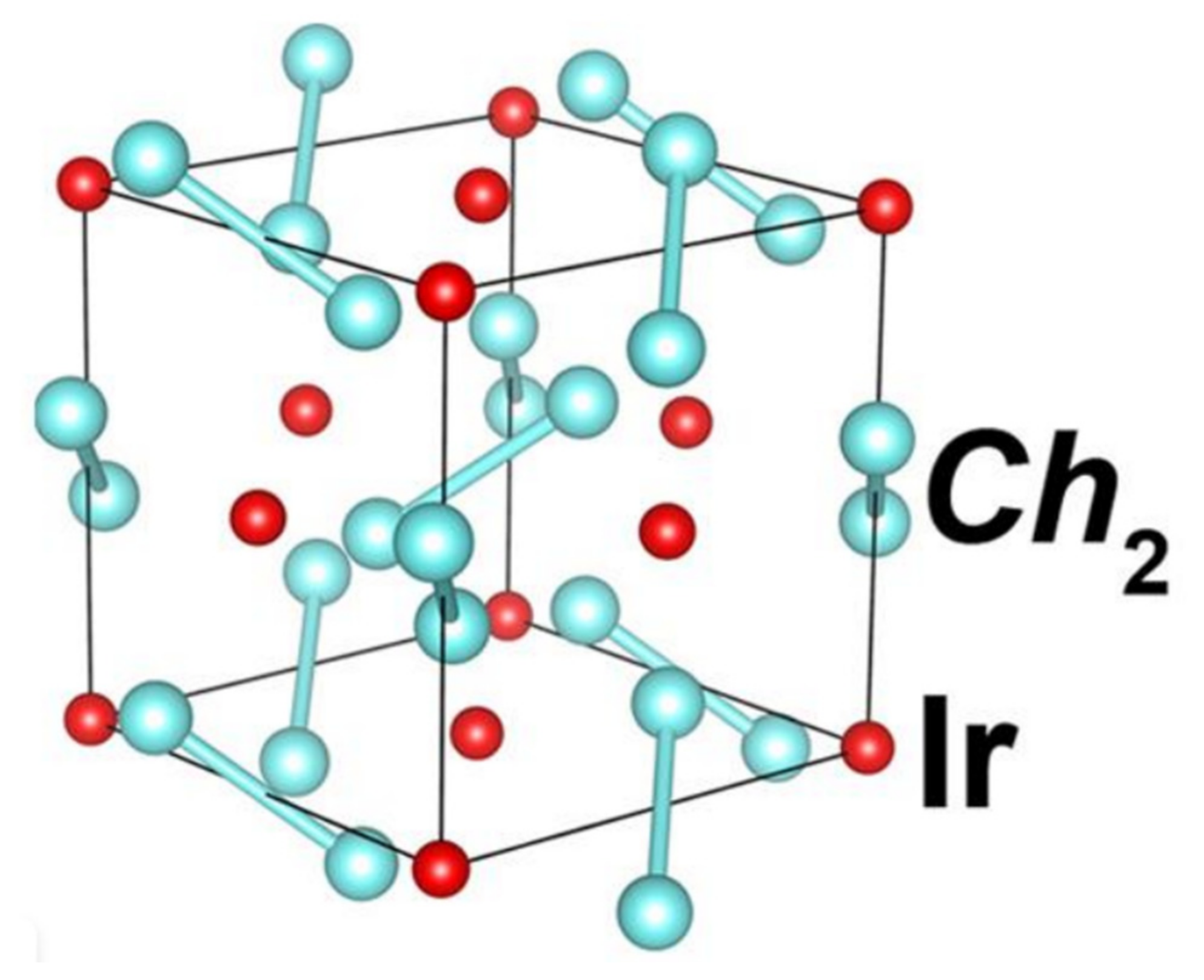
  103. Qi, Y.; Matsuishi, S.; Guo, J.; Mizoguchi, H.; Hosono, H. Superconductivity in Defective Pyrite-Type Iridium ChalcogenidesIrxCh2(Ch = Seand Te). Phys. Rev. Lett. 2012, 109, 217002.
  104. Gor’Kov, L.P.; Rashba, E.I. Superconducting 2D System with Lifted Spin Degeneracy: Mixed Singlet-Triplet State. Phys. Rev. Lett. 2001, 87, 037004.
  105. Frigeri, P.A.; Agterberg, D.F.; Sigrist, M. Spin susceptibility in superconductors without inversion symmetry. New J. Phys. 2004, 6, 115.
  106. Frigeri, P.A.; Agterberg, D.F.; Koga, A.; Sigrist, M. Superconductivity without Inversion Symmetry: MnSi versusCePt3Si. Phys. Rev. Lett. 2004, 92, 097001.
  107. Bauer, E.D.; Hilscher, G.; Michor, H.; Paul, C.; Scheidt, E.W.; Gribanov, A.V.; Seropegin, Y.; Noël, H.; Sigrist, M.; Rogl, P. Heavy Fermion Superconductivity and Magnetic Order in NoncentrosymmetricCePt3Si. Phys. Rev. Lett. 2004, 92, 027003.
  108. Settai, R.; Sugitani, I.; Okuda, Y.; Thamizhavel, A.; Nakashima, M.; Ōnuki, Y.; Harima, H. Pressure-induced superconductivity in CeCoGe3 without inversion symmetry. J. Magn. Magn. Mater. 2007, 310, 844–846.
  109. Kimura, N.; Ito, K.; Aoki, H.; Uji, S.; Terashima, T. Extremely High Upper Critical Magnetic Field of the Noncentrosymmetric Heavy Fermion SuperconductorCeRhSi3. Phys. Rev. Lett. 2007, 98, 197001.
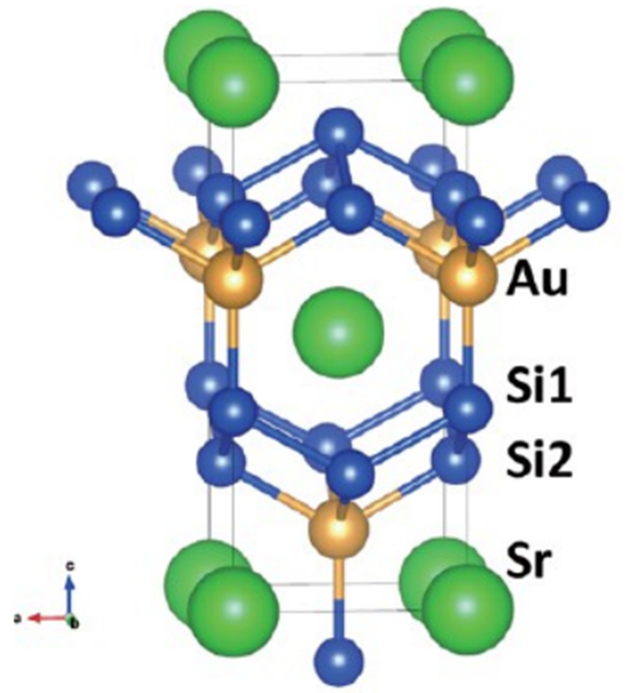
  110. Isobe, M.; Yoshida, H.; Kimoto, K.; Arai, M.; Takayama-Muromachi, E. SrAuSi3: A Noncentrosymmetric Superconductor. Cheminform 2014, 26, 2155–2165.
  111. Pyon, S.; Kudo, K.; Matsumura, J.-I.; Ishii, H.; Matsuo, G.; Nohara, M.; Hojo, H.; Oka, K.; Azuma, M.; Garlea, V.O.; et al. Superconductivity in Noncentrosymmetric Iridium Silicide Li2IrSi3. J. Phys. Soc. Jpn. 2014, 83, 1–5.
  112. McMillan, W.L. Transition Temperature of Strong-Coupled Superconductors. Phys. Rev. 1968, 167, 331–344.
  113. Dynes, R. McMillan’s equation and the Tc of superconductors. Solid State Commun. 1972, 10, 615–618.
  114. Zheng, X.; Zheng, J. Seeking high temperature superconductors in ambient from exemplary beryllium-based alloys. Solid State Commun. 2019, 306, 113769.
  115. Ryu, G.; Kim, S.W.; Mizoguchi, H.; Matsuishi, S.; Hosono, H. Superconductivity in a PbFCl-type pnictide: NbSiAs. Eur. Lett. 2012, 99, 27002.
  116. Mizoguchi, H.; Hosono, H. La2Sb, a layered superconductor with metal–metal bonds. Chem. Commun. 2011, 47, 3778–3780.
  117. Guo, J.; Yamaura, J.-I.; Lei, H.; Matsuishi, S.; Qi, Y.; Hosono, H. Superconductivity in Ban+2Ir4nGe12n+4(n = 1,2) with cage structure and softening of low-lying localized mode. Phys. Rev. B 2013, 88, 1–5.
  118. Ryu, G.; Kim, S.W.; Matsuishi, S.; Kawaji, H.; Hosono, H. Superconductivity in Nb4MSi (M = Ni, Co, and Fe) with a quasi-two-dimensional Nb network. Phys. Rev. B 2011, 84, 1–6.
  119. Li, Y.; Weng, Y.; Zhang, J.; Ding, J.; Zhu, Y.; Wang, Q.; Yang, Y.; Cheng, Y.; Zhang, Q.; Li, P.; et al. Observation of superconductivity in structure-selected Ti2O3 thin films. NPG Asia Mater. 2018, 10, 522–532.
  120. Jeong, S.; Matsuishi, S.; Lee, K.; Toda, Y.; Kim, S.W.; Hosono, H. Superconductivity of Ca2InN with a layered structure embedding an anionic indium chain array. Arxiv Prepr. 2014, arXiv:1403.1348.
  121. Arpaia, R.; Golubev, D.; Baghdadi, R.; Ciancio, R.; Dražić, G.; Orgiani, P.; Montemurro, D.; Bauch, T.; Lombardi, F. Transport properties of ultrathin YBa2Cu3O7−δ nanowires: A route to single-photon detection. Phys. Rev. B 2017, 96, 064525.
  122. Stepantsov, E.A.; Arpaia, R.; Lombardi, F. Growth of twin-free b-oriented YBa2Cu3O7 − x films. Crystallogr. Rep. 2015, 60, 393–396.
  123. Stepantsov, E.A.; Lombardi, F.; Winkler, D. Growth of YBa2Cu3O7 films with tilt of CuO planes to the surface on SrTiO3 crystals. Crystallogr. Rep. 2011, 56, 152–156.
  124. Kislinskii, J.; Zhao, B.-R.; Wu, P.-J.; Peng, Z.-Q.; Chen, Y.-F.; Yang, T.; Chen, L.; Sun, J.-J.; Xu, B.; Wu, F.; et al. YBa2Cu3O7 Bicrystal Josephson Junctions and dc SQUIDs. Chin. Phys. Lett. 1996, 13, 390–393.
  125. Carillo, F.; De Luca, G.M.; Montemurro, D.; Papari, G.P.; Salluzzo, M.; Stornaiuolo, D.; Tafuri, F.; Beltram, F. Coherent transport in extremely underdoped Nd1.2Ba1.8Cu3Oznanostructures. New J. Phys. 2012, 14, 1–10.
  126. Chaix, L.; Ghiringhelli, G.; Peng, Y.; Hashimoto, M.; Moritz, B.; Kummer, K.; Brookes, N.; He, Y.; Chen, S.; Ishida, S.; et al. Dispersive charge density wave excitations in Bi2Sr2CaCu2O8+δ. Nat. Phys. 2017, 13, 952–956.
More