Your browser does not fully support modern features. Please upgrade for a smoother experience.
Please note this is a comparison between Version 1 by Sayyar Shah and Version 2 by Sirius Huang.
Molybdenum disulfide (MoS2), with a two-dimensional (2D) structure, has attracted huge research interest due to its unique electrical, optical, and physicochemical properties. MoS2 has been used as a co-catalyst for the synthesis of novel heterojunction composites with enhanced photocatalytic hydrogen production under solar light irradiation. Nanostructured MoS2 can be fabricated via both top-down and bottom-up approaches.
- photocatalysis
- heterojunction
- layers structure materials
- hydrogen production
1. Introduction
Molybdenum disulfide (MoS2), with a 2D nanostructure, has attracted huge attention due to its outstanding optical and electronic properties and promising applications [1][2][3][4][5]. MoS2 nanomaterials as co-catalysts are promising photocatalysts for hydrogen evolution reaction (HER) [1][6]. It is reported that the exposed edges of layers of MoS2 contain active sites for catalytic activity while its basal planes are mostly inactive [2][7].
Nanostructured MoS2 can be fabricated via both top-down and bottom-up approaches. In the case of the top-down method, the commercially available bulk crystal of MoS2 is physically downsized into MoS2 nanomaterials (Figure 1) [8][9][10][29,40,41], while in the bottom-up approach, MoS2 nanomaterials are synthesized via chemical reaction with small molecules using chemical vapor deposition (CVD) and hydrothermal or solvothermal methods, etc. [11][12][13][42,43,44]. Single layers, multilayers, nanoparticles, and quantum dots of MoS2 have also been reported [14][15][16][17][45,46,47,48]. Continued efforts have been reported for the fabrication of MoS2 nanomaterials via the top-down and bottom-up strategies [8][9][10][11][12][13][18][19][20][21][22][23][24][16,17,18,19,28,29,30,31,40,41,42,43,44].
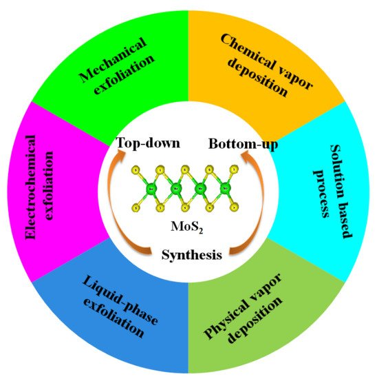
Figure 1. Various synthetic methods for MoS2 preparation.
2. Top-Down Approach
Exfoliation of MoS2
Due to the layered structure and van der Waals interactions, MoS2 nanosheets can be easily prepared through the exfoliation method. Mechanical, chemical, electrochemical, and liquid-phase exfoliation processes have been reported for the synthesis of MoS2 nanosheets [1][2][3][4][5][9][10][11][12][13][14][15][16][17][39,40,41,42,43,44,45,46,47,48,49,50,51,52]. For example, in the mechanical exfoliation technique, the suitable MoS2 flakes are peeled off from the bulk crystal of MoS2 using adhesive tape and shifted onto a specific substrate [6][15][46,53]. When the scotch tape is detached, some parts of MoS2 remain on the substrate. As result, single- or few-layer MoS2 nanosheets with random shapes and sizes are obtained. The 2D materials prepared by the exfoliation method have good quality and allow to study the pristine properties of materials and device performance. However, during this process, the thickness and size of the MoS2 are difficult to control, and the resulting materials are inappropriate for large-scale production and scaled-up applications [6][7][53,54]. Li et al., mechanically exfoliated single- and multilayer MoS2 nanosheets from SiO2/Si with the adhesive tape method [10][41]. The flakes of MoS2 were mechanically stripped on Si/SiO2 substrate. The obtained single-layer and multilayer MoS2 materials were characterized using a bright-field optical microscope and an atomic force microscope (AFM). From the AFM measurements, the height of a single MoS2 sheet was found to be 0.8 nm, while the thickness of two, three, and four layers of MoS2 nanosheets was 1.5, 2.1, and 2.9 nm, respectively (Figure 2). The MoS2 nanosheet monolayers showed an enhanced optical performance, especially single-layer MoS2 nanosheets. It was observed that the van der Waals interactions between MoS2 to SiO2 were much weaker. For this purpose, gold can be used as a substrate to exfoliate the MoS2 nanosheets due to its strong affinity for sulfur. It can exfoliate the MoS2 monolayer from the bulk because of the strong van der Waals interactions between Au and MoS2 layers [25][26][27][55,56,57]. Huang et al. prepared large-area MoS2 nanosheets using a Au-assisted exfoliation strategy [3][50]. In a typical synthesis, a Au thin layer was deposited on a Ti or Cr adhesion-covered substrate. To develop good contact between a MoS2 bulk crystal on tape and a Au-covered substrate, it should be passed under high pressure. The monolayer sheets with a large area were collected from the surface of the Au after peeling off the tape.
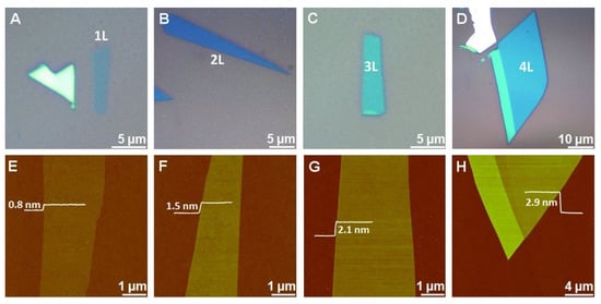
Figure 2. Mechanically exfoliated single- and multilayer MoS2 nanosheets on Si/SiO2. (A–D) Optical microscope and (E–H) AFM images of MoS2 nanosheets. The single MoS2 sheet thickness is 0.8 nm (E), while the thickness of two (F), three (G), and four (H) layers of MoS2 nanosheets is 1.5, 2.1, and 2.9 nm, respectively. Reprinted with permission from Ref. [41]. Copyright 2012 Wiley-VCH Verlag GmbH & Co.
In the top-down approaches, single- and multilayer MoS2 nanosheets are prepared, which have been used to study some fundamental properties of MoS2 nanosheets.
3. Bottom-Up Approach
3.1. Chemical Vapor Deposition
The CVD technique has a long history and is commonly used for the synthesis of high-quality semiconductor materials. In a typical CVD process of MoS2 nanosheets, the Mo sources are solid precursors of Mo or MoO3 powder, and the S sources are H2S gas or solid S powder [28][29][30][31][58,59,60,61]. The solid MoO3 and vaporized S react with each other in a low-pressure chamber, forming nuclei for the growth of MoS2 [28][58]. Then, MoS2 slowly grows and enlarges its size on the substrates under carrier gas flow. The temperatures at which MoS2 grows during the CVD process are usually between 700 and 1000 °C, with a metal catalyst such as Au [31][61]. Plasma-enhanced CVD requires a low temperature (150–300 °C) for the growth of MoS2 nanosheets, and MoS2 can even be directly deposited on the plastic substrate [32][62]. Recently, metal organic CVD has been reported for the synthesis of MoS2 nanosheets [33][34][63,64], where organometallic precursors were used as starting materials.
3.2. Physical Vapor Deposition
Advanced technology such as molecular beam epitaxy (MBE) can be used to prepare single-crystal semiconductor thin films. However, its applications are limited to the synthesis of 2D materials [35][65]. Ordinary physical vapor deposition is rarely reported for 2D materials. A MoS2–Ti composite was prepared by direct current magnetron sputtering, using Ti and MoS2 materials [36][66]. In this process, the MoS2 was amorphous.
3.3. Solution-Based Process
Solution-based processes are commonly used to synthesize MoS2 nanosheets. Hydrothermal and solvothermal methods are the most interesting for the preparation of MoS2 nanosheets [37][38][67,68]. In these methods, the Mo source is commonly a molybdate, such as Na2MoO4 or (NH4)6Mo7O24, and the S source is thiourea and thioacetamide and L-cysteine [39][40][41][42][43][69,70,71,72,73]. The molybdate reacts with the S or S compound in a stainless steel autoclave. The physicochemical reaction takes place at high temperatures (160–200 °C) and pressure for at least a few hours. In the solvothermal method, organic solvents such as 1-methyl-2-pyrrolidinone, N,N-dimethylformamide, and polyethylene glycol-600 are used to proceed with the reaction, while in the hydrothermal method, water is used as a solvent. The MoS2 powders obtained from these methods have different sizes and shapes. The sizes and shapes of the products can be adjusted by altering the experimental conditions. To improve the crystalline quality of MoS2, the products are usually post-annealed at high temperature.
The MoS2 nanomaterials prepared through different bottom-up approaches have various sizes, shapes, morphologies, and thicknesses and can be used for many applications.