Your browser does not fully support modern features. Please upgrade for a smoother experience.
Please note this is a comparison between Version 1 by DANIAL KHAN and Version 2 by Vivi Li.
With the advancement of beyond-CMOS devices to keep Moore’s law alive, several emerging devices have found application in a wide range of applications. Spintronic devices offer low power, non-volatility, inherent spatial and temporal randomness, simplicity of integration with a silicon substrate, etc. This makes them a potential candidate for next-generation hardware options. This work e xplores the giant spin Hall effect (GSHE)-driven spin-orbit torque (SOT) magnetic tunnel junction (MTJ) as a potential candidate for creating an externally triggered hardware Trojan and insertion into logic-locked hardware security considering the effect of process and temperature variations is explored.
- giant spin Hall effect (GSHE)
- hardware security
- hardware trojan
- magnetic tunnel junction (MTJ)
- spintronics
- spin-orbit torque (SOT)
- spin-transfer torque (STT)
1. Introduction
In recent years, the increasing trend of outsourcing integrated circuits (ICs) design and fabrication in their foundries has led the semiconductor companies to rely on third party fabrication facilities [1]. This approach helped to cut costs and accelerated time-to-market, but it also raised serious concerns about whether an IP owner and a third party can establish trust [2]. A number of attacks such as IC overproduction [3], IC cloning [4], IP piracy [5], and hardware Trojan insertion [6] can be carried out by an untrusted foundry. For off-shore fabrication to stay secure, the capability of the IP owner must be thoroughly proven to prevent such attacks. Hardware Trojan insertion is a malicious modification in the original IC design during the fabrication process by the attackers [7][8][7,8]. It can lower the IC security by leaking confidential information, causing field malfunctioning, or even destroying the IC using predesigned conditions [9]. Therefore, a hardware Trojan can cause profit loss in consumer devices and be life-threatening if used in military devices. Hence, rwesearchers can say that the hardware Trojan is a significant threat to both the government and other organizations that require security for their systems.
Figure 1a shows the taxonomy of the hardware Trojan, and the highlighted flow represents the targeted levels for designing the Trojan in this work. Figure 1b represents the taxonomy for Trojan detection based on pre-silicon and post-silicon stages. Figure 1c shows the block diagram of the system-on-chip (SoC) design flow with the targeted Trojan insertion at a later stage in the SoC design flow, thus bypassing primarily pre-silicon tests. Test time detection techniques compare side-channel behavior [9][10][9,10] and/or functional verification of the suspected ICs to the “golden model” (Trojan-free IC model). The suspected IC is classified as Trojan infected if it differs significantly from the golden model. However, whether golden models can be generated for real-world applications still remains an open question.
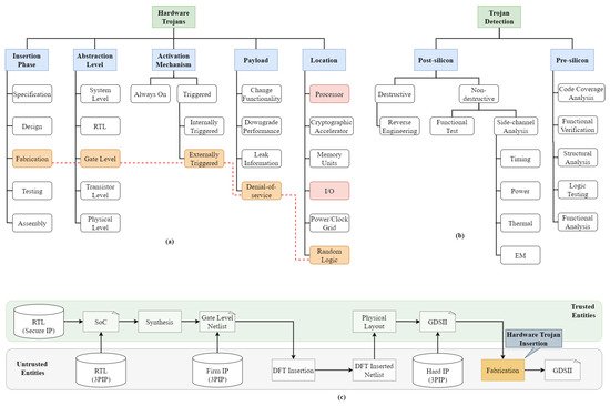
Figure 1.
(
a
) Taxonomy of hardware Trojans and selected flow for this work. (
b
) Taxonomy of hardware Trojan detection. (
c
) System-on-chip (SoC) design flow.
2. Background
2.1. Hardware Trojan (HT)
Malicious modification at the hardware level can cause altered IC functionality, leading to disastrous results in security applications. Conventional design-time verification and post-fabrication techniques may not be sufficient to counter emerging hardware Trojan made from emerging beyond-CMOS devices such as spintronic devices, memristors, carbon nanotubes (CNTs), and nanowire FETs (NWFETs), etc. References [11][12][13][14][15][16][17][18][19][13,14,15,16,17,18,19,20,21] evaluated the performance and reliability of CNT bundles for on-chip interconnect applications due to their large conductivity and current carrying capabilities. Reference [20][22] presents a comprehensive model for the resistance in graphene nanoribbon (GNR) interconnects. One of ouresearchers' future goals is to explore spintronics devices for memory and/or logic applications, and even for interconnects due to their low-power consumption, non-volatility, and high endurance compared to CMOS technology. CMOS-based hardware Trojans consist of (1) a trigger part that determines when Trojans get activated and (2) a payload that decides what type of changes will happen once the Trojans are triggered. The trigger part usually contains digital or analog counter circuits activated only when certain conditions are satisfied. Spintronic-based Trojans have various advantages over CMOS Trojans. Spintronic hardware Trojans depend on external factors like magnetic field and temperature due to their unique physical characteristics, which can be exploited for external triggering. The hybrid CMOS and MTJ circuits [21][23] can replace some of the logic gates, and careful designing can make them implement the same functionality with competitive switching, area, and energy consumption compared to the CMOS gates. Reference [22][24] reports that the amplitude of low-order leakages in masked implementations can be amplified externally by tweaking side-channel measurement setups in a way that is under the control of a power analysis adversary.2.2. Magnetic Tunnel Junction (MTJ)
Figure 2a shows a typical MTJ structure comprising two relatively thick ferromagnetic layers (fixed layer and free layer) separated by a relatively thin tunnel barrier layer. When the fixed and free layers have the same magnetic direction (parallel, denoted by P), the MTJ shows a lower resistance (RP). On the contrary, when the magnetic directions of both layers are opposite (anti-parallel, denoted by AP), the MTJ shows a higher resistance (RAP). The tunnel magnetoresistance (TMR) ratio characterizes the resistance difference and is defined by the following equation:
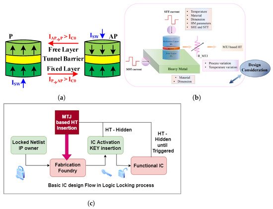
Figure 2. (a) A p-MTJ structure and switching between the two states. (b) Design consideration for SOT-MTJ. (c) Basic IC design flow in the logic-locking process.
Here, m and mr are the unit vector along with magnetization of the free layer and the reference layer, respectively, γ is the gyromagnetic ratio, μ0 is the vacuum permeability, Heff is the effective magnetic field, α is the Gilbert damping coefficient, P is the polarization factor, JSTT and JSHE are the spin-transfer torque (STT) and spin-orbit torque (SOT) current density applied to the MTJ device, and σSHE is the polarization direction of the spin current injected in the free layer. Figure 2b shows the design consideration for the SOT-MTJ for creating the hardware Trojan.
MTJ has found several applications in hardware security applications like logic locking [23][26], physically unclonable functions (PUFs) [24][27], true random number generators (TRNGs) [25][28], etc. In this work, rwesearchers designed a hardware Trojan based on SOT-assisted STT-MTJ with an externally initiated triggering (external magnetic field) mechanism. This mechanism allows the Trojan to remain hidden until an external magnetic field of the desired magnitude is applied in the appropriate direction. Due to the unique response of the Trojan block to certain external factors, it may remain hidden to a great extent from the verification process [26][29]. RWesearchers have explored Trojan insertion in the logic-locking-based security in this work. The robustness to all detection and verification processes during IC design is currently beyond the work’s scope. However, primary Trojan detection methods, as shown in Figure 1b. Nevertheless, new emerging beyond-CMOS devices hold many security concerns and solutions [27][30]. When both the foundry and user are not trusted, logic locking is widely used to ensure hardware security. The hidden Trojans can bypass the logic-locking mechanism if they operate in the functional IC. The limitations are malfunctioning only for the duration of the external condition, vulnerability to new verification methods to counter it, inability to attack inactivated ICs, design complexity, etc.
3. Hardware Trojan Operation
3.1. Circuit Description of Hardware Trojan (HT) Block
In the proposed work, a compact model of SOT-assisted PMA MTJ-based on the Verilog-A behavioral model [28][31] is used. The LLG solver described in the Verilog-A model is used to solve the magnetic dynamics of the MTJ. A detailed switching mechanism for the model is provided in [21][23]. The MTJ-based hardware Trojan block is shown in Figure 3b. It consists of a pre-charge sense amplifier (PCSA), SOT-assisted MTJ, writing circuit, MOS logic circuitry, and a multiplexer, as shown in Figure 3a. PCSA provides the output in TRUE as well as in complementary form. It is used to sense the outputs of the circuit based on the MTJ state, whether it is parallel or anti-parallel. The resistance of MTJ is low in the parallel state compared to the resistance in the anti-parallel state. In one branch of PCSA, rwesearchers have a SOT-MTJ and the logic circuitry of MOSFETs, whereas, in another branch, researcherswe have a reference resistance to compare the resistances of both branches. Depending on the MOS logic circuitry, the switching of MTJ state occurs, and hence the resistance varies. The read path used to read the state of MTJ is also shown in Figure 3a. A multiplexer is used at the output of PCSA to select the desired operation.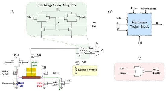
Figure 3. (a) Detailed circuit operation of hardware Trojan block. (b) Block diagram of Trojan with input and output lines. (c) Generation of write enable signal for Trojan block.
The writing circuit for the MTJ comprises four NMOS transistors (MN3–MN6). A reset signal is applied to reset the MTJ to the default state. The reset signal allows the current to flow from supply voltage to the ground through the heavy metal of MTJ and transistors MN5 and MN4. During the writing phase, the write enables signal is made HIGH so that the current flows from the heavy metal through the transistors MN3 and MN6. The amount of current is based on the logic circuitry of PMOS transistors (MP1–MP2). The reset, write, and read paths are shown in Figure 3a using blue, red, and green arrows, respectively.
To write the MTJ correctly, the write enables signal must be turned ON under the following conditions. The first condition is that the clock pulse should be LOW, and the other condition is that the reset signal should be OFF at that time. The condition is displayed using a NOR gate in Figure 3c. If reset, Clk, and write enable signal are made HIGH at the same time, then all three paths (reset, write, and read path) will turn ON simultaneously, and the circuit will perform the false operation. The ability of this kind of architecture to produce complementary output can be utilized to initiate multiple threats. Several counters or timer-based circuits can be designed to activate polymorphic logic. Careful designing of triggering mechanisms and verification will be essential in such cases.
3.2. Logic Locking
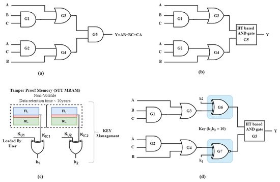
Logic locking [29][32] is a technique that inserts new key inputs and logic mechanisms into the circuit, causing the circuit to behave incorrectly until the correct key combination is provided to the circuit. Various logic-locking techniques have been proposed to protect the privacy and integrity of ICs. When the foundry and user are not trusted, logic locking is the best way to ensure hardware security. The hardware Trojan, which has a low probability of activating, thus can be made operational only when the IC is activated. The logic-locking block will not allow the IC to work. External factors required to trigger the Trojan and the IC can be made to malfunction only after activation. In Figure 4a, a logic circuit designed using logic gates displaying output Y = AB + BC + CA is present. All gates (G1–G5) are designed using 40 nm CMOS technology. To insert the Trojan block in the circuit, the gate G5 performing AND operation is replaced by a Trojan-based block performing the same operation, as shown in Figure 4b. In logic locking-based hardware security, key management is essential as the attacker aims to obtain the key. Figure 4c shows how the keys are stored in a tamper-proof memory to keep them safe from attackers. These memory units are fabricated on the chip so that the keys are not known to the foundry [30][33]. Some logically locked blocks are inserted between the logic circuit in Figure 4b so that the correct output is present when the true key is applied. The modified logic circuit is presented in Figure 4d, where the XOR and XNOR gates are used as logically locked blocks. The key for the circuit shown in Figure 4d is k1k2 = 10. For all other values of k1k2, the circuit will provide incorrect output.
Figure 4. (a) Unlocked netlist with Y = AB + BC + CA. (b) G5 replaced with MTJ-based hardware Trojan block. (c) Key management for logic locking block. (d) Locked netlist with MTJ-based hardware Trojan block.
