Your browser does not fully support modern features. Please upgrade for a smoother experience.
Please note this is a comparison between Version 1 by Jian Fu Zhang and Version 2 by Camila Xu.
CMOS technology dominates the semiconductor industry, and the reliability of MOSFETs is a key issue. Negative bias temperature instability (NBTI) and positive bias temperature instability (PBTI) mainly degrade the performance of pMOSFETs and nMOSFETs, respectively.
- reliability
- instability
- aging
- degradation
- bias temperature instability (BTI)
1. Introduction
Failures of electronic products have been commonly encountered in our daily life, and there is no way that a product can be made with a zero failure rate. Different products require different levels of reliability. For example, the failure rate in auto-electronic components must be lower than that in electronic toys. Failure can be broadly divided into two types: permanent breakdown and temporary malfunction, where a product can recover by, for example, restarting it. Failure rate can be improved by sacrificing performance such as speed and power consumption. A successful commercial product should have a well-balanced trade-off between the failure rate, performance, and costs.
Ever since CMOS was invented in 1963, its reliability has always been a key issue [1][2][3][4][5][6][7][8][9][10][11][12][13][14][15][16][17][18][19][20][21][22][23][24][25][26][27][28][29][30][31][32][33][34][35][36][37][38][39][1,2,3,4,5,6,7,8,9,10,11,12,13,14,15,16,17,18,19,20,21,22,23,24,25,26,27,28,29,30,31,32,33,34,35,36,37,38,39]. Failure occurs at both the frontend [1][2][3][4][1,2,3,4], where MOSFETs are located, and the backend [5][6][5,6]. The backend includes multiple metal layers for connections and low-k dielectrics between these layers. The metal wires suffer from electromigration [5], where metal atoms gradually migrate from their initial locations, eventually resulting in open or short circuits. To minimize time delay, the dielectric between these metal wires must have low dielectric constants, making them vulnerable to both mechanical and electrical breakdown [6].
There are different types of instability for MOSFETs at the frontend including mobile ions [7], hot carriers [8][9][8,9], time-dependent dielectric breakdown (TDDB) [10], bias temperature instabilities (BTIs) [1][2][3][4][1,2,3,4], and random telegraph noise (RTN) [11][12][13][11,12,13]. Their relative importance changes with time. To show this change, rwesearchers named one type as the dominant instability for each decade after the invention of CMOS in Figure 1. In the 1960s and 1970s, mobile ions in gate oxide, such as sodium ions (Na+), were a major concern [7]. They originate from contamination and have been effectively eliminated by using cleanroom technologies.
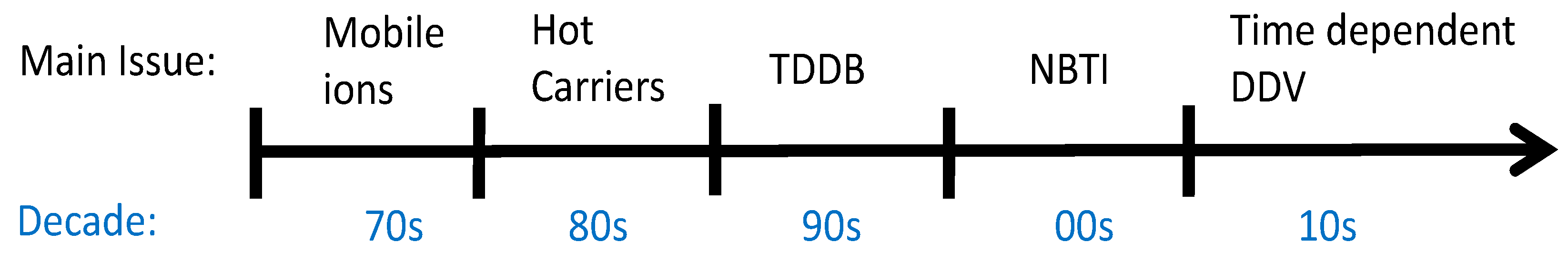
Figure 1. The main reliability issue in each decade for CMOS technologies. DDV: device-to-device variation.
The main reliability issue in each decade for CMOS technologies. DDV: device-to-device variation.
In 1980s, the operation voltage was kept at 5 V when device sizes were downscaled as shown in Figure 2. This leads to an increase in the electrical field, which accelerates charge carriers in the conduction channel and makes them “hot”. Through impact and ionization, hot carriers can cause damage to devices by generating interface states and forming space charges in gate oxides, which reduce the driving current, Id, under a given bias [8][9][8,9]. A typical definition for device lifetime is the time for an Id reduction of 10% [8][9][8,9], and hot-carrier-induced aging limited device lifetime in the 1980s.

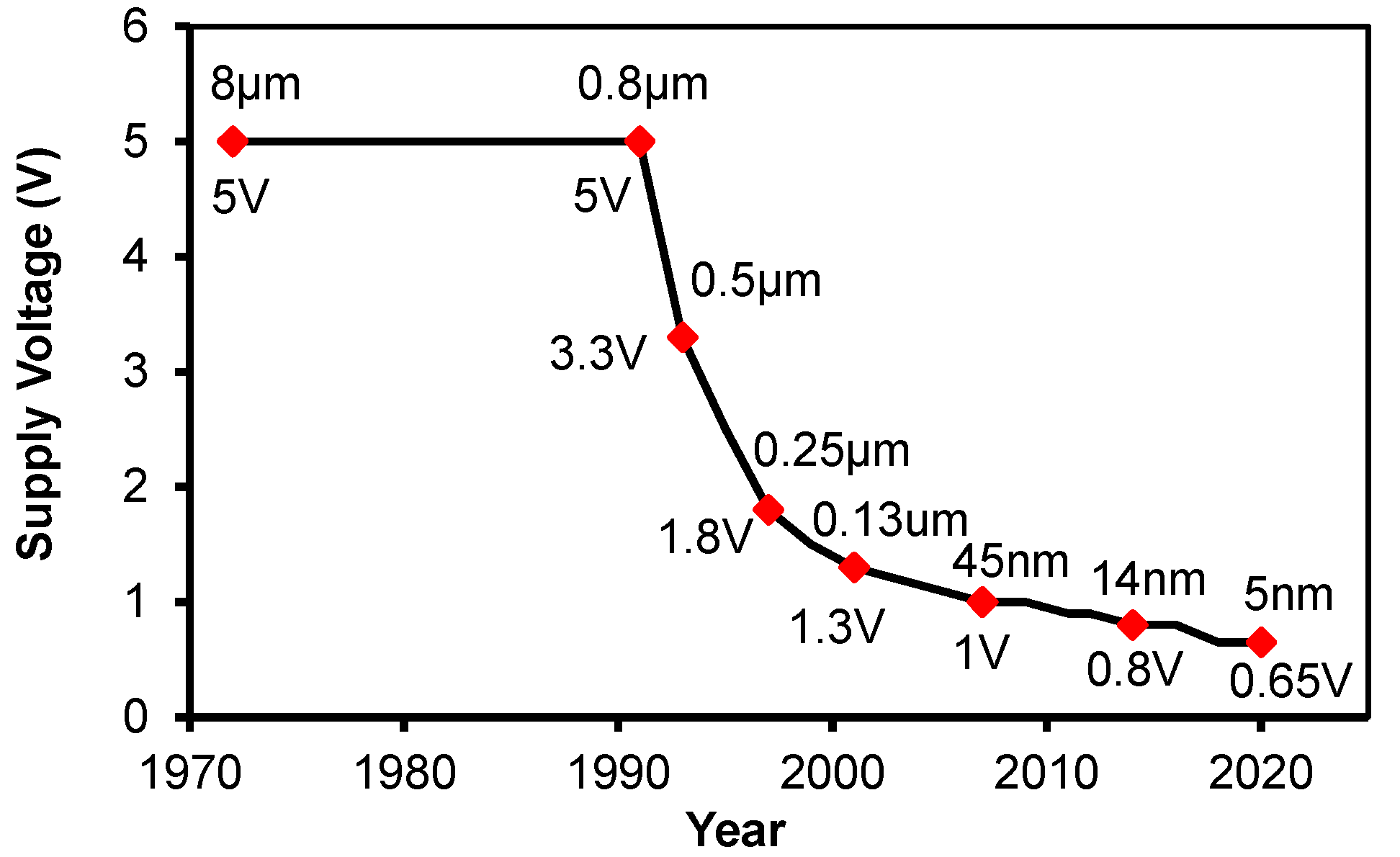
Figure 2. The supply voltage of different generations of CMOS technologies. It was fixed at 5 V before 1990s but has been reduced with the downscaling of device sizes since 1990.
In 1990s, the continuous reduction in the operation voltage, as shown in Figure 2, reduced the relative importance of hot carrier aging. Gate oxides became sufficiently thin, and direct tunneling occurred through them. This causes damage to gate oxides. The damage accumulates and eventually triggers oxide breakdown. As the damage accumulation takes some time, the breakdown is referred to as time-dependent dielectric breakdown (TDDB). TDDB was the dominant reliability issue in the 1990s [10].
In 2000s, negative bias temperature instability (NBTI) of pMOSFETs became the lifetime-limiting instability and attracted much attention [14][15][16][17][18][19][20][21][22][14,15,16,17,18,19,20,21,22]. The difference between hot carrier aging (HCA) and NBTI is that HCA occurs mainly near the drain junction, while NBTI happens uniformly. Before high-k dielectrics were used, silicon dioxides were nitrided to form oxynitrides, which increases NBTI [14]. BTI was also a major barrier to overcome in developing high-k processes [23][24][25][23,24,25].
Since 2010s, devices have become so small that device-to-device variations (DDVs) are a major challenge to circuit design. In addition to the static as-fabricated DDVs [26], device aging is stochastic and introduces time-dependent variation (TDV) [27][28][29][30][31][27,28,29,30,31]. Both HCA and BTI contribute to TDV. Moreover, for nanoscale devices, a single trap in the gate dielectric can capture a carrier from the conduction channel and induce considerable change of Id in the form of random telegraph noise (RTN) [11][12][13][11,12,13]. RTN is different from aging: aging shifts device parameters in one direction, while RTN causes their fluctuation in both directions. This further complicates the characterization and modeling of TDV.
 Before 2000, the gate oxide used to study NBTI was relatively thick (e.g., >4 nm) and the oxide field applied was generally too low for electrons to tunnel through the oxide [1][2][3][1,2,3]. These NBTI works are hereafter referred to as “pre-2000 NBTI”. Under these conditions, NBTI has the following features:

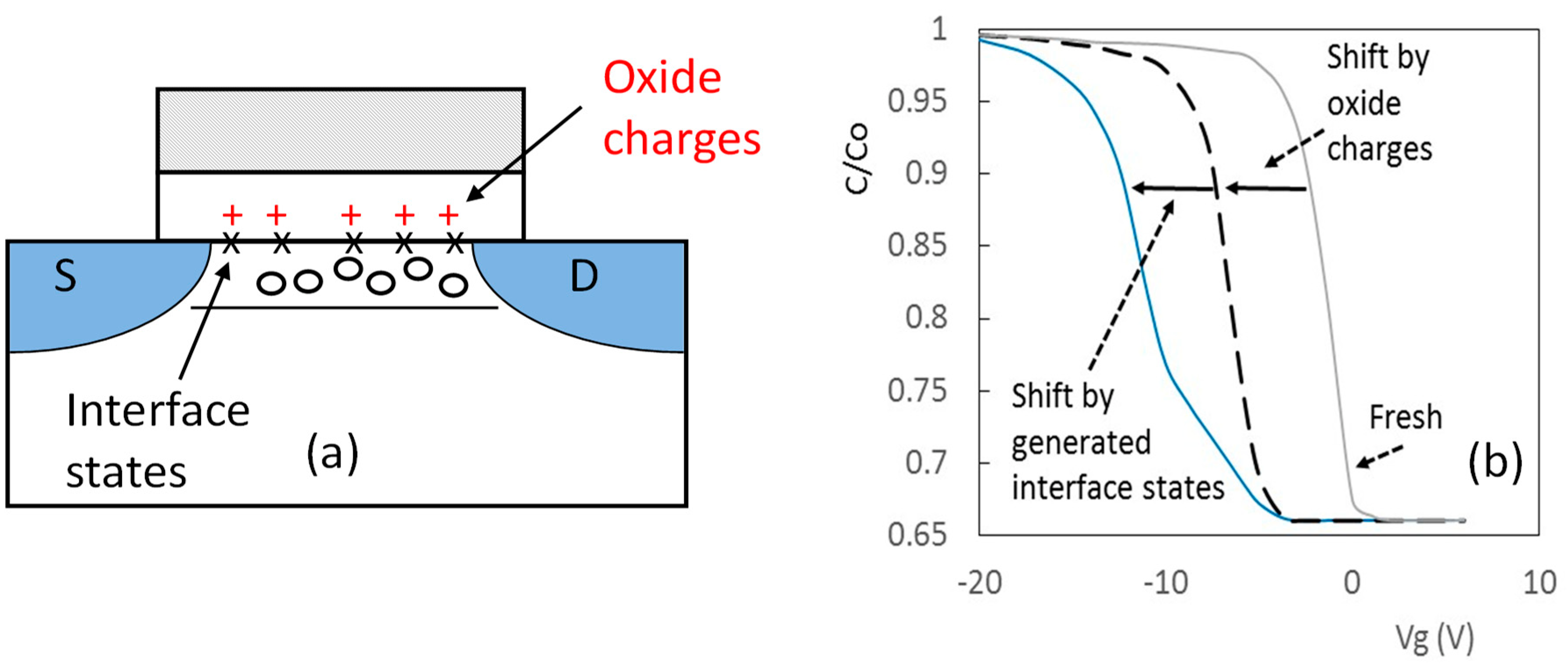
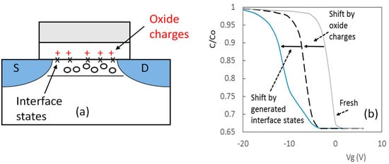
 On the physical process, the Si–H bond at the interface is generally believed to be the precursor for generated interface states [17]. During NBTI stress, Si–H is ruptured, and the released hydrogenous species then migrate into the gate oxide, leaving behind the Si dangling bond, also commonly known as the Pb-center, as the interface state [2][4][17][2,4,17]. The generated interface states in the lower half of Si bandgap are donor-like. As gate bias is swept in the negative direction, there are an increasing amount of them moving above the Fermi-level at the interface, Ef, and becoming positively charged. This leads to the nonparallel shift in CV as shown in Figure 3b.
In addition to the nonparallel shift, there is also a parallel negative shift, as shown in Figure 3b, which is caused by positive charges formed in the oxide. The magnitude of parallel shift is similar to that of nonparallel shift in Figure 3b, indicating a one-to-one correlation between the oxide charges and the positive charges from the generated interface states. This, however, does not mean that the oxide charge density is equal to the density of the generated interface states. As each Pb-center has two states, one acceptor-like in the upper-half of Si bandgap and one donor-like in the lower half of bandgap, the interface state density measured using a popular technique, such as charge pumping, should double the oxide charge density.
On the aging kinetics, it was proposed that the power law results from the diffusion of hydrogenous species through gate oxides as the rate limiting process [2][4][2,4]. This hypothesis was challenged as the gate oxide of modern MOSFETs is too thin and the time for hydrogenous species diffusing through it is too short to limit the aging process [17].
On the physical process, the Si–H bond at the interface is generally believed to be the precursor for generated interface states [17]. During NBTI stress, Si–H is ruptured, and the released hydrogenous species then migrate into the gate oxide, leaving behind the Si dangling bond, also commonly known as the Pb-center, as the interface state [2][4][17][2,4,17]. The generated interface states in the lower half of Si bandgap are donor-like. As gate bias is swept in the negative direction, there are an increasing amount of them moving above the Fermi-level at the interface, Ef, and becoming positively charged. This leads to the nonparallel shift in CV as shown in Figure 3b.
In addition to the nonparallel shift, there is also a parallel negative shift, as shown in Figure 3b, which is caused by positive charges formed in the oxide. The magnitude of parallel shift is similar to that of nonparallel shift in Figure 3b, indicating a one-to-one correlation between the oxide charges and the positive charges from the generated interface states. This, however, does not mean that the oxide charge density is equal to the density of the generated interface states. As each Pb-center has two states, one acceptor-like in the upper-half of Si bandgap and one donor-like in the lower half of bandgap, the interface state density measured using a popular technique, such as charge pumping, should double the oxide charge density.
On the aging kinetics, it was proposed that the power law results from the diffusion of hydrogenous species through gate oxides as the rate limiting process [2][4][2,4]. This hypothesis was challenged as the gate oxide of modern MOSFETs is too thin and the time for hydrogenous species diffusing through it is too short to limit the aging process [17].

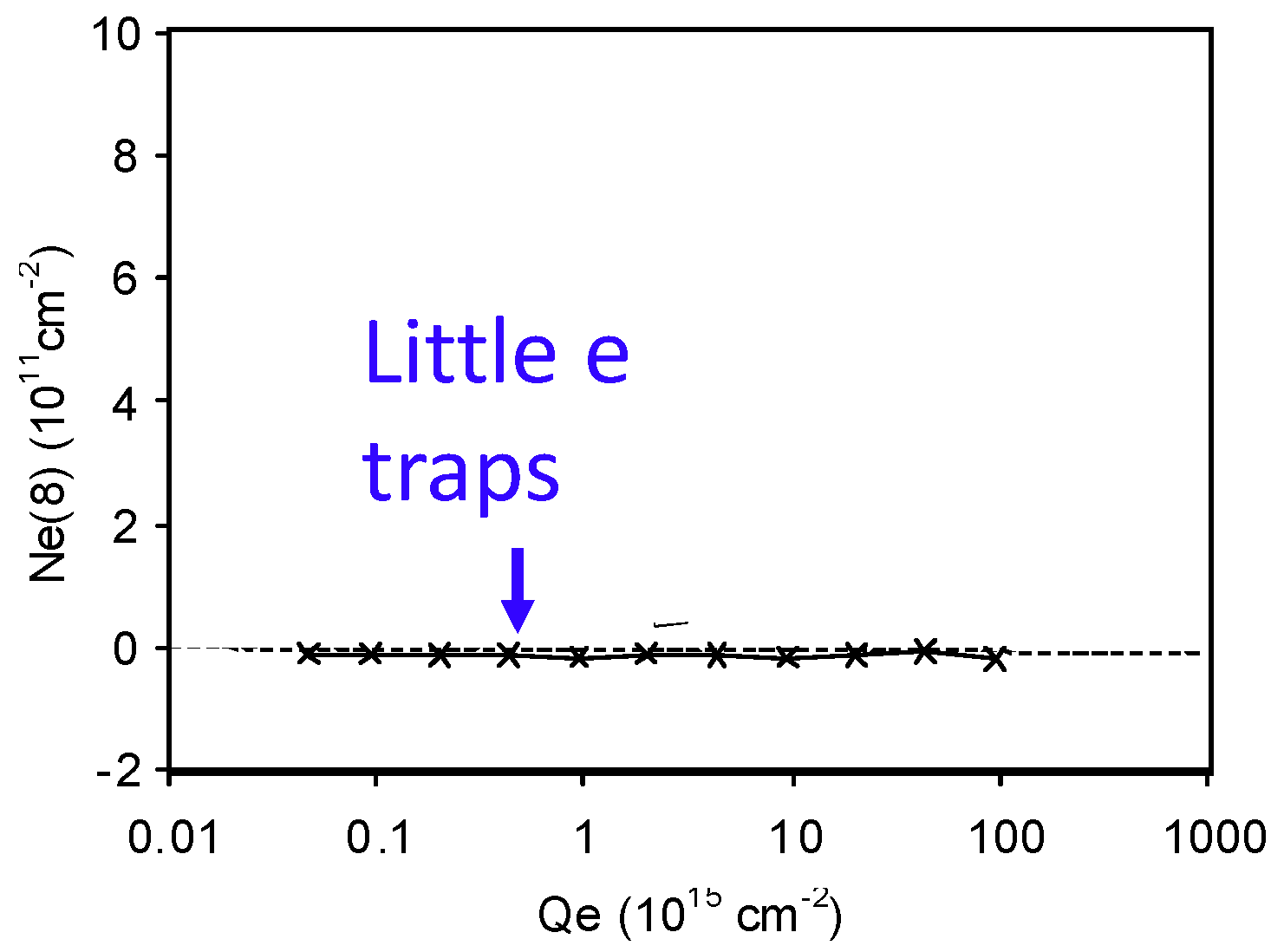
 When poly-si was used as the gate for the self-aligned CMOS processes, the high temperature anneal after gate implantation effectively drives these hydrogenous species out of SiO2. Figure 736 shows that there were little as-grown electron traps for poly-si gated SiO2, and electron traps must be generated by carrier tunneling through the oxide under a high oxide field [46][62]. When gate SiO2 is relatively thick (e.g., >5 nm), electron tunneling through gate oxide during operation is negligible, so that PBTI is insignificant. For thinner SiO2, tunneling carriers can create new electron traps. These electron traps can act as stepping-stones to form the gate-induced leakage current. They do not form stable space charges in the gate oxide and PBTI is again insignificant.
When the high-k/SiON stack is used, PBTI becomes considerable. In the early stage of high-k process development, PBTI was so severe that it limited the commercial use of the process as detailed in the next section.
When poly-si was used as the gate for the self-aligned CMOS processes, the high temperature anneal after gate implantation effectively drives these hydrogenous species out of SiO2. Figure 736 shows that there were little as-grown electron traps for poly-si gated SiO2, and electron traps must be generated by carrier tunneling through the oxide under a high oxide field [46][62]. When gate SiO2 is relatively thick (e.g., >5 nm), electron tunneling through gate oxide during operation is negligible, so that PBTI is insignificant. For thinner SiO2, tunneling carriers can create new electron traps. These electron traps can act as stepping-stones to form the gate-induced leakage current. They do not form stable space charges in the gate oxide and PBTI is again insignificant.
When the high-k/SiON stack is used, PBTI becomes considerable. In the early stage of high-k process development, PBTI was so severe that it limited the commercial use of the process as detailed in the next section.
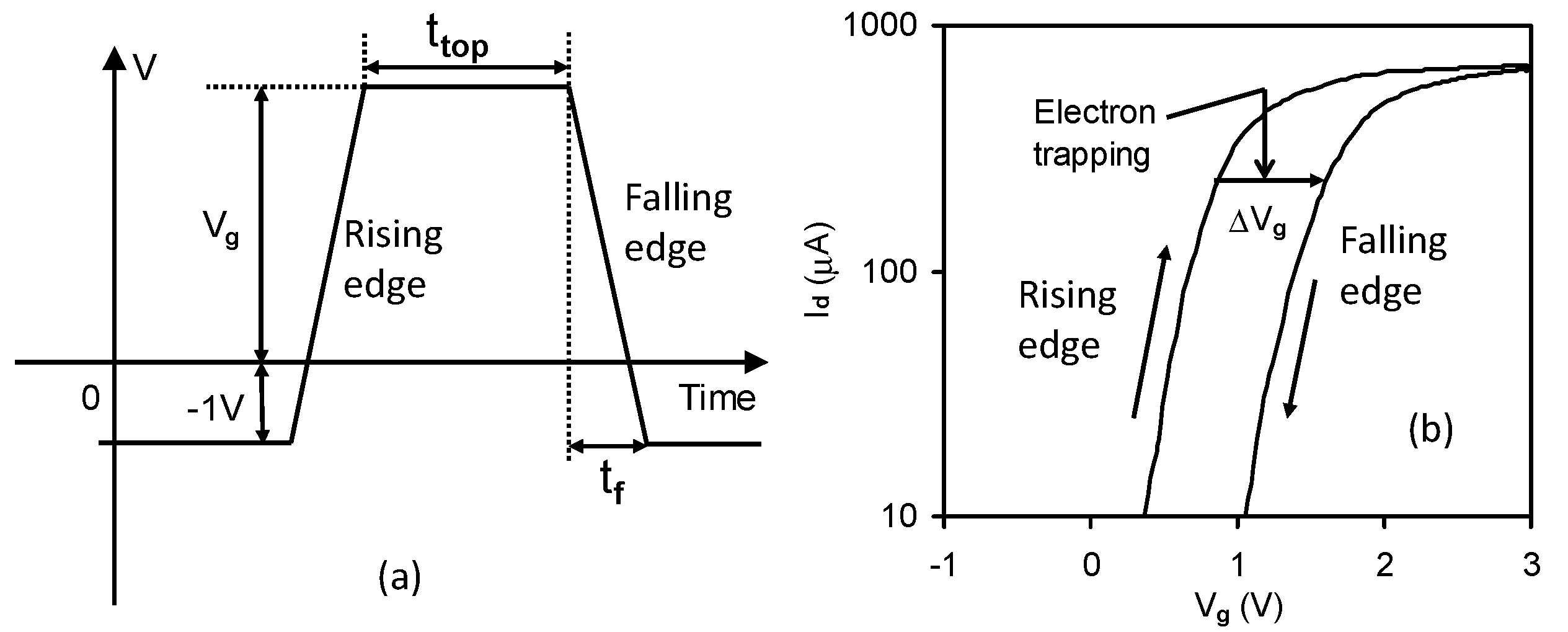
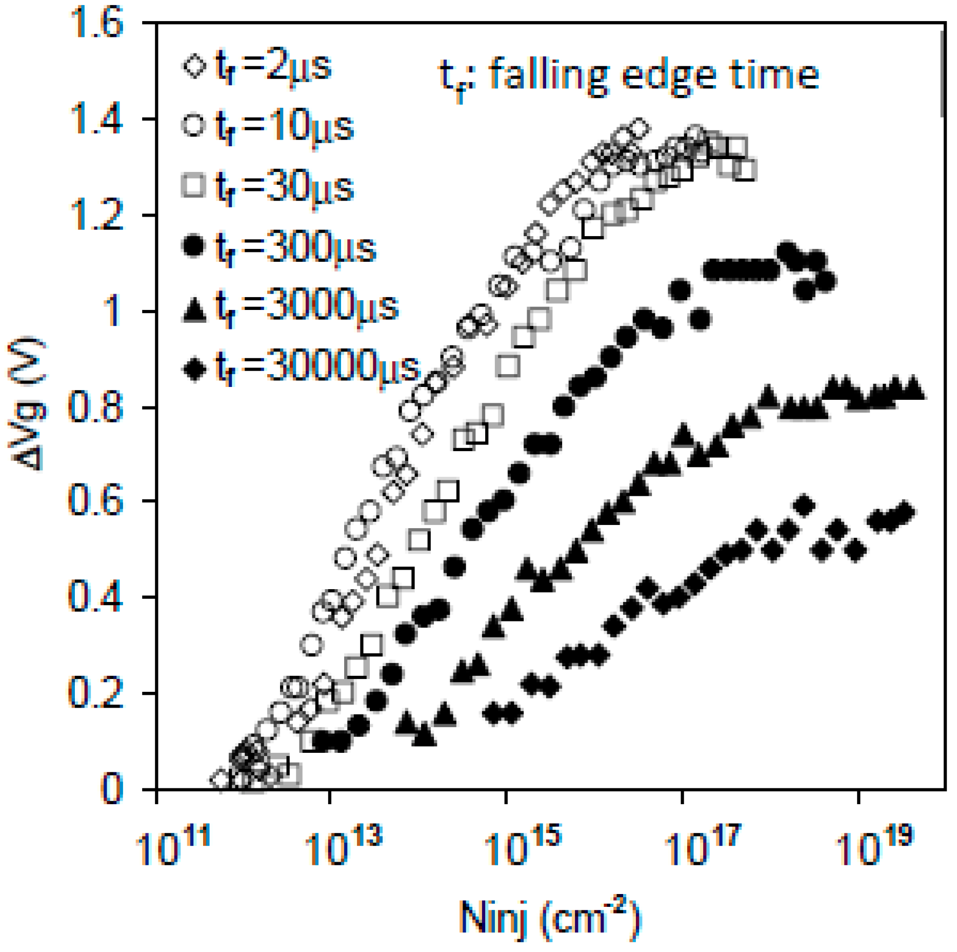
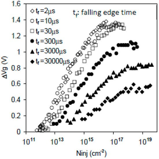
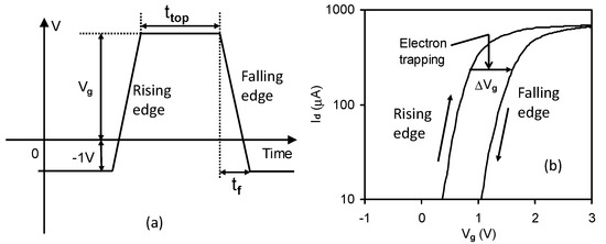 Figure 938 shows that trapped electrons are not stable, and some of them can be lost when the falling edge time is longer than 30 μs [47][63]. As a result, the energy level of these electron traps is shallow and above the lower edge of silicon conduction band, Ec. These traps are as-grown and can be repeatedly charged and discharged [47][63].
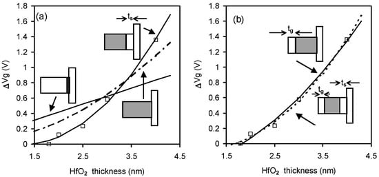
 Significant efforts have been made to overcome this huge PBTI. To find the location of these as-grown electron traps, the PBTIs of different HfO2 thicknesses were measured in Figure 1039. The grey regions are the assumed trap locations. It can be seen that neither a pile-up of traps at the high-k/SiO2 interface nor a uniform distribution of traps in the high-k layer agree with the test data. Good agreement was obtained by assuming there were no traps around 1.3~1.8 nm at one or both ends of the high-k layer [47][63]. Figure 11 40 shows that PBTI reduced rapidly as the high-k layer became thinner.

 The absence of electron trapping near the end of the high-k layer could be because electrons there can escape to the electrodes and will not form a steady space charge. It is also possible that thick high-k layer could be partially crystallized, resulting in the shallow traps. The suppression of these shallow traps by using thin high-k layers has allowed their commercial use since the advent of 45 nm CMOS technology in 2007.
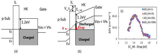
 To characterize the electron traps responsible for PBTI, their energy profile was probed. After charging them, as shown in Figure 1342a, they were gradually lifted above the Si Ec to allow them to discharge as shown in Figure 1342b [48][55]. The discharging at different energy levels resulted in the energy profiles in Figure 1342c. These electron traps were below Si Ec under flat band conditions and peaked around 1.4 eV below the conduction band edge of HfO2.
 Like NBTI, the as-grown defects for PBTI can be divided into as-grown electron traps (AETs) and energy alternating defects (EADs). The energy levels of the AETs did not change with charging–discharging, while the energy levels of the EADs were lowered following charging as shown in Figure 1544. This difference allows for their separation as shown in Figure 1544 [39].
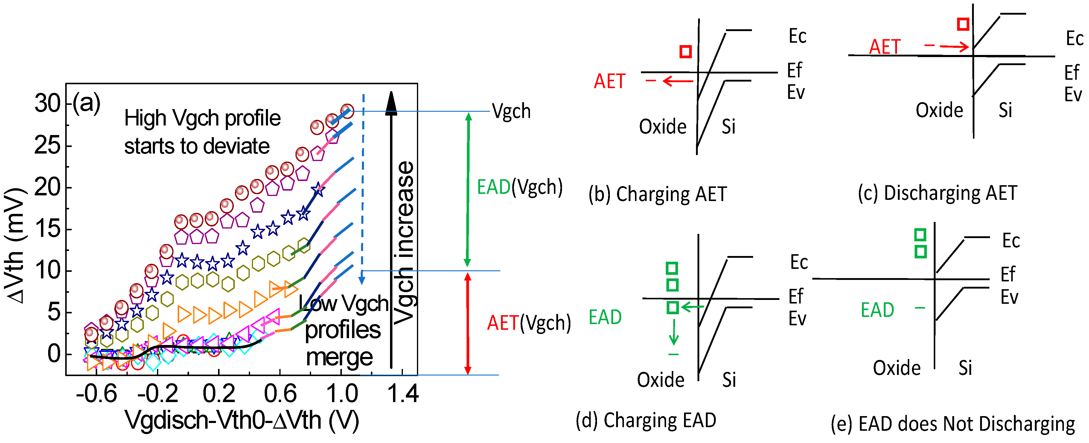
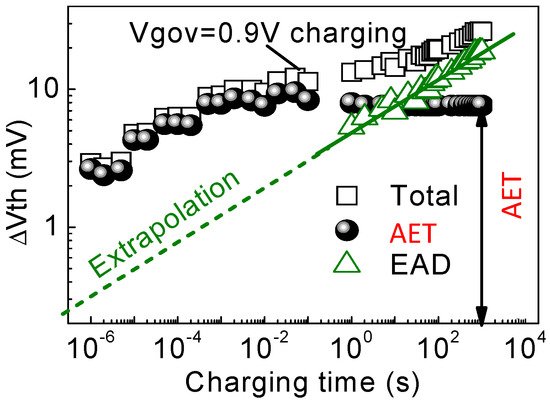
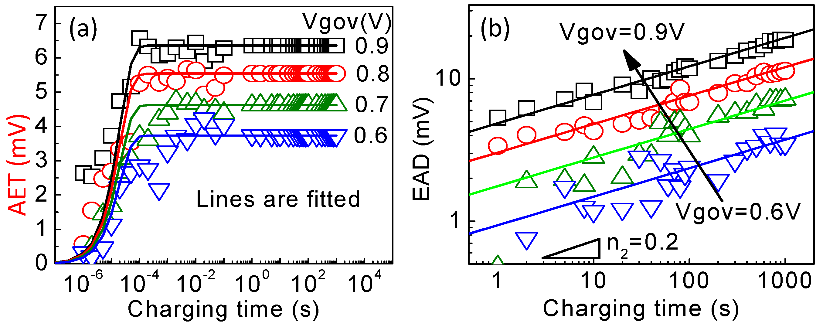
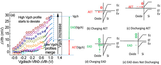 On filling kinetics, an AET can be filled rapidly, and it saturates with time. On the other hand, filling an EAD follows a power law. The saturation level of AET is determined from the measurement in Figure 1544a. This saturation level is then subtracted to obtain the EAD after the AET saturation as shown by the green triangles in Figure 1645. These EAD data were fitted with a power law. To obtain the AET before its saturation, the EAD power law was extrapolated to short time as shown by the green, dashed line. An AET over a short time was evaluated by subtracting the extrapolated EAD as shown by the circles in Figure 1645.
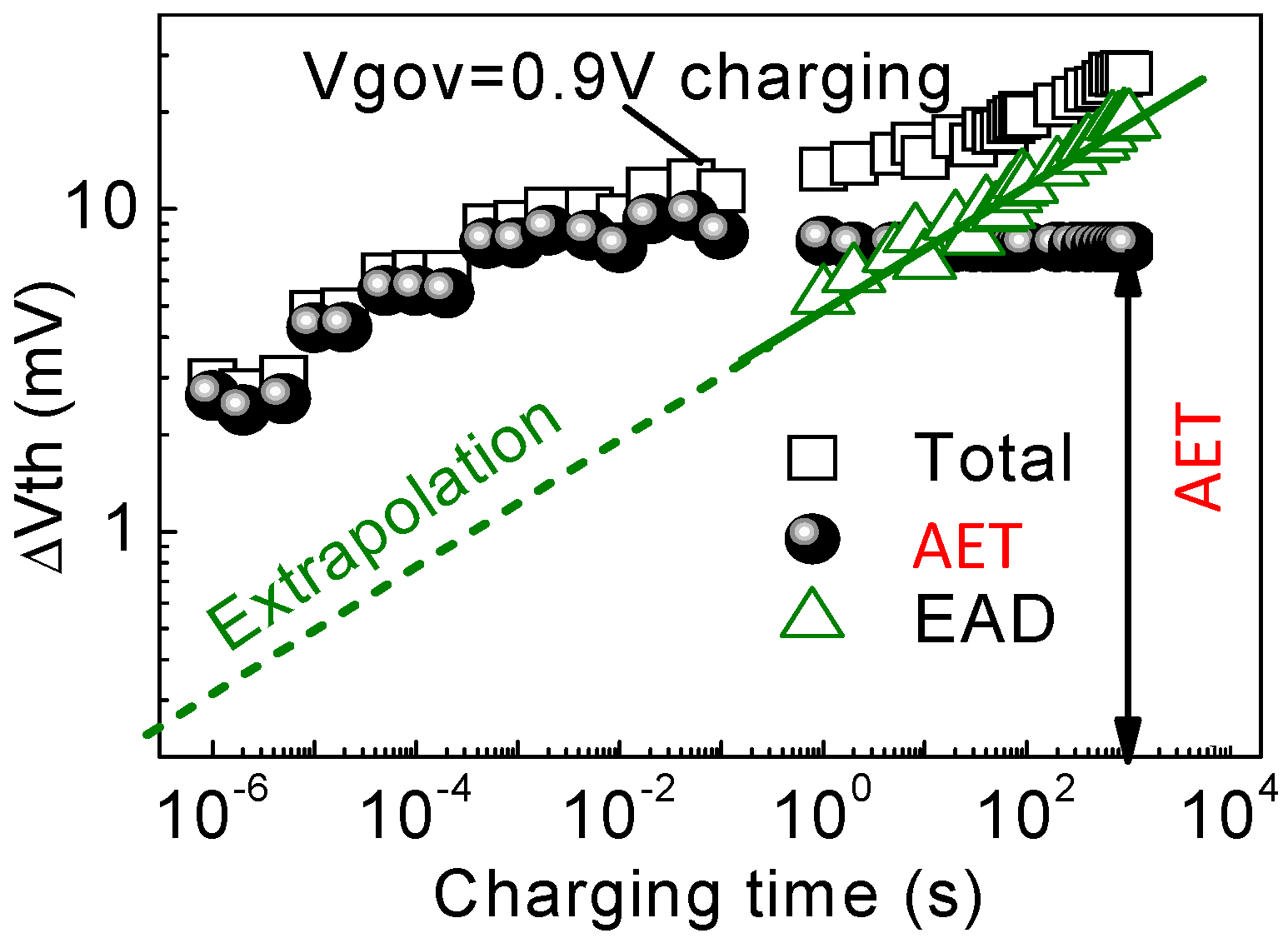
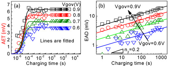
 The separated AET and EAD at different Vgov are given in Figure 1746a,b, respectively. The power exponent of the EAD was insensitive to Vgov, and the AET followed the same kinetics after normalizing against their saturation level.
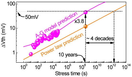 The stress–discharge–recharge (SDR) technique in Figure 26 can also be applied to PBTI. After removing the contribution of as-grown defects, Figure 2049a shows that the power exponent extracted from the generated defects measured by the SDR technique became independent of the measurement conditions. Moreover, Figure 2049b shows that the power exponent was insensitive to the stress bias.
 By combining the modeling of as-grown defects with that of generated defects, the as-grown-generation model in Table 1 can also be applied to PBTI [39]. Figure 1948 shows that the AG model can be used to predict the PBTI at low bias.
2. Negative Bias Temperature Instability (NBTI)
NBTI and PBTI mainly degrade the performance of pMOSFETs and nMOSFETs, respectively. Early attention was focused on NBTI, as it is generally higher than PBTI and limits the lifetime of pMOSFETs. We review NBTI first, followed by PBTI in Section 3.2.1. Pre-2000 NBTI
NBTI was reported only a few years after the invention of CMOS technology and is one of the earliest instabilities observed for MOSFETs [1]. Under a negative gate bias, positive charges build up both in the gate oxide and from the generated interface states as shown in Figure 3a. This results in a negative shift in the capacitance–voltage (CV) characteristics, as shown in Figure 3b [1], and an increase in the magnitude of the threshold voltage of pMOSFETs [17].Figure 3. (a) A schematic illustration of oxide charges and the generated interface states; (b) the effect of NBTI on capacitance versus gate voltage characteristics: positive charges in gate oxide lead to a parallel shift and the generated interface states result in a nonparallel shift [1][17][1,17].
-
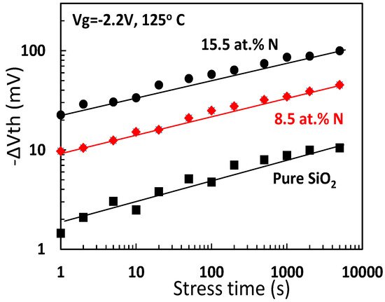
Figure 4 shows that NBTI follows power law against stress time. The power exponent is insensitive to gate bias and temperature [14];
-
Its recovery is insignificant;
-
It also follows power law against gate bias;
-
It is thermally activated.
3. Positive Bias Temperature Instability (PBTI)
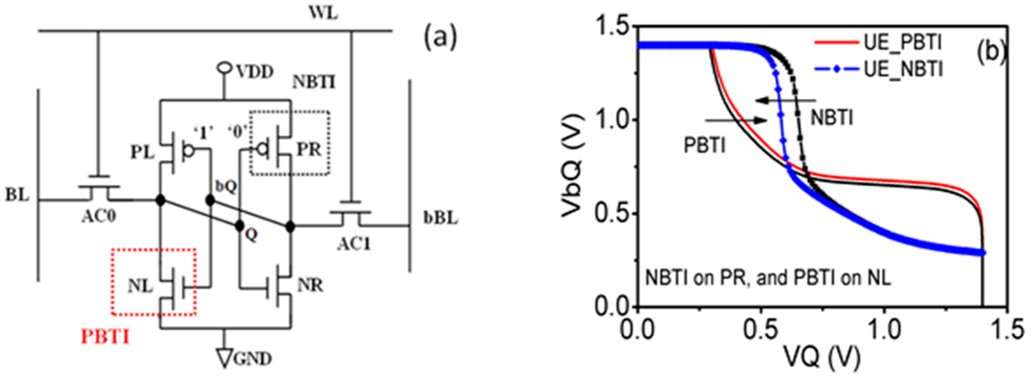
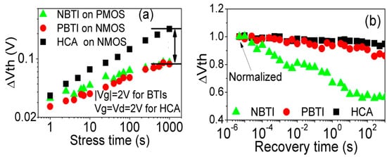
As pMOSFETs and nMOSFETs are switched on by negative and positive gate bias, respectively, NBTI mainly affects pMOSFETs, while PBTI mainly affects nMOSFETs. The relative importance of PBTI against NBTI is process dependent [23][24][25][23,24,25], and their impact on circuits can be added together rather than cancelling each other out. For example, Figure 534a shows that for a SRAM cell, NBTI and PBTI stresses occur in different inverters, making one inverter different from the other. Both NBTI and PBTI contribute to the reduction of the static noise margin, which is proportional to the size of butterfly eyes in Figure 534b [29]. As a result, both require modeling to optimize circuit performance.Figure 534. (a) When a SRAM cell holds a data bit, PBTI occurs in one of the pull-down nMOSFETs, while NBTI happens in the pull-up pMOSFET of the opposite inverters; (b) both PBTI and NBTI contribute to the reduction in the static noise margin (i.e., the size of butterfly eyes) by making the two inverters imbalance [29].
3.1. History of PBTI
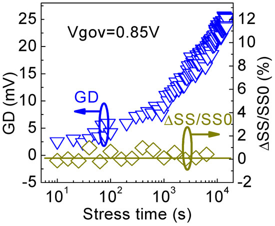
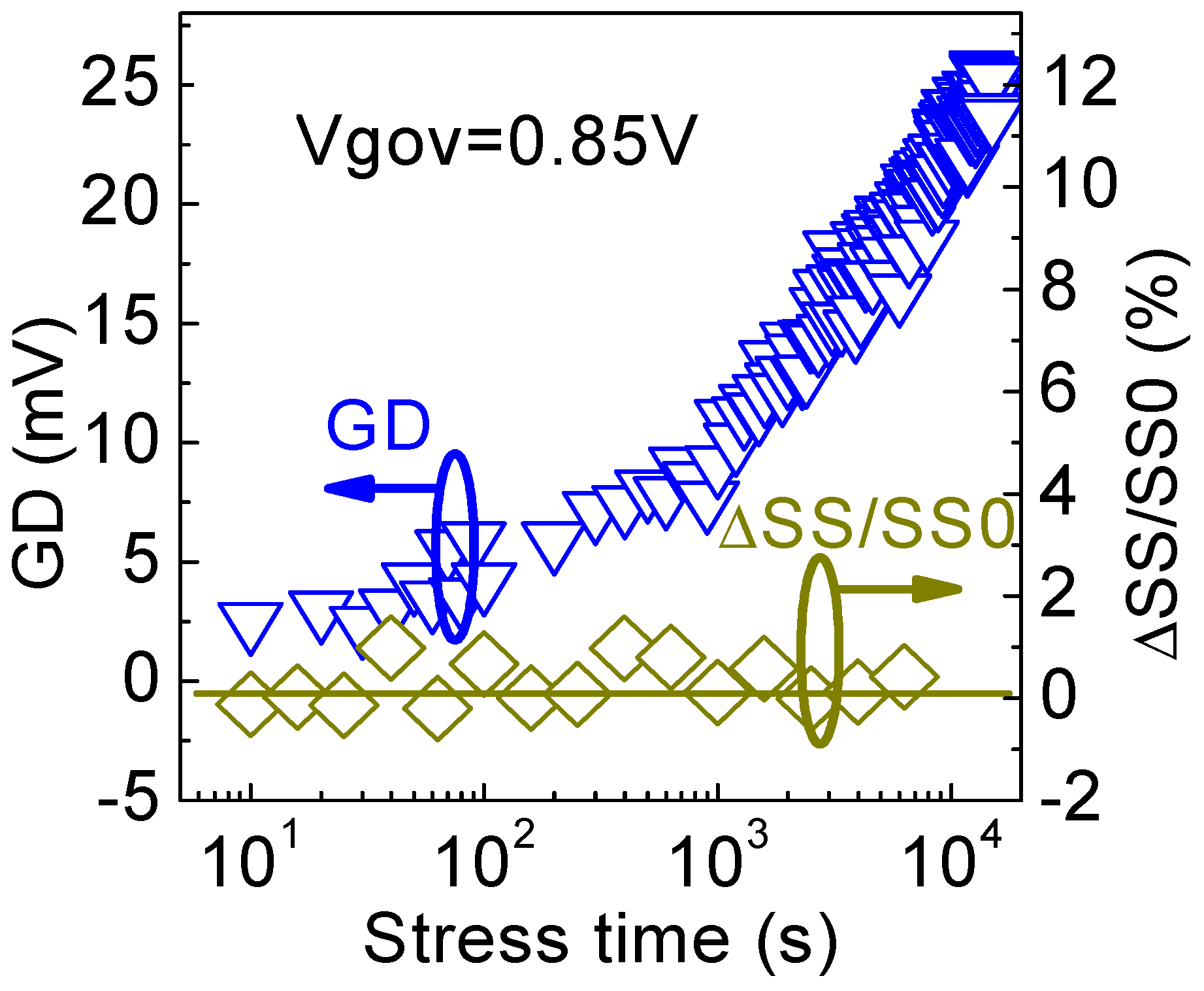
Figure 631 shows that NBTI originates from both generated interface states and positive charges formed in the interfacial region of gate oxide. In contrast, Figure 35 shows that interface states are not created for PBTI, so that PBTI only originated from negative charge formation in the gate dielectric through filling acceptor-like electron traps [40][41][42][43][44][45][56,57,58,59,60,61]. Early works showed that, if arsenium, a common dopant for Si, was left in the gate oxides, they formed electron traps [40][56]. Water diffused into SiO2 produces electron traps with a well-defined capture cross section of 10−17 cm2 [41][57]. When aluminum was used as the gate in early generation CMOS technologies, hydrogenous species also induced smaller traps with capture cross-section on the order of 10−18 cm2 [42][43][44][45][58,59,60,61].Figure 635. Under positive gate bias, generated defects (GDs) increased, but the negligible change in subthreshold swing (SS) indicates that interface states were not created [39].
3.2. PBTI as the Limiting Instability during the Early Stage of High-k Process Development
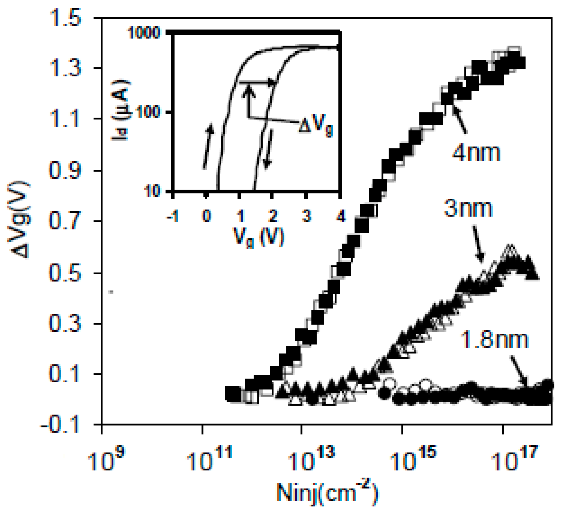
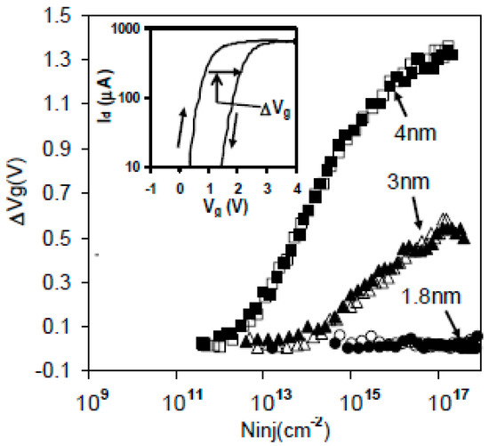
Figure 837a,b show the PBTI of a HfO2 (4 nm)/SiO2 (1 nm) stack during the development of the high-k process [24][25][24,25]. The Id-Vg recorded for the rising and falling Vg pulse edges in Figure 837a is compared in Figure 837b. The Id-Vg recorded at the falling edge was shifted in the positive direction by over half a volt from the Id-Vg of the rising edge. This was caused by electron trapping under a positive Vg during the top period of several microseconds.Figure 837.
(
a
) The gate bias waveform; (
Figure 938. An increase in the falling edge time resulted in a lower trapping level because the trapped electrons can be detrapped before the measurement [47].
An increase in the falling edge time resulted in a lower trapping level because the trapped electrons can be detrapped before the measurement [63].
Figure 1039.
The location of as-grown electron traps in HfO
2. Symbols represent the test data, and the lines are fitted with traps located in the grey regions [47].
. Symbols represent the test data, and the lines are fitted with traps located in the grey regions [63].
Figure 1140.
The rapid reduction of as-grown electron trapping with the downscaling of the thickness of HfO
3.3. PBTI of Modern High-k/SiON Stacks
Although the suppression of shallow as-grown electron traps has reduced PBTI significantly, PBTI still exists in modern commercial CMOS processes with high-k/SiON stacks [9][39][48][9,39,55]. One example is given in Figure 412a, which shows that PBTI is comparable with NBTI [9]. Moreover, Figure 412b shows that the recovery of PBTI is substantially less than that of NBTI. It confirms that these electron traps are energetically deeper than those responsible for the PBTI in the early stage of high-k process development as shown in Figure 837. When compared with hole traps for NBTI that pile up at the dielectric/substrate interface, the electron traps for PBTI were relatively distant from the dielectric/Si interface [47][49][43,63], which also contribute to the relative stability of PBTI.Figure 412. A comparison of PBTI with NBTI during stress (a) and recovery (b). (a) Shows that the PBTI was similar to NBTI during stress for this CMOS process but more stable during recovery [9].
Figure 1342. Probing the energy distribution profile of electron traps: (a) the electron traps below Si Ec were first charged; (b) applying a positive Vg will lift some charged traps above Ec for discharging, i.e., the striped region; (c) the extracted energy profile of electron traps by progressively increasing Vg for discharging [48][55].
3.4. As-Grown Defects for PBTI
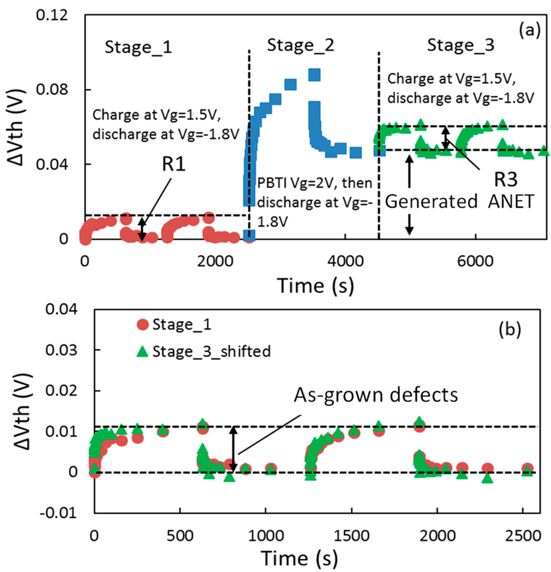
The experience of modeling NBTI shows the importance of separating as-grown defects from the generated ones. The question is whether the electron traps observed in Figure 1342 are as-grown or generated. To answer it, rwesearchers charged and then discharged these electron traps by alternating gate bias polarity in the stage 1 of the test in Figure 143a [48][55]. It can be seen that the charging–discharging was recyclable, indicating that they were as-grown. To further support this, the device was heavily stressed in the stage 2. In the following stage 3, the same gate bias polarity alternation as that in the stage 1 was reapplied. Figure 143b shows that the charging–discharging of electron traps before and after the heavy PBTI stress agrees well, so that they were not affected by the stress, i.e., they are as-grown. After the heavy stress, there are electron traps that cannot be neutralized under Vg = −1.8 V at the end of stage 2. These anti-neutralization electron traps (ANET) did not exist before the heavy stress in the stage 1; thus, they were generated.Figure 1544. (a) Tests for separating as-grown electron traps (AETs) from the as-grown energy-alternating defects (EADs) [39]. (b) When an AET is below Ef, it is charged. (c) The energy levels of the AETs did not change after charging. It was discharged when above the same Ef for its charging. (d) When an EAD is below Ef, it is charged. After charging, the energy level of the EAD is lowered, so that it will not be discharged under the same Ef for its charging in (e).
Figure 1746.
(
a
) AET kinetics under different filling Vgov; (
3.5. As-Grown-Generation (AG) Model of PBTI
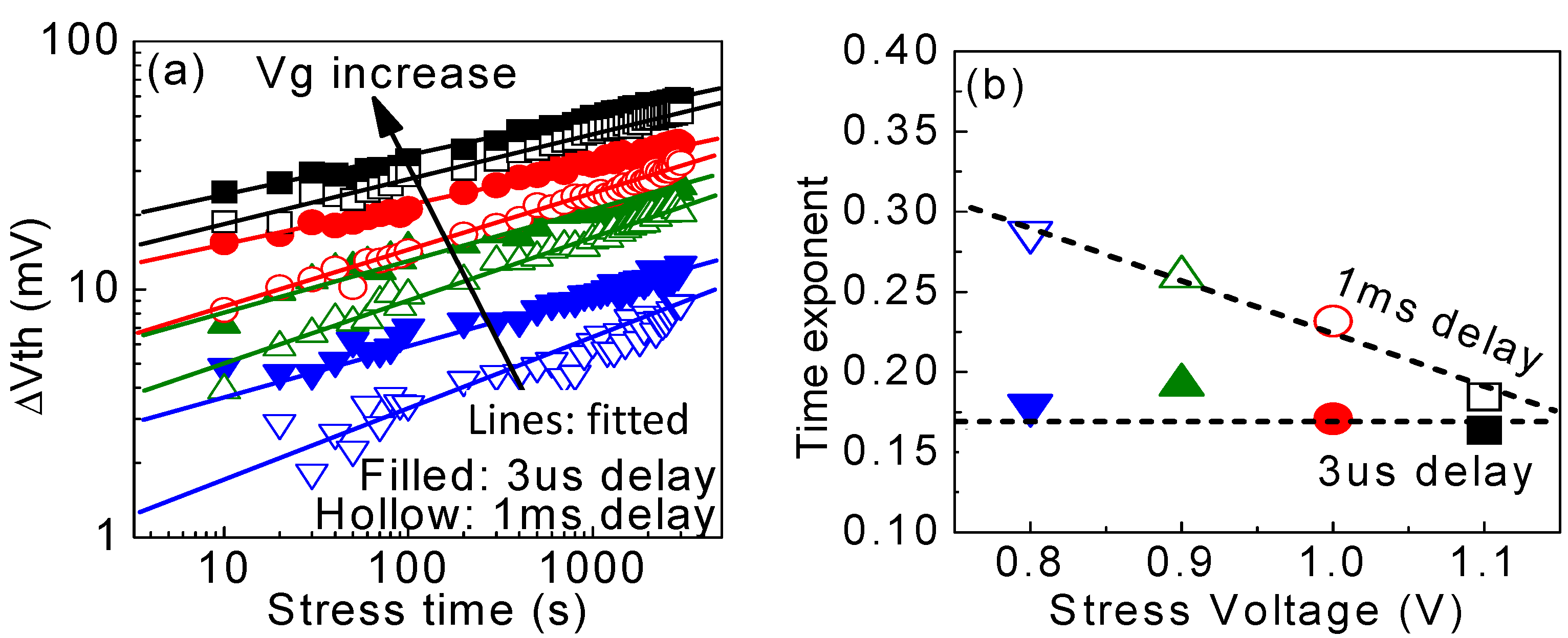
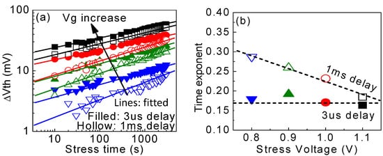
The measured ΔVth during typical PBTI tests consists of both as-grown and generated defects. Although they could fit the power law well in Figure 1847a, the extracted power exponent in Figure 1847b depended on the measured delay [39]. For a delay of 1 ms, typically used in early works, the power exponent also changes with stress bias. When the extracted power law was used to predict PBTI at lower bias, Figure 1948 shows that there were large discrepancies. As a result, the measured ΔVth must not be used to extract the power law directly, and it is essential to separate it into as-grown and generated defects.Figure 1847. (a) Fitting power law with the measured total ΔVth. The lines are fitted, and the symbols are measured data. (b) The extracted power exponent depended on the delay time and stress bias [39].
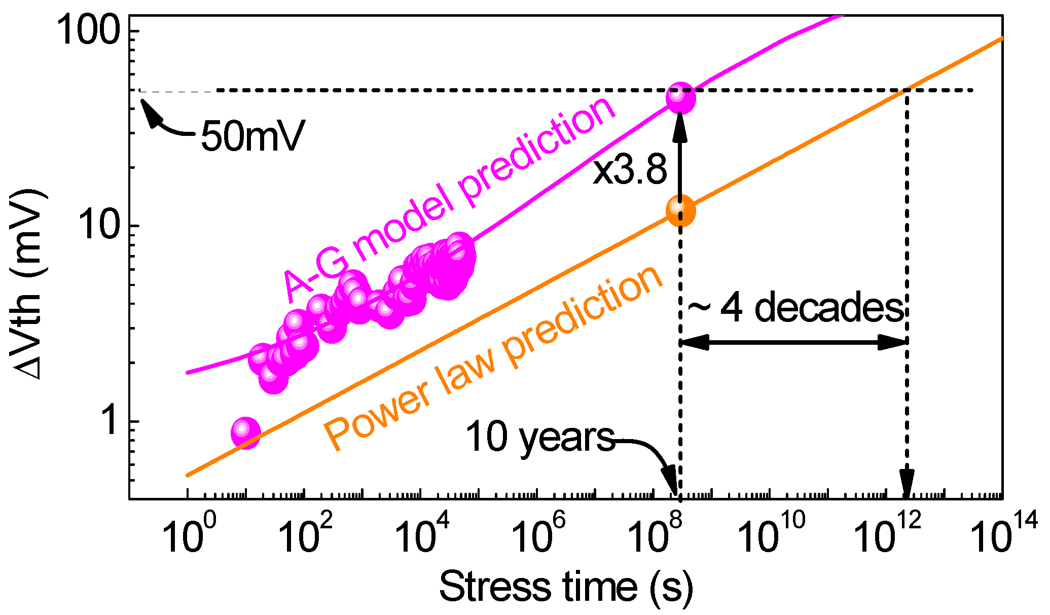
Figure 1948. The AG model extracted from the accelerated PBTI tests can predict the PBTI at low biases, while the power law directly fitted with the same test data overestimates PBTI lifetime by 4 orders of magnitude [39].
Figure 2049. (a) The generated defects measured by the SDR technique were independent of the measurement conditions. (b) The GD kinetics under different stress Vgov. The power exponents were insensitive to Vgov [39].
Table 1. The formula of the as-grown-generation (AG) model for BTI.
| Defects | Formula |
|---|---|
| Saturation level of AHT/AET | ATsat=p1⋅exp(p2⋅Vgov) |
| Filling AHT/AET | AT=ATsat⋅[1−exp(−tchτ)γ] |
| EAD | EAD=g2⋅Vm2gov⋅tn2 |
| GD | GD=g1⋅Vm1gov⋅tn1 |